

Texas Instruments SN74AHCT02DGVR, SN74AHCT02DR, SN74AHCT02N, SN74AHCT02PWLE, SN74AHCT02PWR Datasheet
...
SN54AHCT02, SN74AHCT02
QUADRUPLE 2-INPUT POSITIVE-NOR GATES
SCLS262I – DECEMBER 1995 – REVISED JANUARY 2000
1
POST OFFICE BOX 655303 • DALLAS, TEXAS 75265
D
EPIC
(Enhanced-Performance Implanted
CMOS) Process
D
Inputs Are TTL-Voltage Compatible
D
Latch-Up Performance Exceeds 250 mA Per
JESD 17
D
ESD Protection Exceeds 2000 V Per
MIL-STD-883, Method 3015; Exceeds 200 V
Using Machine Model (C = 200 pF, R = 0)
D
Package Options Include Plastic
Small-Outline (D), Shrink Small-Outline
(DB), Thin Very Small-Outline (DGV), Thin
Shrink Small-Outline (PW), and Ceramic
Flat (W) Packages, Ceramic Chip Carriers
(FK), and Standard Plastic (N) and Ceramic
(J) DIPs
description
These devices contain four independent 2-input
NOR gates that perform the Boolean function
Y = A
S
B or Y = A + B in positive logic.
The SN54AHCT02 is characterized for operation
over the full military temperature range of –55°C
to 125°C. The SN74AHCT02 is characterized for
operation from –40°C to 85°C.
FUNCTION TABLE
(each gate)
INPUTS
OUTPUT
A B
Y
H X L
X HL
L L H
Copyright 2000, Texas Instruments Incorporated
PRODUCTION DATA information is current as of publication date.
Products conform to specifications per the terms of Texas Instruments
standard warranty. Production processing does not necessarily include
testing of all parameters.
Please be aware that an important notice concerning availability, standard warranty, and use in critical applications of
Texas Instruments semiconductor products and disclaimers thereto appears at the end of this data sheet.
EPIC is a trademark of Texas Instruments Incorporated.
1
2
3
4
5
6
7
14
13
12
11
10
9
8
1Y
1A
1B
2Y
2A
2B
GND
V
CC
4Y
4B
4A
3Y
3B
3A
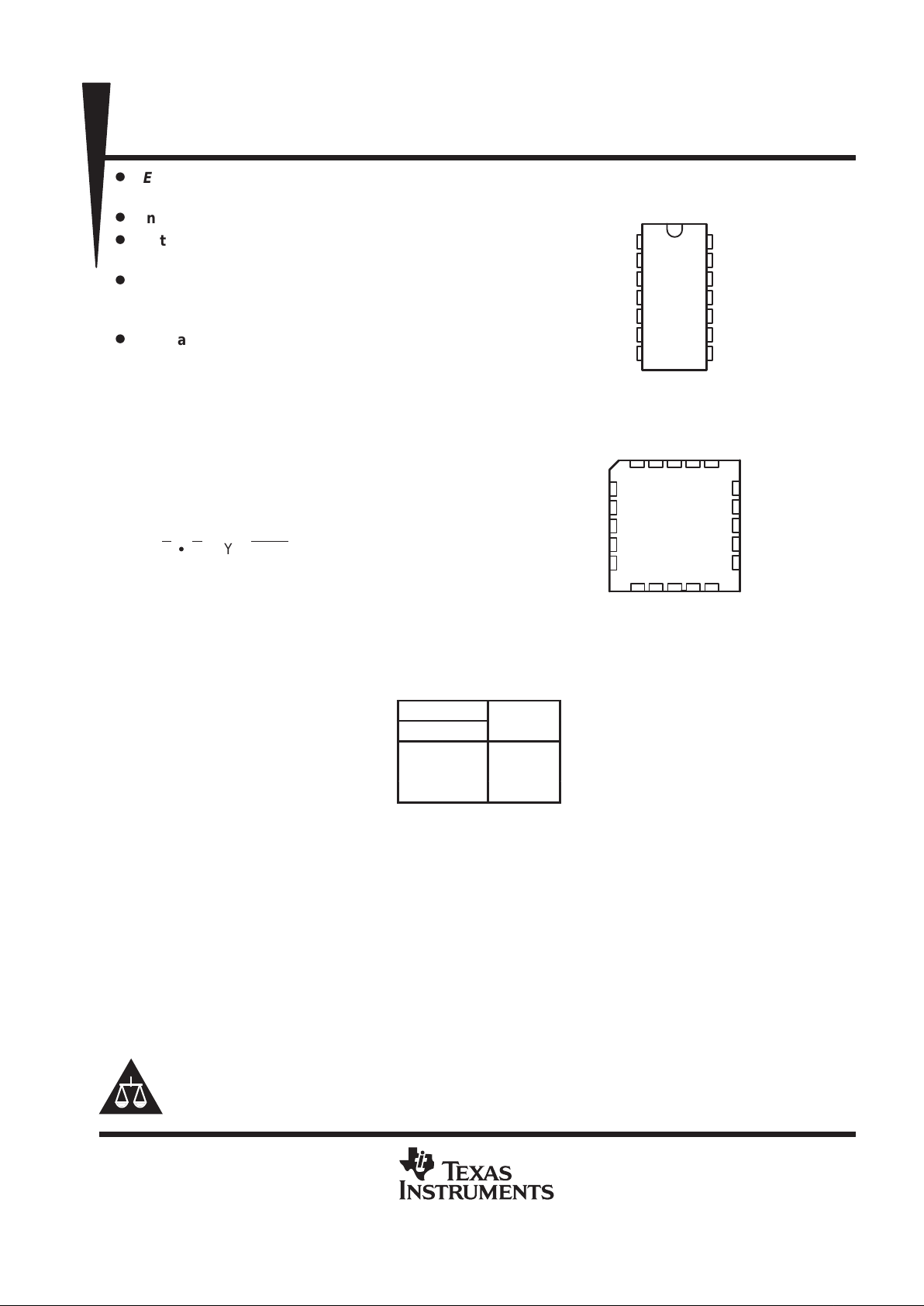
SN54AHCT02 ...J OR W PACKAGE
SN74AHCT02 . . . D, DB, DGV, N, OR PW PACKAGE
(TOP VIEW)
3212019
910111213
4
5
6
7
8
18
17
16
15
14
4B
NC
4A
NC
3Y
1B
NC
2Y
NC
2A
1A1YNC
3A
3B
V
4Y
2B
GND
NC
SN54AHCT02 . . . FK PACKAGE
(TOP VIEW)
CC
NC – No internal connection
On products compliant to MIL-PRF-38535, all parameters are tested
unless otherwise noted. On all other products, production
processing does not necessarily include testing of all parameters.
SN54AHCT02, SN74AHCT02
QUADRUPLE 2-INPUT POSITIVE-NOR GATES
SCLS262I – DECEMBER 1995 – REVISED JANUARY 2000
2
POST OFFICE BOX 655303 • DALLAS, TEXAS 75265
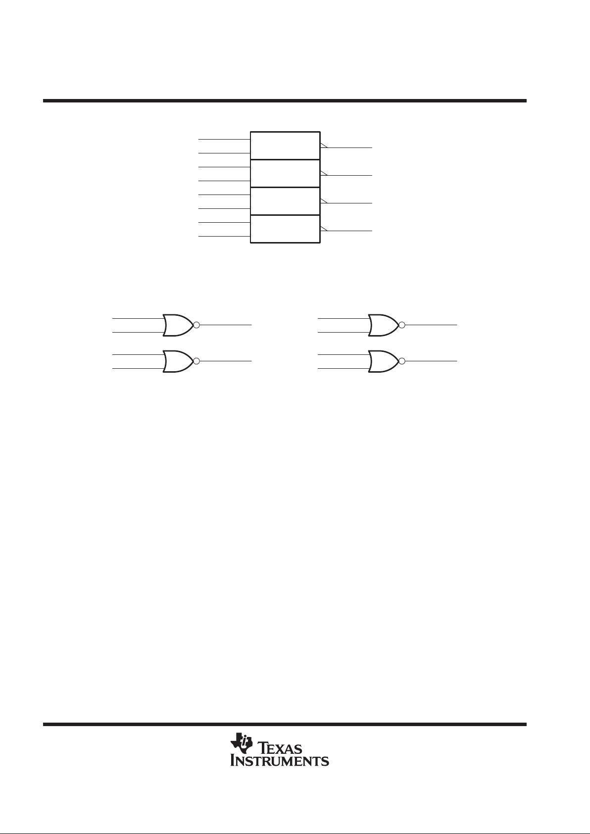
logic symbol
†
†
This symbol is in accordance with ANSI/IEEE Std 91-1984 and IEC Publication 617-12.
Pin numbers shown are for the D, DB, DGV , J, N, PW, and W packages.
2
1A
3
1B
1Y
1
5
2A
6
2B
2Y
4
8
3A
9
3B
3Y
10
11
4A
12
4B
4Y
13
≥ 1
logic diagram (positive logic)
2
1A
3
1B
1Y
1
8
3A
9
3B
3Y
10
5
2A
6
2B
2Y
4
11
4A
12
4B
4Y
13
Pin numbers shown are for the D, DB, DGV, J, N, PW, and W packages.
absolute maximum ratings over operating free-air temperature range (unless otherwise noted)
‡
Supply voltage range, VCC –0.5 V to 7 V. . . . . . . . . . . . . . . . . . . . . . . . . . . . . . . . . . . . . . . . . . . . . . . . . . . . . . . . . .
Input voltage range, V
I
(see Note 1) –0.5 V to 7 V. . . . . . . . . . . . . . . . . . . . . . . . . . . . . . . . . . . . . . . . . . . . . . . . . .
Output voltage range, VO (see Note 1) –0.5 V to VCC + 0.5 V. . . . . . . . . . . . . . . . . . . . . . . . . . . . . . . . . . . . . . . .
Input clamp current, IIK (VI < 0) –20 mA. . . . . . . . . . . . . . . . . . . . . . . . . . . . . . . . . . . . . . . . . . . . . . . . . . . . . . . . . . .
Output clamp current, IOK (VO < 0 or VO > VCC) ±20 mA. . . . . . . . . . . . . . . . . . . . . . . . . . . . . . . . . . . . . . . . . . . .
Continuous output current, IO (VO = 0 to VCC) ±25 mA. . . . . . . . . . . . . . . . . . . . . . . . . . . . . . . . . . . . . . . . . . . . . .
Continuous current through V
CC
or GND ±50 mA. . . . . . . . . . . . . . . . . . . . . . . . . . . . . . . . . . . . . . . . . . . . . . . . . . .
Package thermal impedance, θJA (see Note 2): D package 86°C/W. . . . . . . . . . . . . . . . . . . . . . . . . . . . . . . . . . .
DB package 96°C/W. . . . . . . . . . . . . . . . . . . . . . . . . . . . . . . . .
DGV package 127°C/W. . . . . . . . . . . . . . . . . . . . . . . . . . . . . . .
N package 80°C/W. . . . . . . . . . . . . . . . . . . . . . . . . . . . . . . . . . .
PW package 113°C/W. . . . . . . . . . . . . . . . . . . . . . . . . . . . . . . .
Storage temperature range, T
stg
–65°C to 150°C. . . . . . . . . . . . . . . . . . . . . . . . . . . . . . . . . . . . . . . . . . . . . . . . . . .
‡
Stresses beyond those listed under “absolute maximum ratings” may cause permanent damage to the device. These are stress ratings only, and
functional operation of the device at these or any other conditions beyond those indicated under “recommended operating conditions” is not
implied. Exposure to absolute-maximum-rated conditions for extended periods may affect device reliability.
NOTES: 1. The input and output voltage ratings may be exceeded if the input and output current ratings are observed.
2. The package thermal impedance is calculated in accordance with JESD 51.
 Loading...