

Texas Instruments SN74AHC74D, SN74AHC74DBLE, SN74AHC74DBR, SN74AHC74DGVR, SN74AHC74DR Datasheet
...
SN54AHC74, SN74AHC74
DUAL POSITIVE-EDGE-TRIGGERED D-TYPE FLIP-FLOPS
WITH CLEAR AND PRESET
SCLS255G – DECEMBER 1995 – REVISED JANUARY 20000
D
EPIC
(Enhanced-Performance Implanted
CMOS) Process
D
Operating Range 2-V to 5.5-V V
D
Latch-Up Performance Exceeds 250 mA Per
CC
JESD 17
D
ESD Protection Exceeds 2000 V Per
MIL-STD-883, Method 3015; Exceeds 200 V
Using Machine Model (C = 200 pF, R = 0)
D
Package Options Include Plastic
Small-Outline (D), Shrink Small-Outline
(DB), Thin Very Small-Outline (DGV), Thin
Shrink Small-Outline (PW), and Ceramic
Flat (W) Packages, Ceramic Chip Carriers
(FK), and Standard Plastic (N) and Ceramic
(J) DIPs
description
The ’AHC74 dual positive-edge-triggered devices
are D-type flip-flops.
A low level at the preset (PRE) or clear (CLR)
inputs sets or resets the outputs, regardless of the
levels of the other inputs. When PRE and CLR are
inactive (high), data at the data (D) input meeting
the setup time requirements is transferred to the
outputs on the positive-going edge of the clock
pulse. Clock triggering occurs at a voltage level
and is not directly related to the rise time of the
clock pulse. Following the hold-time interval, data
at the D input can be changed without affecting the
levels at the outputs.
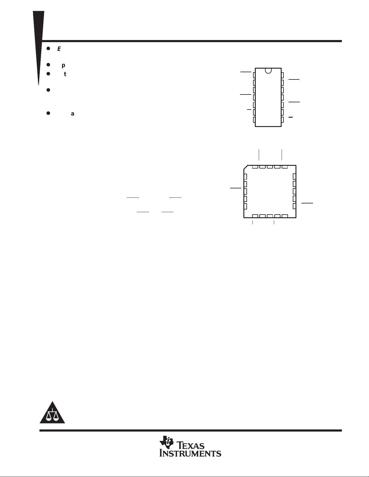
SN54AHC74 ...J OR W PACKAGE
SN74AHC74 . . . D, DB, DGV, N, OR PW PACKAGE
1CLR
1CLK
1PRE
SN54AHC74 . . . FK PACKAGE
1CLK
NC
1PRE
NC
1Q
NC – No internal connection
(TOP VIEW)
1
1D
2
3
4
1Q
5
6
1Q
GND
7
(TOP VIEW)
1D
3212019
4
5
6
7
8
910111213
1Q
1CLR
NC
NC
GND
14
13
12
11
10
9
8
CC
V
2Q
V
CC
2CLR
2D
2CLK
2PRE
2Q
2Q
2CLR
18
17
16
15
14
2Q
2D
NC
2CLK
NC
2PRE
The SN54AHC74 is characterized for operation
over the full military temperature range of –55°C
to 125°C. The SN74AHC74 is characterized for
operation from –40°C to 85°C.
Please be aware that an important notice concerning availability, standard warranty, and use in critical applications of
Texas Instruments semiconductor products and disclaimers thereto appears at the end of this data sheet.
EPIC is a trademark of Texas Instruments Incorporated.
PRODUCTION DATA information is current as of publication date.
Products conform to specifications per the terms of Texas Instruments
standard warranty. Production processing does not necessarily include
testing of all parameters.
Copyright 2000, Texas Instruments Incorporated
On products compliant to MIL-PRF-38535, all parameters are tested
unless otherwise noted. On all other products, production
processing does not necessarily include testing of all parameters.
POST OFFICE BOX 655303 • DALLAS, TEXAS 75265
1
SN54AHC74, SN74AHC74
DUAL POSITIVE-EDGE-TRIGGERED D-TYPE FLIP-FLOPS
WITH CLEAR AND PRESET
SCLS255G – DECEMBER 1995 – REVISED JANUARY 20000
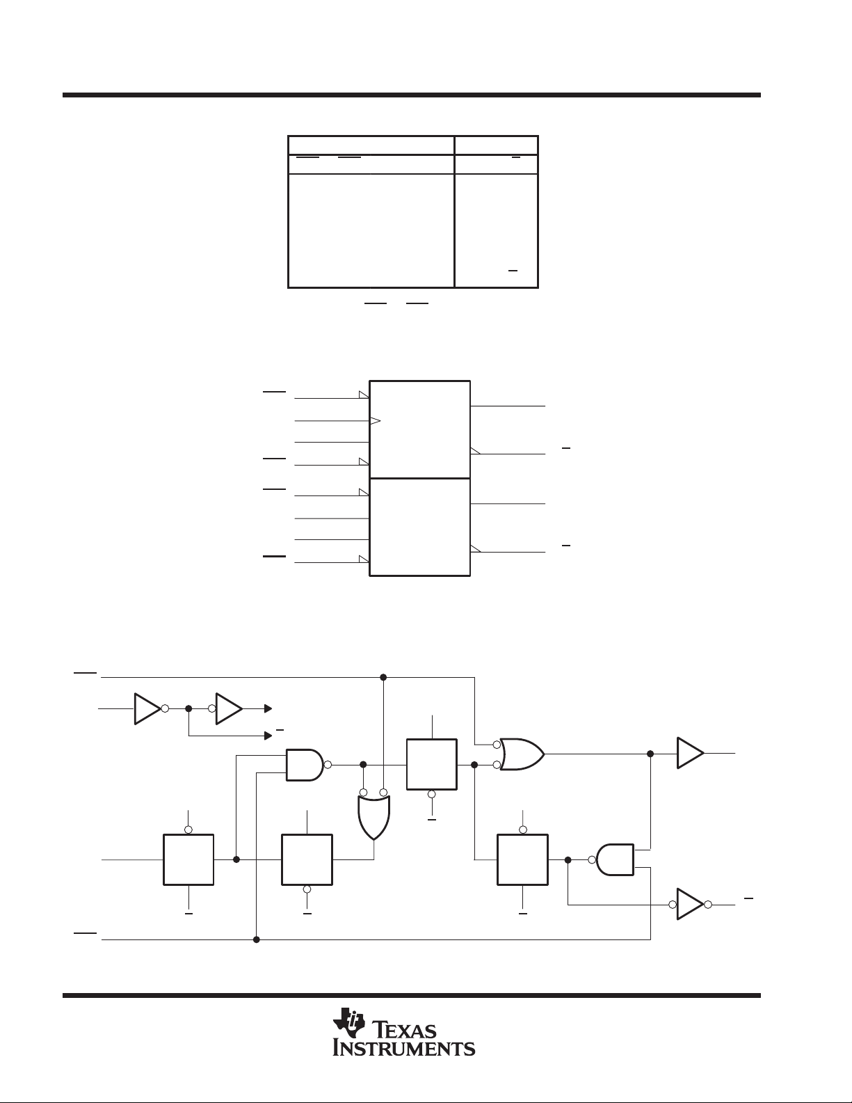
FUNCTION TABLE
(each flip-flop)
INPUTS
PRE CLR CLK D Q Q
L H X X H L
H LXXLH
L LXXH†H
H H ↑ HHL
H H ↑ LLH
H H L X Q
†
This configuration is nonstable; that is, it does not
persist when PRE
(high) level.
or CLR returns to its inactive
OUTPUTS
0
†
Q
0
logic symbol
‡
This symbol is in accordance with ANSI/IEEE Std 91-1984 and IEC Publication 617-12.
Pin numbers shown are for the D, DB, DGV, J, N, PW, and W packages.
‡
1PRE
1CLK
1D
1CLR
2PRE
2CLK
2D
2CLR
4
3
2
1
10
11
12
13
S
C1
1D
R
logic diagram, each flip-flop (positive logic)
PRE
CLK
C
C
C
TG
5
1Q
6
1Q
9
2Q
8
2Q
Q
2
CLR
C
D
TG
C
C
C
TG
C
POST OFFICE BOX 655303 • DALLAS, TEXAS 75265
C
TG
Q
C
UNIT
mA
mA
∆t/∆vInput transition rise or fall rate
ns/V
SN54AHC74, SN74AHC74
DUAL POSITIVE-EDGE-TRIGGERED D-TYPE FLIP-FLOPS
WITH CLEAR AND PRESET
SCLS255G – DECEMBER 1995 – REVISED JANUARY 20000
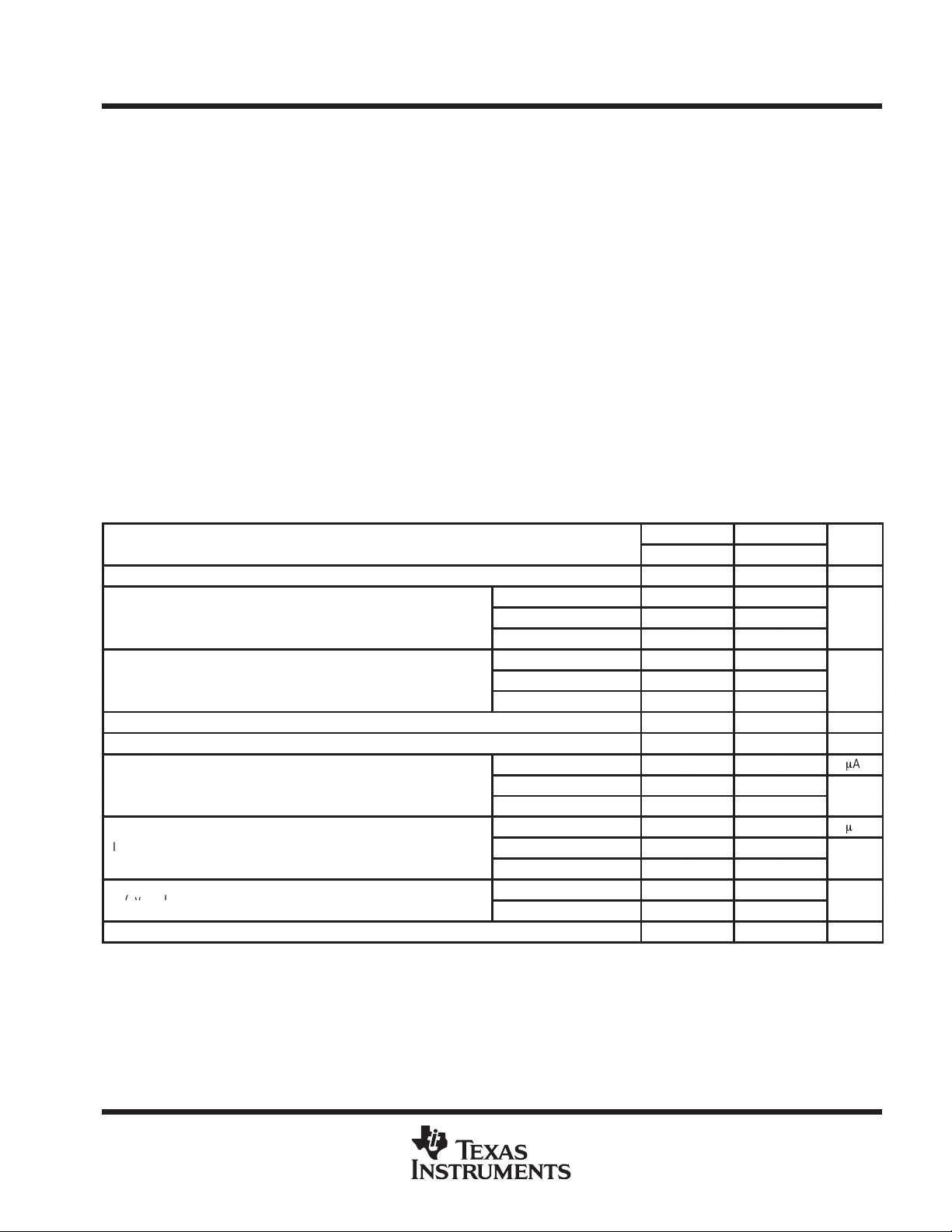
absolute maximum ratings over operating free-air temperature range (unless otherwise noted)
†
Supply voltage range, VCC –0.5 V to 7 V. . . . . . . . . . . . . . . . . . . . . . . . . . . . . . . . . . . . . . . . . . . . . . . . . . . . . . . . . .
Input voltage range, VI (see Note 1) –0.5 V to 7 V. . . . . . . . . . . . . . . . . . . . . . . . . . . . . . . . . . . . . . . . . . . . . . . . . .
Output voltage range, V
Input clamp current, I
Output clamp current, I
(see Note 1) –0.5 V to V
O
(V
IK
I
OK
Continuous output current, I
< 0) –20 mA. . . . . . . . . . . . . . . . . . . . . . . . . . . . . . . . . . . . . . . . . . . . . . . . . . . . . . . . . . .
(V
< 0 or VO > VCC) ±20 mA. . . . . . . . . . . . . . . . . . . . . . . . . . . . . . . . . . . . . . . . . . . .
O
(V
= 0 to VCC) ±25 mA. . . . . . . . . . . . . . . . . . . . . . . . . . . . . . . . . . . . . . . . . . . . . .
O
O
CC
+ 0.5 V. . . . . . . . . . . . . . . . . . . . . . . . . . . . . . . . . . . . . . . .
Continuous current through VCC or GND ±50 mA. . . . . . . . . . . . . . . . . . . . . . . . . . . . . . . . . . . . . . . . . . . . . . . . . . .
Package thermal impedance, θ
(see Note 2): D package 86°C/W. . . . . . . . . . . . . . . . . . . . . . . . . . . . . . . . . . .
JA
DB package 96°C/W. . . . . . . . . . . . . . . . . . . . . . . . . . . . . . . . .
DGV package 127°C/W. . . . . . . . . . . . . . . . . . . . . . . . . . . . . . .
N package 80°C/W. . . . . . . . . . . . . . . . . . . . . . . . . . . . . . . . . . .
PW package 113°C/W. . . . . . . . . . . . . . . . . . . . . . . . . . . . . . . .
Storage temperature range, T
†
Stresses beyond those listed under “absolute maximum ratings” may cause permanent damage to the device. These are stress ratings only, and
functional operation of the device at these or any other conditions beyond those indicated under “recommended operating conditions” is not
implied. Exposure to absolute-maximum-rated conditions for extended periods may affect device reliability.
NOTES: 1. The input and output voltage ratings may be exceeded if the input and output current ratings are observed.
2. The package thermal impedance is calculated in accordance with JESD 51.
–65°C to 150°C. . . . . . . . . . . . . . . . . . . . . . . . . . . . . . . . . . . . . . . . . . . . . . . . . . .
stg
recommended operating conditions (see Note 3)
SN54AHC74 SN74AHC74
MIN MAX MIN MAX
V
V
V
V
V
I
OH
I
OL
T
NOTE 3: All unused inputs of the device must be held at VCC or GND to ensure proper device operation. Refer to the TI application report,
Supply voltage 2 5.5 2 5.5 V
CC
VCC = 2 V 1.5 1.5
High-level input voltage
IH
Low-level input voltage
IL
Input voltage 0 5.5 0 5.5 V
I
Output voltage 0 V
O
High-level output current
Low-level output current
p
Operating free-air temperature –55 125 –40 85 °C
A
Implications of Slow or Floating CMOS Inputs
, literature number SCBA004.
VCC = 3 V
VCC = 5.5 V 3.85 3.85
VCC = 2 V 0.5 0.5
VCC = 3 V
VCC = 5.5 V 1.65 1.65
VCC = 2 V –50 –50
VCC = 3.3 V ± 0.3 V
VCC = 5 V ± 0.5 V –8 –8
VCC = 2 V 50 50
VCC = 3.3 V ± 0.3 V
VCC = 5 V ± 0.5 V 8 8
VCC = 3.3 V ± 0.3 V 100 100
VCC = 5 V ± 0.5 V 20 20
2.1 2.1
0.9 0.9
CC
–4 –4
4 4
0 V
CC
V
V
V
m
A
m
A
POST OFFICE BOX 655303 • DALLAS, TEXAS 75265
3
 Loading...