

Texas Instruments SN74AHC373DBLE, SN74AHC373DBR, SN74AHC373DGVR, SN74AHC373DW, SN74AHC373DWR Datasheet
...
SN54AHC373, SN74AHC373
OCTAL TRANSPARENT D-TYPE LATCHES
WITH 3-STATE OUTPUTS
SCLS235G – OCTOBER 1995 – REVISED JANUARY 2000
D
EPIC
(Enhanced-Performance Implanted
CMOS) Process
D
Operating Range 2-V to 5.5-V V
D
Latch-Up Performance Exceeds 250 mA Per
CC
JESD 17
D
ESD Protection Exceeds 2000 V Per
MIL-STD-883, Method 3015; Exceeds 200 V
Using Machine Model (C = 200 pF, R = 0)
D
Package Options Include Plastic
Small-Outline (DW), Shrink Small-Outline
(DB), Thin Very Small-Outline (DGV), Thin
Shrink Small-Outline (PW), and Ceramic
Flat (W) Packages, Ceramic Chip Carriers
(FK), and Standard Plastic (N) and Ceramic
(J) DIPs
description
The ’AHC373 devices are octal transparent
D-type latches designed for 2-V to 5.5-V V
operation.
When the latch-enable (LE) input is high, the
Q outputs follow the data (D) inputs. When LE is
low, the Q outputs are latched at the logic levels
of the D inputs.
CC
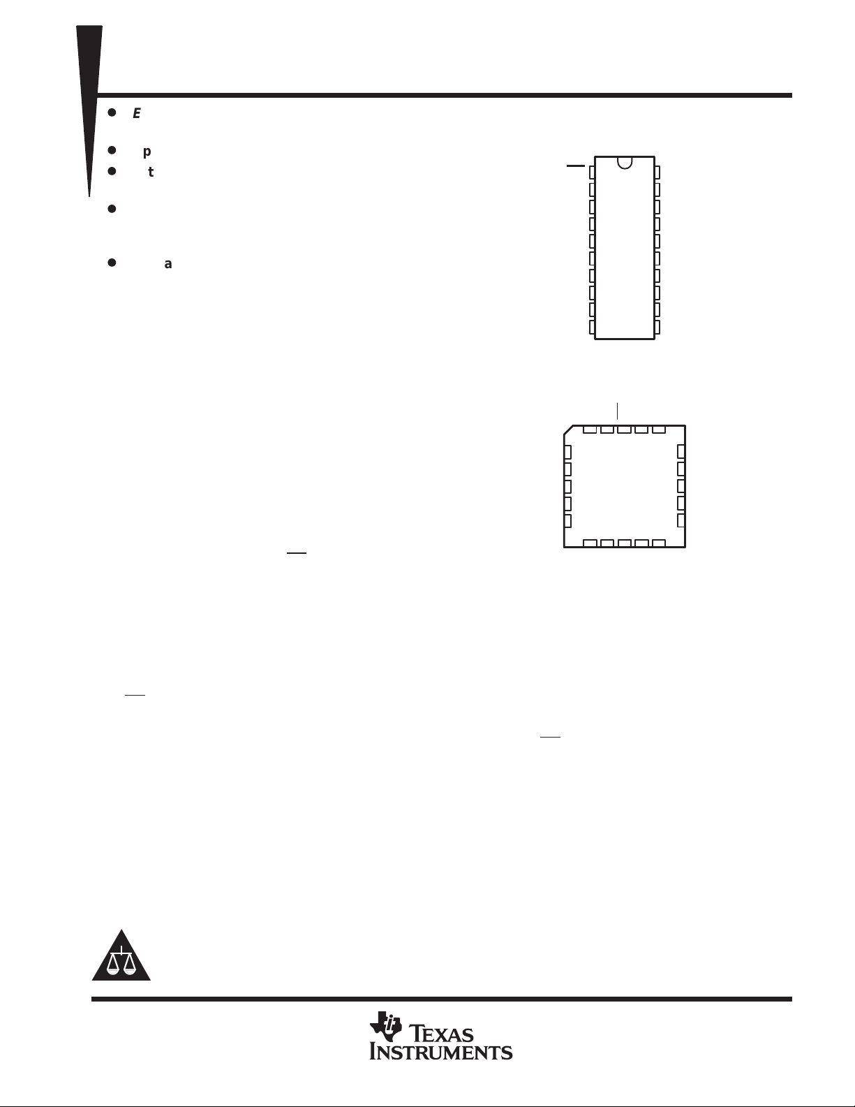
SN74AHC373 . . . DB, DGV, DW, N, OR PW PACKAGE
SN54AHC373 ...J OR W PACKAGE
(TOP VIEW)
OE
1
1Q
2
1D
3
2D
4
5
2Q
6
3Q
7
3D
8
4D
9
4Q
10
GND
SN54AHC373 . . . FK PACKAGE
2D
2Q
3Q
3D
4D
(TOP VIEW)
1D1QOE
3 2 1 20 19
4
5
6
7
8
9 10 11 12 13
20
19
18
17
16
15
14
13
12
11
V
CC
8Q
8D
7D
7Q
6Q
6D
5D
5Q
LE
CC
V
8Q
8D
18
7D
17
7Q
16
6Q
15
14
6D
A buffered output-enable (OE
to place the eight outputs in either a normal logic
) input can be used
4Q
GND
LE
5Q
5D
state (high or low) or the high-impedance state. In
the high-impedance state, the outputs neither
load nor drive the bus lines significantly. The
high-impedance state and increased drive provide
the capability to drive bus lines without interface
or pullup components.
OE
does not affect the internal operations of the latches. Old data can be retained or new data can be entered
while the outputs are in the high-impedance state.
T o ensure the high-impedance state during power up or power down, OE should be tied to V
through a pullup
CC
resistor; the minimum value of the resistor is determined by the current-sinking capability of the driver.
The SN54AHC373 is characterized for operation over the full military temperature range of –55°C to 125°C.
The SN74AHC373 is characterized for operation from –40°C to 85°C.
Please be aware that an important notice concerning availability, standard warranty, and use in critical applications of
Texas Instruments semiconductor products and disclaimers thereto appears at the end of this data sheet.
EPIC is a trademark of Texas Instruments Incorporated.
PRODUCTION DATA information is current as of publication date.
Products conform to specifications per the terms of Texas Instruments
standard warranty. Production processing does not necessarily include
testing of all parameters.
POST OFFICE BOX 655303 • DALLAS, TEXAS 75265
Copyright 2000, Texas Instruments Incorporated
On products compliant to MIL-PRF-38535, all parameters are tested
unless otherwise noted. On all other products, production
processing does not necessarily include testing of all parameters.
1
SN54AHC373, SN74AHC373
OCTAL TRANSPARENT D-TYPE LATCHES
WITH 3-STATE OUTPUTS
SCLS235G – OCTOBER 1995 – REVISED JANUARY 2000
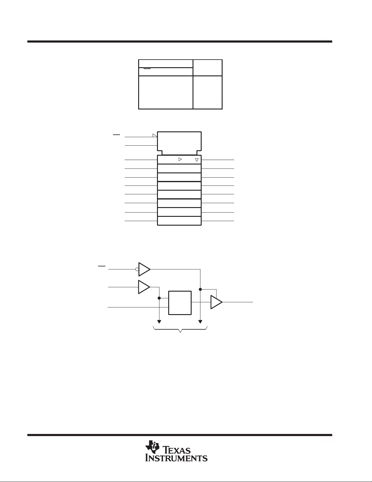
FUNCTION TABLE
INPUTS
OE LE D
L H H H
L HL L
L LX Q
H X X Z
(each latch)
OUTPUT
Q
0
logic symbol
†
This symbol is in accordance with ANSI/IEEE Std 91-1984 and IEC Publication 617-12.
†
OE
LE
1D
2D
3D
4D
5D
6D
7D
8D
1
11
3
4
7
8
13
14
17
18
EN
C1
1D
logic diagram (positive logic)
1
OE
11
LE
12
15
16
19
2
1Q
5
2Q
6
3Q
9
4Q
5Q
6Q
7Q
8Q
3
1D
To Seven Other Channels
2
POST OFFICE BOX 655303 • DALLAS, TEXAS 75265
C1
1D
2
1Q
UNIT
mA
mA
∆t/∆vInput transition rise or fall rate
ns/V
SN54AHC373, SN74AHC373
OCTAL TRANSPARENT D-TYPE LATCHES
WITH 3-STATE OUTPUTS
SCLS235G – OCTOBER 1995 – REVISED JANUARY 2000
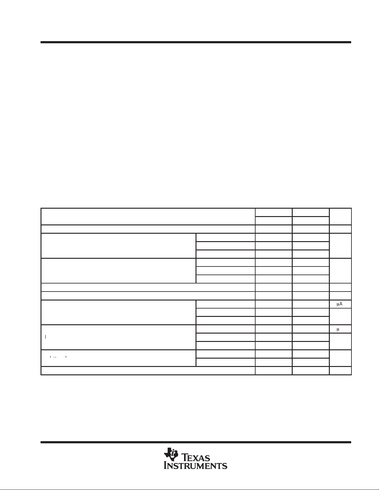
absolute maximum ratings over operating free-air temperature range (unless otherwise noted)
†
Supply voltage range, VCC –0.5 V to 7 V. . . . . . . . . . . . . . . . . . . . . . . . . . . . . . . . . . . . . . . . . . . . . . . . . . . . . . . . . .
Input voltage range, VI (see Note 1) –0.5 V to 7 V. . . . . . . . . . . . . . . . . . . . . . . . . . . . . . . . . . . . . . . . . . . . . . . . . .
Output voltage range, V
Input clamp current, I
Output clamp current, I
(see Note 1) –0.5 V to V
O
(V
IK
I
OK
Continuous output current, I
< 0) –20 mA. . . . . . . . . . . . . . . . . . . . . . . . . . . . . . . . . . . . . . . . . . . . . . . . . . . . . . . . . . .
(V
< 0 or VO > VCC) ±20 mA. . . . . . . . . . . . . . . . . . . . . . . . . . . . . . . . . . . . . . . . . . . .
O
(V
= 0 to VCC) ±25 mA. . . . . . . . . . . . . . . . . . . . . . . . . . . . . . . . . . . . . . . . . . . . . .
O
O
CC
+ 0.5 V. . . . . . . . . . . . . . . . . . . . . . . . . . . . . . . . . . . . . . . .
Continuous current through VCC or GND ±75 mA. . . . . . . . . . . . . . . . . . . . . . . . . . . . . . . . . . . . . . . . . . . . . . . . . . .
Package thermal impedance, θ
(see Note 2): DB package 70°C/W. . . . . . . . . . . . . . . . . . . . . . . . . . . . . . . . .
JA
DGV package 92°C/W. . . . . . . . . . . . . . . . . . . . . . . . . . . . . . . .
DW package 58°C/W. . . . . . . . . . . . . . . . . . . . . . . . . . . . . . . . .
N package 69°C/W. . . . . . . . . . . . . . . . . . . . . . . . . . . . . . . . . . .
PW package 83°C/W. . . . . . . . . . . . . . . . . . . . . . . . . . . . . . . . .
Storage temperature range, T
†
Stresses beyond those listed under “absolute maximum ratings” may cause permanent damage to the device. These are stress ratings only, and
functional operation of the device at these or any other conditions beyond those indicated under “recommended operating conditions” is not
implied. Exposure to absolute-maximum-rated conditions for extended periods may affect device reliability.
NOTES: 1. The input and output voltage ratings may be exceeded if the input and output current ratings are observed.
2. The package thermal impedance is calculated in accordance with JESD 51.
–65°C to 150°C. . . . . . . . . . . . . . . . . . . . . . . . . . . . . . . . . . . . . . . . . . . . . . . . . . .
stg
recommended operating conditions (see Note 3)
SN54AHC373 SN74AHC373
MIN MAX MIN MAX
V
V
V
V
V
I
OH
I
OL
T
NOTE 3: All unused inputs of the device must be held at VCC or GND to ensure proper device operation. Refer to the TI application report,
Supply voltage 2 5.5 2 5.5 V
CC
VCC = 2 V 1.5 1.5
High-level input voltage
IH
Low-level input voltage
IL
Input voltage 0 5.5 0 5.5 V
I
Output voltage 0 V
O
High-level output current
Low-level output current
p
Operating free-air temperature –55 125 –40 85 °C
A
Implications of Slow or Floating CMOS Inputs
, literature number SCBA004.
VCC = 3 V
VCC = 5.5 V 3.85 3.85
VCC = 2 V 0.5 0.5
VCC = 3 V
VCC = 5.5 V 1.65 1.65
VCC = 2 V –50 –50
VCC = 3.3 V ± 0.3 V
VCC = 5 V ± 0.5 V –8 –8
VCC = 2 V 50 50
VCC = 3.3 V ± 0.3 V
VCC = 5 V ± 0.5 V 8 8
VCC = 3.3 V ± 0.3 V 100 100
VCC = 5 V ± 0.5 V 20 20
2.1 2.1
0.9 0.9
CC
–4 –4
4 4
0 V
CC
V
V
V
m
A
m
A
POST OFFICE BOX 655303 • DALLAS, TEXAS 75265
3
 Loading...