

Texas Instruments SN74AHC240DBLE, SN74AHC240DBR, SN74AHC240DGVR, SN74AHC240DW, SN74AHC240DWR Datasheet
...
SN54AHC240, SN74AHC240
OCTAL BUFFERS/DRIVERS
WITH 3-STATE OUTPUTS
SCLS251F – OCTOBER 1995 – REVISED JANUARY 2000
D
EPIC
(Enhanced-Performance Implanted
CMOS) Process
D
Operating Range 2-V to 5.5-V V
D
Latch-Up Performance Exceeds 250 mA
CC
Per JESD 17
D
Package Options Include Plastic
Small-Outline (DW), Shrink Small-Outline
(DB), Thin Very Small-Outline (DGV), Thin
Shrink Small-Outline (PW), and Ceramic
Flat (W) Packages, Ceramic Chip Carriers
(FK), and Standard Plastic (N) and Ceramic
(J) DIPs
description
These octal buffers/drivers are designed
specifically to improve the performance and
density of 3-state memory-address drivers, clock
drivers, and bus-oriented receivers and
transmitters.
The ’AHC240 devices are organized as two 4-bit
buffers/line drivers with separate output-enable
(OE
) inputs. When OE is low, the device passes
data from the A inputs to the Y outputs. When OE
is high, the outputs are in the high-impedance
state.
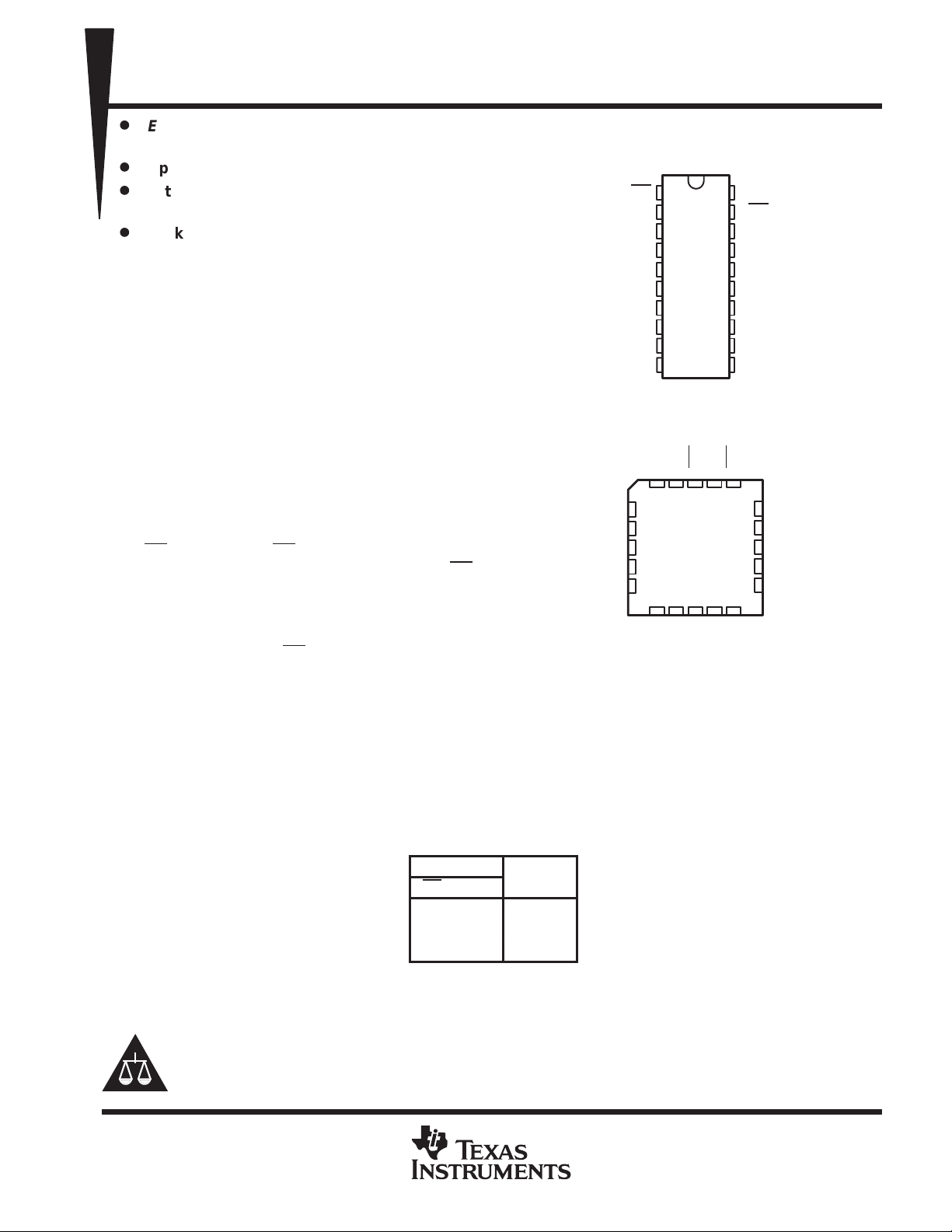
SN74AHC240 . . . DB, DGV, DW, N, OR PW PACKAGE
SN54AHC240 ...J OR W PACKAGE
(TOP VIEW)
1OE
1
1A1
2
2Y4
3
1A2
4
2Y3
5
1A3
6
2Y2
7
1A4
8
9
2Y1
GND
SN54AHC240 . . . FK PACKAGE
1A2
2Y3
1A3
2Y2
1A4
10
(TOP VIEW)
2Y4
1A1
3212019
4
5
6
7
8
910111213
20
19
18
17
16
15
14
13
12
11
1OE
V
CC
V
CC
2OE
1Y1
2A4
1Y2
2A3
1Y3
2A2
1Y4
2A1
18
17
16
15
14
1Y1
2A4
1Y2
2A3
1Y3
T o ensure the high-impedance state during power
up or power down, OE should be tied to V
CC
2Y1
GND
2A1
1Y4
2A2 2OE
through a pullup resistor; the minimum value of
the resistor is determined by the current-sinking
capability of the driver.
The SN54AHC240 is characterized for operation
over the full military temperature range of –55°C
to 125°C. The SN74AHC240 is characterized for
operation from –40°C to 85°C.
FUNCTION TABLE
(each 4-bit buffer/driver)
INPUTS
OE A
L H L
L LH
H X Z
Please be aware that an important notice concerning availability, standard warranty, and use in critical applications of
Texas Instruments semiconductor products and disclaimers thereto appears at the end of this data sheet.
OUTPUT
Y
EPIC is a trademark of Texas Instruments Incorporated.
PRODUCTION DATA information is current as of publication date.
Products conform to specifications per the terms of Texas Instruments
standard warranty. Production processing does not necessarily include
testing of all parameters.
POST OFFICE BOX 655303 • DALLAS, TEXAS 75265
Copyright 2000, Texas Instruments Incorporated
On products compliant to MIL-PRF-38535, all parameters are tested
unless otherwise noted. On all other products, production
processing does not necessarily include testing of all parameters.
1
SN54AHC240, SN74AHC240
OCTAL BUFFERS/DRIVERS
WITH 3-STATE OUTPUTS
SCLS251F – OCTOBER 1995 – REVISED JANUARY 2000
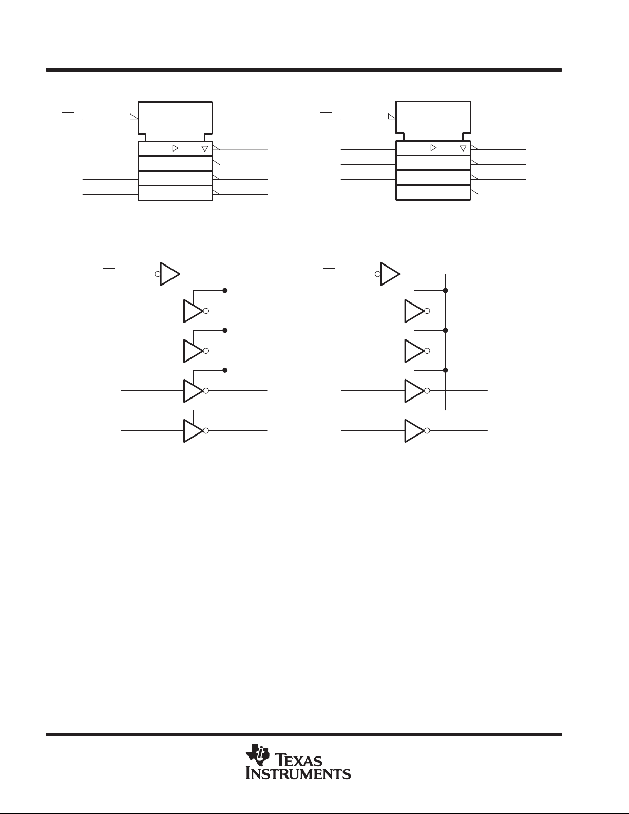
logic symbol
1OE
1A1
1A2
1A3
1A4
†
This symbol is in accordance with ANSI/IEEE Std 91-1984 and IEC Publication 617-12.
†
1
2
4
6
8
EN
18
16
14
12
1Y1
1Y2
1Y3
1Y4
2OE
2A1
2A2
2A3
2A4
logic diagram (positive logic)
1
1OE
218
1A1
416
1A2
1Y1
1Y2
2OE
2A1
2A2
19
11
13
15
17
19
11 9
13 7
EN
2Y1
2Y2
9
2Y1
7
2Y2
5
2Y3
3
2Y4
614
1A3
812
1A4
1Y3
1Y4
15 5
2A3
17 3
2A4
2Y3
2Y4
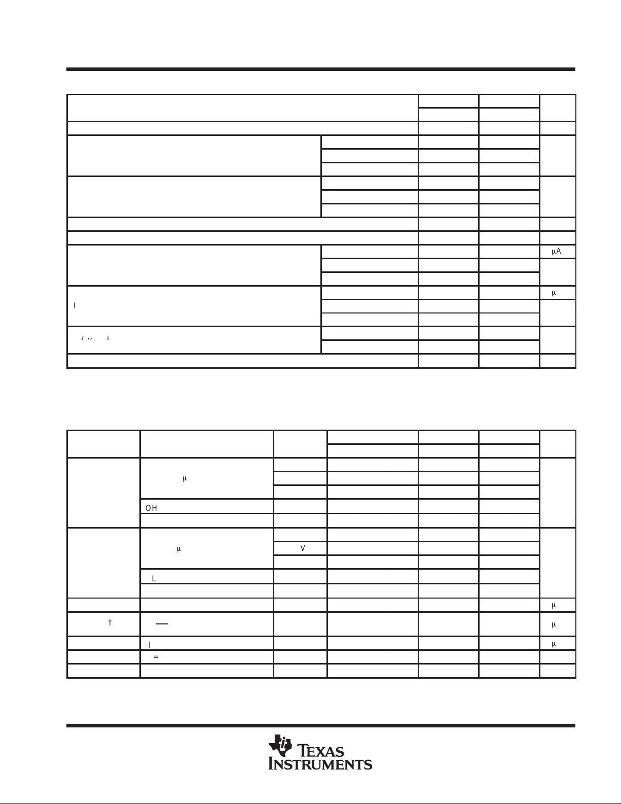
absolute maximum ratings over operating free-air temperature range (unless otherwise noted)
Supply voltage range, VCC –0.5 V to 7 V. . . . . . . . . . . . . . . . . . . . . . . . . . . . . . . . . . . . . . . . . . . . . . . . . . . . . . . . . .
Input voltage range, VI (see Note 1) –0.5 V to 7 V. . . . . . . . . . . . . . . . . . . . . . . . . . . . . . . . . . . . . . . . . . . . . . . . . .
Output voltage range, VO (see Note 1) –0.5 V to V
Input clamp current, I
Output clamp current, I
Continuous output current, I
(V
< 0) –20 mA. . . . . . . . . . . . . . . . . . . . . . . . . . . . . . . . . . . . . . . . . . . . . . . . . . . . . . . . . . .
IK
I
(V
OK
< 0 or VO > VCC) ±20 mA. . . . . . . . . . . . . . . . . . . . . . . . . . . . . . . . . . . . . . . . . . . .
O
(V
= 0 to VCC) ±25 mA. . . . . . . . . . . . . . . . . . . . . . . . . . . . . . . . . . . . . . . . . . . . . .
O
O
Continuous current through VCC or GND ±75 mA. . . . . . . . . . . . . . . . . . . . . . . . . . . . . . . . . . . . . . . . . . . . . . . . . . .
Package thermal impedance, θJA (see Note 2): DB package 70°C/W. . . . . . . . . . . . . . . . . . . . . . . . . . . . . . . . .
DGV package 92°C/W. . . . . . . . . . . . . . . . . . . . . . . . . . . . . . . .
DW package 58°C/W. . . . . . . . . . . . . . . . . . . . . . . . . . . . . . . . .
N package 69°C/W. . . . . . . . . . . . . . . . . . . . . . . . . . . . . . . . . . .
PW package 83°C/W. . . . . . . . . . . . . . . . . . . . . . . . . . . . . . . . .
Storage temperature range, T
‡
Stresses beyond those listed under “absolute maximum ratings” may cause permanent damage to the device. These are stress ratings only, and
functional operation of the device at these or any other conditions beyond those indicated under “recommended operating conditions” is not
implied. Exposure to absolute-maximum-rated conditions for extended periods may affect device reliability.
NOTES: 1. The input and output voltage ratings may be exceeded if the input and output current ratings are observed.
2. The package thermal impedance is calculated in accordance with JESD 51.
–65°C to 150°C. . . . . . . . . . . . . . . . . . . . . . . . . . . . . . . . . . . . . . . . . . . . . . . . . . .
stg
CC
+ 0.5 V. . . . . . . . . . . . . . . . . . . . . . . . . . . . . . . . . . . . . . . .
‡
2
POST OFFICE BOX 655303 • DALLAS, TEXAS 75265
UNIT
mA
mA
∆t/∆vInput transition rise or fall rate
ns/V
PARAMETER
TEST CONDITIONS
V
UNIT
OH
OL
SN54AHC240, SN74AHC240
OCTAL BUFFERS/DRIVERS
WITH 3-STATE OUTPUTS
SCLS251F – OCTOBER 1995 – REVISED JANUARY 2000
recommended operating conditions (see Note 3)
SN54AHC240 SN74AHC240
MIN MAX MIN MAX
V
V
V
V
V
I
OH
I
OL
T
NOTE 3: All unused inputs of the device must be held at VCC or GND to ensure proper device operation. Refer to the TI application report,
Supply voltage 2 5.5 2 5.5 V
CC
VCC = 2 V 1.5 1.5
High-level input voltage
IH
Low-level input voltage
IL
Input voltage 0 5.5 0 5.5 V
I
Output voltage 0 V
O
High-level output current
Low-level output current
p
Operating free-air temperature –55 125 –40 85 °C
A
Implications of Slow or Floating CMOS Inputs
, literature number SCBA004.
VCC = 3 V
VCC = 5.5 V 3.85 3.85
VCC = 2 V 0.5 0.5
VCC = 3 V
VCC = 5.5 V 1.65 1.65
VCC = 2 V –50 –50
VCC = 3.3 V ± 0.3 V
VCC = 5 V ± 0.5 V –8 –8
VCC = 2 V 50 50
VCC = 3.3 V ± 0.3 V
VCC = 5 V ± 0.5 V 8 8
VCC = 3.3 V ± 0.3 V 100 100
VCC = 5 V ± 0.5 V 20 20
2.1 2.1
0.9 0.9
CC
–4 –4
4 4
0 V
CC
V
V
V
m
A
m
A
electrical characteristics over recommended operating free-air temperature range (unless
otherwise noted)
CC
2 V 1.9 2 1.9 1.9
IOH = –50 mA
V
OH
IOH = –4 mA
IOH = –8 mA
IOL = 50 mA
V
OL
IOL = 4 mA
IOL = 8 mA
I
I
†
I
OZ
I
CC
C
i
C
o
* On products compliant to MIL-PRF-38535, this parameter is not production tested at VCC = 0 V.
†
The parameter IOZ includes the input leakage current.
VI = VCC or GND 0 V to 5.5 V ±0.1 ±1* ±1
VO = VCC or GND,
VI (OE
) = VIL or V
VI = VCC or GND, IO = 0 5.5 V 4 40 40
VI = VCC or GND 5 V 2.5 10 10 pF
VO = VCC or GND 5 V 3.5 pF
IH
3 V 2.9 3 2.9 2.9
4.5 V 4.4 4.5 4.4 4.4
3 V 2.58 2.48 2.48
4.5 V 3.94 3.8 3.8
2 V 0.1 0.1 0.1
3 V 0.1 0.1 0.1
4.5 V 0.1 0.1 0.1
3 V 0.36 0.5 0.44
4.5 V 0.36 0.5 0.44
5.5 V ±0.25 ±2.5 ±2.5
TA = 25°C SN54AHC240 SN74AHC240
MIN TYP MAX MIN MAX MIN MAX
V
V
m
A
m
A
m
A
POST OFFICE BOX 655303 • DALLAS, TEXAS 75265
3
 Loading...