

Texas Instruments SN74AHC138, SN74AHC138D, SN74AHC138DBLE, SN74AHC138DBR, SN74AHC138DGVR Datasheet
...
SN54AHC138, SN74AHC138
3-LINE TO 8-LINE DECODERS/DEMULTIPLEXERS
SCLS258I – DECEMBER 1995 – REVISED JANUARY 2000
D
EPIC
(Enhanced-Performance Implanted
CMOS) Process
D
Operating Range 2-V to 5.5-V V
D
Designed Specifically for High-Speed
CC
Memory Decoders and Data-Transmission
Systems
D
Incorporate Three Enable Inputs to Simplify
Cascading and/or Data Reception
D
Latch-Up Performance Exceeds 250 mA Per
JESD 17
D
ESD Protection Exceeds 2000 V Per
MIL-STD-833, Method 3015; Exceeds 200 V
Using Machine Model (C = 200 pF, R = 0)
D
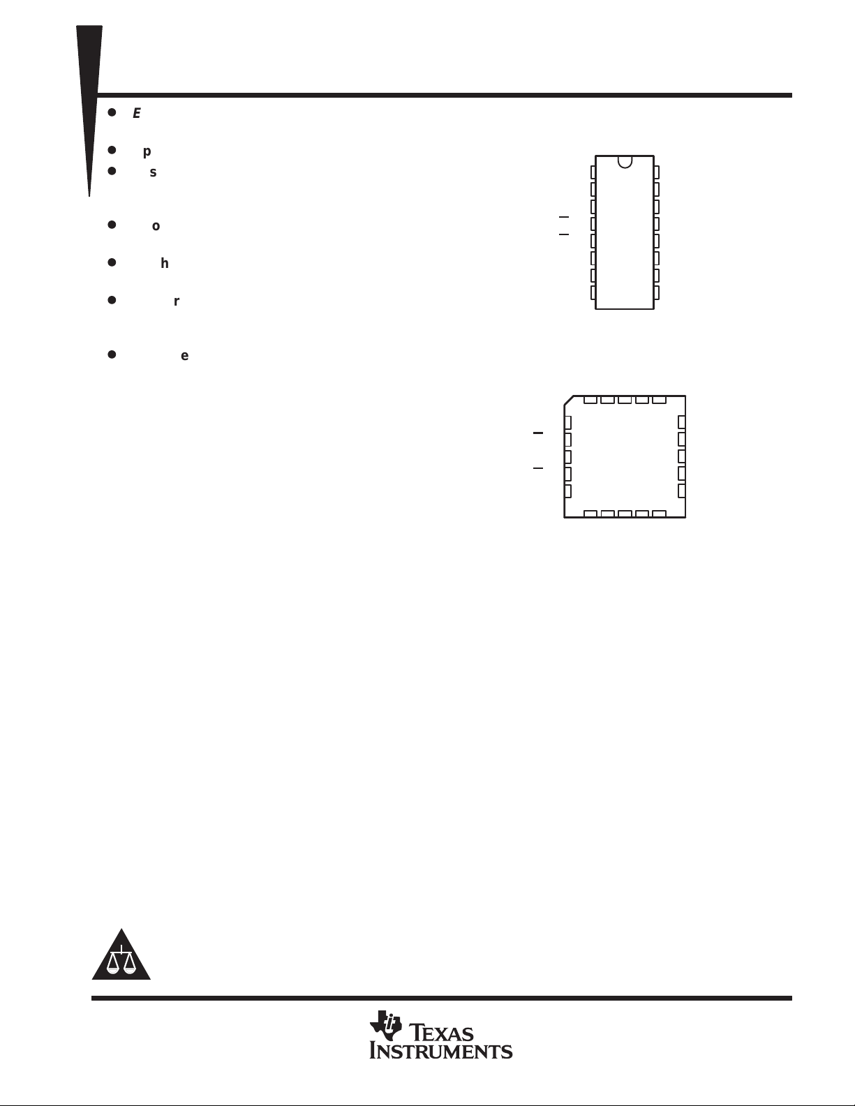
Package Options Include Plastic
Small-Outline (D), Shrink Small-Outline
(DB), Thin Very Small-Outline (DGV), Thin
Shrink Small-Outline (PW), and Ceramic
Flat (W) Packages, Ceramic Chip
Carriers (FK), and Standard Plastic (N) and
Ceramic (J) DIPs
description
The ’AHC138 decoders/demultiplexers are
designed for high-performance memory-decoding
and data-routing applications that require very
short propagation-delay times. In
high-performance memory systems, these
decoders can be used to minimize the effects of
system decoding. When employed with
high-speed memories utilizing a fast enable
circuit, the delay times of these decoders and the
enable time of the memory are usually less than
the typical access time of the memory . This means
that the effective system delay introduced by the
decoders is neg ligible.
SN54AHC138 ...J OR W PACKAGE
SN74AHC138 . . . D, DB, DGV, N, OR PW PACKAGE
SN54AHC138 . . . FK PACKAGE
C
G
2A
NC
G
2B
G1
NC – No internal connection
(TOP VIEW)
A
B
C
G
2A
G
2B
G1
Y7
GND
(TOP VIEW)
BANC
3212019
4
5
6
7
8
910111213
Y7
1
2
3
4
5
6
7
8
GND
16
15
14
13
12
11
10
NC
9
V
CC
Y6
V
Y0
Y1
Y2
Y3
Y4
Y5
Y6
Y0
18
17
16
15
14
Y5
CC
Y1
Y2
NC
Y3
Y4
The conditions at the binary-select inputs and the three enable inputs select one of eight output lines. Two
active-low and one active-high enable inputs reduce the need for external gates or inverters when expanding.
A 24-line decoder can be implemented without external inverters and a 32-line decoder requires only one
inverter. An enable input can be used as a data input for demultiplexing applications.
The SN54AHC138 is characterized for operation over the full military temperature range of –55°C to 125°C. The
SN74AHC138 is characterized for operation from –40°C to 85°C.
Please be aware that an important notice concerning availability, standard warranty, and use in critical applications of
Texas Instruments semiconductor products and disclaimers thereto appears at the end of this data sheet.
EPIC is a trademark of Texas Instruments Incorporated.
PRODUCTION DATA information is current as of publication date.
Products conform to specifications per the terms of Texas Instruments
standard warranty. Production processing does not necessarily include
testing of all parameters.
POST OFFICE BOX 655303 • DALLAS, TEXAS 75265
Copyright 2000, Texas Instruments Incorporated
On products compliant to MIL-PRF-38535, all parameters are tested
unless otherwise noted. On all other products, production
processing does not necessarily include testing of all parameters.
1
SN54AHC138, SN74AHC138
3-LINE TO 8-LINE DECODERS/DEMULTIPLEXERS
SCLS258I – DECEMBER 1995 – REVISED JANUARY 2000
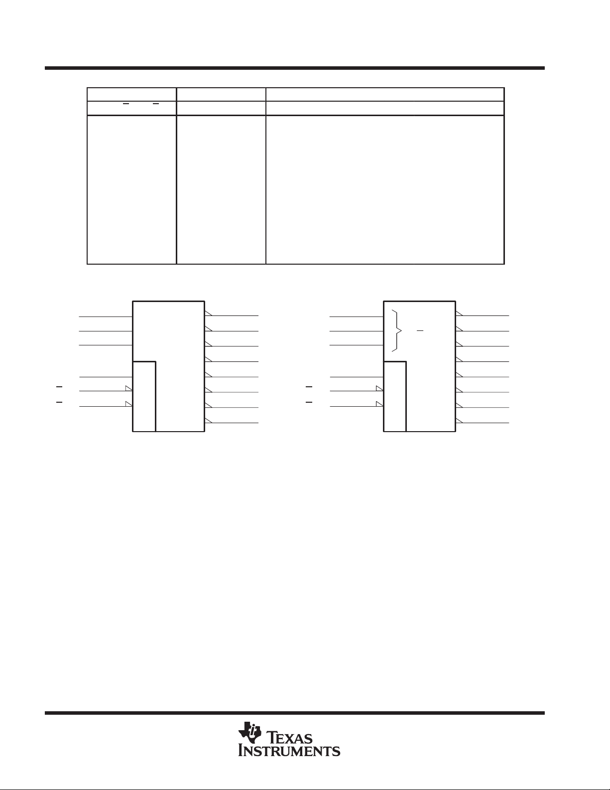
FUNCTION TABLE
ENABLE INPUTS
G1 G2A G2B C B A Y0 Y1 Y2 Y3 Y4 Y5 Y6 Y7
X H X X X X H H H H H H H H
X XHXXXHHHHHHHH
L XXXXXHHHHHHHH
H LLLLLLHHHHHHH
H LLLLHHLHHHHHH
H LLLHLHHLHHHHH
H LLLHHHHHLHHHH
H LLHLLHHHHLHHH
H LLHLHHHHHHLHH
H LLHHLHHHHHHLH
H L L H H H H H H H H H H L
SELECT INPUTS OUTPUTS
logic symbols (alternatives)
1
A
2
B
3
C
6
G1
4
G
2A
5
G2B
†
These symbols are in accordance with ANSI/IEEE Std 91-1984 and IEC Publication 617-12.
Pin numbers shown are for the D, DB, DGV, J, N, PW, and W packages.
BIN/OCT
1
2
4
&
EN
†
15
0
1
2
3
4
5
6
7
14
13
12
11
10
Y0
Y1
Y2
Y3
Y4
Y5
9
Y6
7
Y7
G1
G2A
G2B
1
A
2
B
3
C
6
4
5
DMUX
0
G
2
&
0
0
1
7
2
3
4
5
6
7
15
14
13
12
11
10
Y0
Y1
Y2
Y3
Y4
Y5
9
Y6
7
Y7
2
POST OFFICE BOX 655303 • DALLAS, TEXAS 75265
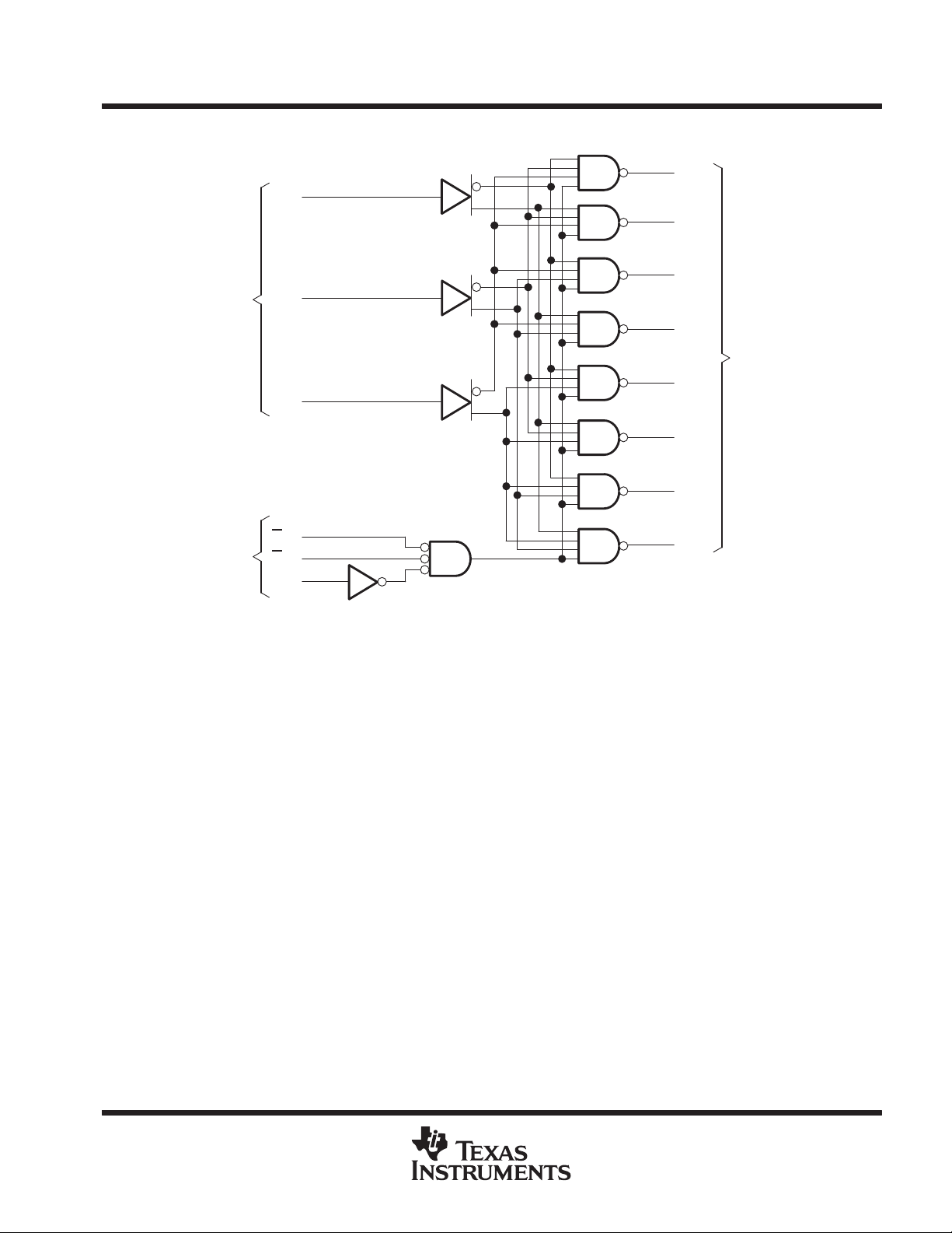
logic diagram (positive logic)
1
A
Select
Inputs
2
B
3
C
SN54AHC138, SN74AHC138
3-LINE TO 8-LINE DECODERS/DEMULTIPLEXERS
SCLS258I – DECEMBER 1995 – REVISED JANUARY 2000
15
Y0
14
Y1
13
Y2
12
Y3
Data
11
10
Y4
Y5
9
Y6
Outputs
4
G2A
Enable
Inputs
Pin numbers shown are for the D, DB, DGV, J, N, PW, and W packages.
G2B
G1
5
6
7
Y7
absolute maximum ratings over operating free-air temperature range (unless otherwise noted)
Supply voltage range, VCC –0.5 V to 7 V. . . . . . . . . . . . . . . . . . . . . . . . . . . . . . . . . . . . . . . . . . . . . . . . . . . . . . . . . .
Input voltage range, VI (see Note 1) –0.5 V to 7 V. . . . . . . . . . . . . . . . . . . . . . . . . . . . . . . . . . . . . . . . . . . . . . . . . .
Output voltage range, VO (see Note 1) –0.5 V to V
Input clamp current, I
Output clamp current, I
Continuous output current, I
(V
< 0) –20 mA. . . . . . . . . . . . . . . . . . . . . . . . . . . . . . . . . . . . . . . . . . . . . . . . . . . . . . . . . . .
IK
I
(V
OK
< 0 or VO > VCC) ±20 mA. . . . . . . . . . . . . . . . . . . . . . . . . . . . . . . . . . . . . . . . . . . .
O
(V
= 0 to VCC) ±25 mA. . . . . . . . . . . . . . . . . . . . . . . . . . . . . . . . . . . . . . . . . . . . . .
O
O
Continuous current through VCC or GND ±75 mA. . . . . . . . . . . . . . . . . . . . . . . . . . . . . . . . . . . . . . . . . . . . . . . . . . .
Package thermal impedance, θJA (see Note 2): D package 73°C/W. . . . . . . . . . . . . . . . . . . . . . . . . . . . . . . . . . .
DB package 82°C/W. . . . . . . . . . . . . . . . . . . . . . . . . . . . . . . . .
DGV package 120°C/W. . . . . . . . . . . . . . . . . . . . . . . . . . . . . . .
N package 67°C/W. . . . . . . . . . . . . . . . . . . . . . . . . . . . . . . . . . .
PW package 108°C/W. . . . . . . . . . . . . . . . . . . . . . . . . . . . . . . .
Storage temperature range, T
†
Stresses beyond those listed under “absolute maximum ratings” may cause permanent damage to the device. These are stress ratings only, and
functional operation of the device at these or any other conditions beyond those indicated under “recommended operating conditions” is not
implied. Exposure to absolute-maximum-rated conditions for extended periods may affect device reliability.
NOTES: 1. The input and output voltage ratings may be exceeded if the input and output current ratings are observed.
2. The package thermal impedance is calculated in accordance with JESD 51.
–65°C to 150°C. . . . . . . . . . . . . . . . . . . . . . . . . . . . . . . . . . . . . . . . . . . . . . . . . . .
stg
CC
+ 0.5 V. . . . . . . . . . . . . . . . . . . . . . . . . . . . . . . . . . . . . . . .
†
POST OFFICE BOX 655303 • DALLAS, TEXAS 75265
3
 Loading...