

Texas Instruments SN74ACT74D, SN74ACT74DBLE, SN74ACT74DBR, SN74ACT74DR, SN74ACT74N Datasheet
...
SN54ACT74, SN74ACT74
DUAL POSITIVE-EDGE-TRIGGERED D-TYPE FLIP-FLOPS
WITH CLEAR AND PRESET
SCAS520E – AUGUST 1995 – REVISED JANUARY 2000
D
Inputs Are TTL-Voltage Compatible
D
EPIC
(Enhanced-Performance Implanted
CMOS) 1-µm Process
D
Package Options Include Plastic
Small-Outline (DW) Shrink Small-Outline
(DB), and Thin Shrink Small-Outline (PW)
Packages, Ceramic Chip Carriers (FK) and
Flatpacks (W), and Standard Plastic (N) and
Ceramic (J) DIPs
description
The ’ACT74 dual positive-edge-triggered devices
are D-type flip-flops.
A low level at the preset (PRE
sets or resets the outputs, regardless of the levels
of the other inputs. When PRE
inactive (high), data at the data (D) input meeting
the setup-time requirements is transferred to the
outputs on the positive-going edge of the clock
pulse. Clock triggering occurs at a voltage level
and is not directly related to the rise time of the
clock pulse. Following the hold-time interval, data
at D can be changed without affecting the levels
at the outputs.
The SN54ACT74 is characterized for operation
over the full military temperature range of –55°C
to 125°C. The SN74ACT74 is characterized for
operation from –40°C to 85°C.
) or clear (CLR) input
and CLR are
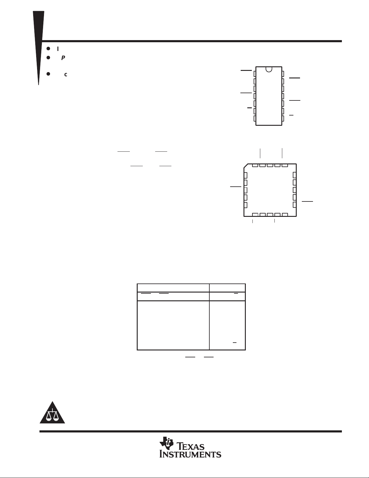
SN54ACT74 ...J OR W PACKAGE
SN74ACT74 . . . D, DB, N, OR PW PACKAGE
1CLR
1CLK
1PRE
SN54ACT74 . . . FK PACKAGE
1CLK
NC
1PRE
NC
1Q
NC – No internal connection
(TOP VIEW)
1
1D
2
3
4
1Q
5
1Q
6
GND
7
(TOP VIEW)
1D
3212019
4
5
6
7
8
910111213
1Q
1CLR
NC
NC
GND
14
13
12
11
10
9
8
CC
V
2Q
V
CC
2CLR
2D
2CLK
2PRE
2Q
2Q
2CLR
18
17
16
15
14
2Q
2D
NC
2CLK
NC
2PRE
PRE
L H X X H L
H LXXLH
L LXXH†H
H H ↑ HHL
H H ↑ LLH
H H L X Q
†
This configuration is unstable; that is, it does not
persist when either PRE
inactive (high) level.
Please be aware that an important notice concerning availability, standard warranty, and use in critical applications of
Texas Instruments semiconductor products and disclaimers thereto appears at the end of this data sheet.
EPIC is a trademark of Texas Instruments Incorporated.
PRODUCTION DATA information is current as of publication date.
Products conform to specifications per the terms of Texas Instruments
standard warranty. Production processing does not necessarily include
testing of all parameters.
FUNCTION TABLE
(each flip-flop)
INPUTS
CLR
CLK D Q Q
or CLR returns to its
OUTPUTS
Q
0
†
0
Copyright 2000, Texas Instruments Incorporated
On products compliant to MIL-PRF-38535, all parameters are tested
unless otherwise noted. On all other products, production
processing does not necessarily include testing of all parameters.
POST OFFICE BOX 655303 • DALLAS, TEXAS 75265
1
SN54ACT74, SN74ACT74
DUAL POSITIVE-EDGE-TRIGGERED D-TYPE FLIP-FLOPS
WITH CLEAR AND PRESET
SCAS520E – AUGUST 1995 – REVISED JANUARY 2000
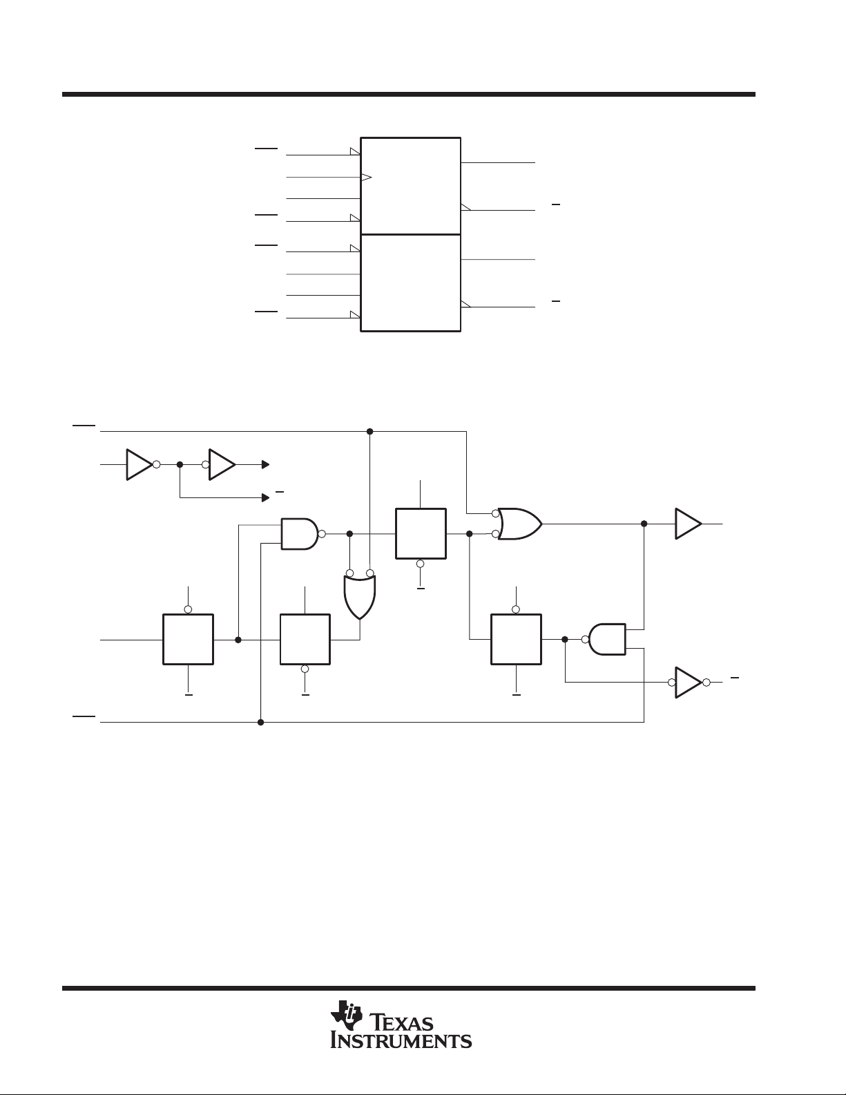
logic symbol
†
This symbol is in accordance with ANSI/IEEE Std 91-1984 and IEC Publication 617-12.
Pin numbers shown are for the D, DB, J, N, PW, and W packages.
†
1PRE
1CLK
1D
1CLR
2PRE
2CLK
2D
2CLR
4
3
2
1
10
11
12
13
S
C1
1D
R
logic diagram, each flip-flop (positive logic)
PRE
CLK
C
C
C
5
1Q
6
1Q
9
2Q
8
2Q
CLR
TG
C
D
C
C
C
C
C
TGTGTG
C
Q
Q
2
POST OFFICE BOX 655303 • DALLAS, TEXAS 75265
 Loading...