

Texas Instruments SNJ54ACT16373WD Datasheet
SN54ACT16373, 74ACT16373
16-BIT D-TYPE TRANSPARENT LATCHES
WITH 3-STATE OUTPUTS
SCAS122C – MARCH 1990 – REVISED SEPTEMBER 1996
1
POST OFFICE BOX 655303 • DALLAS, TEXAS 75265
D
Members of the Texas Instruments
Widebus
t
Family
D
Inputs Are TTL-Voltage Compatible
D
3-State Bus Driving True Outputs
D
Full Parallel Access for Loading
D
Flow-Through Architecture Optimizes
PCB Layout
D
Distributed VCC and GND Pin Configuration
Minimizes High-Speed Switching Noise
D
EPIC
t
(Enhanced-Performance Implanted
CMOS) 1-mm Process
D
500-mA Typical Latch-Up Immunity at
125°C
D
Package Options Include Shrink
Small-Outline (DL) 300-mil Packages Using
25-mil Center-to-Center Pin Spacings and
380-mil Fine-Pitch Ceramic Flat (WD)
Packages Using 25-mil Center-to-Center
Pin Spacings
description
The SN54ACT16373 and 74ACT16373 are 16-bit
D-type transparent latches with 3-state outputs
designed specifically for driving highly capacitive
or relatively low-impedance loads. They are
particularly suitable for implementing buffer
registers, I/O ports, bidirectional bus drivers, and
working registers. These devices can be used as
two 8-bit latches or one 16-bit latch. The Q outputs
of the latches follow the data (D) inputs if enable
C is taken high. When C is taken low, the Q outputs
are latched at the levels set up at the D inputs.
A buffered output-enable (OE
) input can be used to place the outputs in either a normal logic state (high or low
logic levels) or the high-impedance state. In the high-impedance state, the outputs neither load nor drive the
bus lines significantly . The high-impedance state and the increased drive provide the capability to drive bus lines
in a bus-organized system without need for interface or pullup components.
OE
does not affect the internal operations of the latches. Old data can be retained or new data can be entered
while the outputs are in the high-impedance state.
The 74ACT16373 is packaged in TI’s shrink small-outline package, which provides twice the I/O pin count and
functionality of standard small-outline packages in the same printed-circuit-board area.
The SN54ACT16373 is characterized for operation over the full military temperature range of –55°C to 125°C.
The 74ACT16373 is characterized for operation from –40°C to 85°C.
Copyright 1996, Texas Instruments Incorporated
PRODUCTION DATA information is current as of publication date.
Products conform to specifications per the terms of Texas Instruments
standard warranty. Production processing does not necessarily include
testing of all parameters.
Please be aware that an important notice concerning availability, standard warranty, and use in critical applications of
Texas Instruments semiconductor products and disclaimers thereto appears at the end of this data sheet.
EPIC and Widebus are trademarks of Texas Instruments Incorporated.
1
2
3
4
5
6
7
8
9
10
11
12
13
14
15
16
17
18
19
20
21
22
23
24
48
47
46
45
44
43
42
41
40
39
38
37
36
35
34
33
32
31
30
29
28
27
26
25
1OE
1Q1
1Q2
GND
1Q3
1Q4
V
CC
1Q5
1Q6
GND
1Q7
1Q8
2Q1
2Q2
GND
2Q3
2Q4
V
CC
2Q5
2Q6
GND
2Q7
2Q8
2OE
1C
1D1
1D2
GND
1D3
1D4
V
CC
1D5
1D6
GND
1D7
1D8
2D1
2D2
GND
2D3
2D4
V
CC
2D5
2D6
GND
2D7
2D8
2C
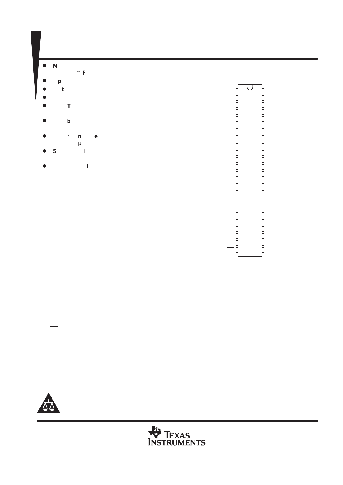
SN54ACT16373 . . . WD PACKAGE
74ACT16373 . . . DL PACKAGE
(TOP VIEW)
SN54ACT16373, 74ACT16373
16-BIT D-TYPE TRANSPARENT LATCHES
WITH 3-STATE OUTPUTS
SCAS122C – MARCH 1990 – REVISED SEPTEMBER 1996
2
POST OFFICE BOX 655303 • DALLAS, TEXAS 75265
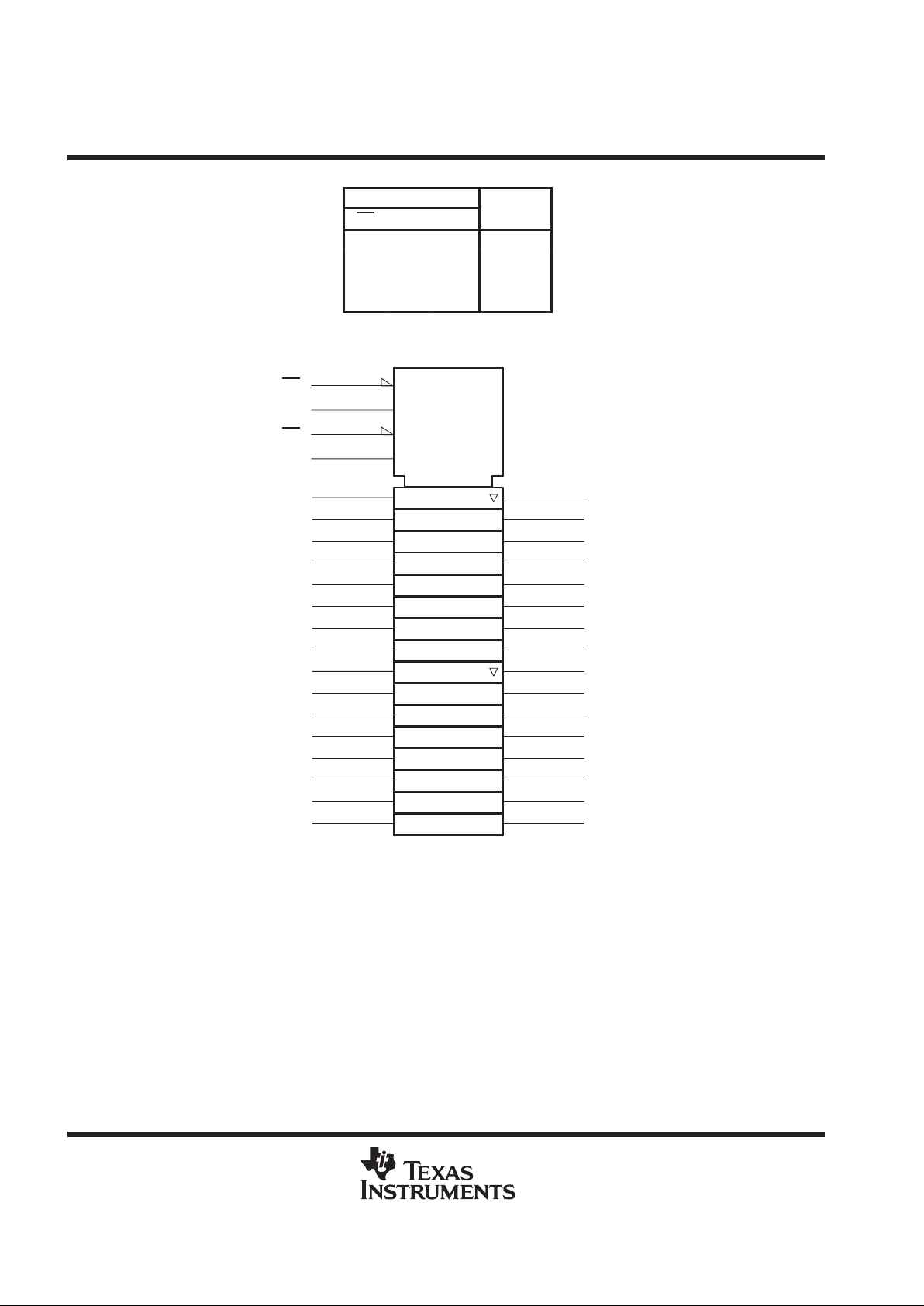
FUNCTION TABLE
INPUTS
OUTPUT
OE C
D
Q
L H H H
L HL L
L LX Q
0
H X X Z
logic symbol
†
†
This symbol is in accordance with ANSI/IEEE Std 91-1984 and IEC Publication 617-12.
1OE
2OE
1EN
1
C1
48
1C
1D
47
1D1
46
1D2
44
1D3
43
1D4
1Q1
2
1Q2
3
1Q3
5
1Q4
6
2
41
1D5
40
1D6
38
1D7
37
1D8
1Q5
8
1Q6
9
1Q7
11
1Q8
12
3D
36
2D1
35
2D2
33
2D3
32
2D4
2Q1
13
2Q2
14
2Q3
16
2Q4
17
30
2D5
29
2D6
27
2D7
26
2D8
2Q5
19
2Q6
20
2Q7
22
2Q8
23
4
2EN
24
C4
25
2C
1
1
 Loading...