

Texas Instruments SN74ACT14D, SN74ACT14DBLE, SN74ACT14DBR, SN74ACT14DR, SN74ACT14N Datasheet
...
SN54ACT14, SN74ACT14
HEX SCHMITT-TRIGGER INVERTER
SCAS557E – DECEMBER 1995 – REVISED JANUARY 2000
1
POST OFFICE BOX 655303 • DALLAS, TEXAS 75265
D
Inputs Are TTL-Voltage Compatible
D
EPIC
(Enhanced-Performance Implanted
CMOS) 1-µm Process
D
Package Options Include Plastic
Small-Outline (D), Shrink Small-Outline
(DB), and Thin-Shrink Small-Outline (PW)
Packages, Ceramic Chip Carriers (FK) and
Flatpacks (W), and Standard Plastic (N) and
Ceramic (J) DIPs
description
These Schmitt-trigger devices contain six
independent inverters. They perform the Boolean
function Y = A. Because of the Schmitt action, they
have different input threshold levels for
positive-going (VT+) and for negative-going (VT–)
signals.
These circuits are temperature compensated and
can be triggered from the slowest of input ramps
and still give clean, jitter-free output signals. They
also have a greater noise margin than
conventional inverters.
SN54ACT14 is characterized for operation over
the full military temperature range of –55°C to
125°C. The SN74ACT14 is characterized for
operation from –40°C to 85°C.
FUNCTION TABLE
(each inverter)
INPUTAOUTPUT
Y
H L
L H
Copyright 2000, Texas Instruments Incorporated
PRODUCTION DATA information is current as of publication date.
Products conform to specifications per the terms of Texas Instruments
standard warranty. Production processing does not necessarily include
testing of all parameters.
On products compliant to MIL-PRF-38535, all parameters are tested
unless otherwise noted. On all other products, production
processing does not necessarily include testing of all parameters.
EPIC is a trademark of Texas Instruments Incorporated.
Please be aware that an important notice concerning availability, standard warranty, and use in critical applications of
Texas Instruments semiconductor products and disclaimers thereto appears at the end of this data sheet.
1
2
3
4
5
6
7
14
13
12
11
10
9
8
1A
1Y
2A
2Y
3A
3Y
GND
V
CC
6A
6Y
5A
5Y
4A
4Y
3212019
910111213
4
5
6
7
8
18
17
16
15
14
6Y
NC
5A
NC
5Y
2A
NC
2Y
NC
3A
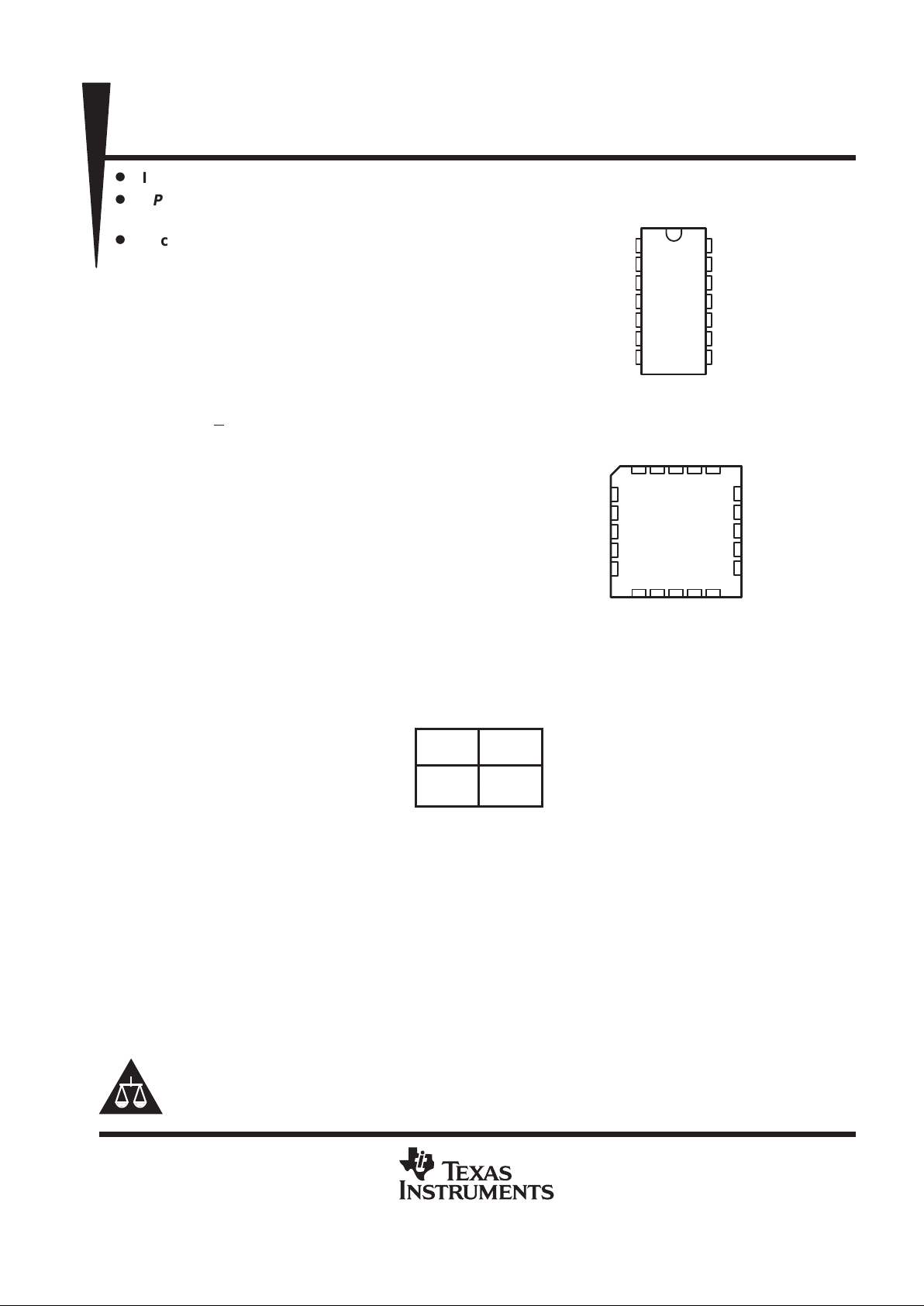
SN54ACT14 . . . FK PACKAGE
(TOP VIEW)
1Y1ANC
4Y
4A
V
6A
3Y
GND
NC
CC
SN54ACT14 ...J OR W PACKAGE
SN74ACT14 . . . D, DB, N, OR PW PACKAGE
(TOP VIEW)
NC – No internal connection
SN54ACT14, SN74ACT14
HEX SCHMITT-TRIGGER INVERTER
SCAS557E – DECEMBER 1995 – REVISED JANUARY 2000
2
POST OFFICE BOX 655303 • DALLAS, TEXAS 75265
logic symbol
†
†
This symbol is in accordance with ANSI/IEEE Std 91-1984 and
IEC Publication 617-12.
Pin numbers shown are for the D, DB, J, N, PW, or W packages.
1
1A
3
2A
5
3A
9
4A
11
5A
13
6A
1Y
2
3Y
6
2Y
4
4Y
8
6Y
12
5Y
10
logic diagram (positive logic)
AY
absolute maximum ratings over operating free-air temperature range (unless otherwise noted)
‡
Supply voltage range, VCC –0.5 V to 7 V. . . . . . . . . . . . . . . . . . . . . . . . . . . . . . . . . . . . . . . . . . . . . . . . . . . . . . . . . .
Input voltage range, VI (see Note 1) –0.5 V to VCC + 0.5 V. . . . . . . . . . . . . . . . . . . . . . . . . . . . . . . . . . . . . . . . . . .
Output voltage range, VO (see Note 1) –0.5 V to VCC + 0.5 V. . . . . . . . . . . . . . . . . . . . . . . . . . . . . . . . . . . . . . . .
Input clamp current, IIK (VI < 0 or VI > VCC) ±20 mA. . . . . . . . . . . . . . . . . . . . . . . . . . . . . . . . . . . . . . . . . . . . . . . .
Output clamp current, IOK (VO < 0 or VO > VCC) ±20 mA. . . . . . . . . . . . . . . . . . . . . . . . . . . . . . . . . . . . . . . . . . . .
Continuous output current, I
O
(VO = 0 to VCC) ±50 mA. . . . . . . . . . . . . . . . . . . . . . . . . . . . . . . . . . . . . . . . . . . . . .
Continuous current through VCC or GND ±200 mA. . . . . . . . . . . . . . . . . . . . . . . . . . . . . . . . . . . . . . . . . . . . . . . . . .
Package thermal impedance, θJA (see Note 2): D package 86°C/W. . . . . . . . . . . . . . . . . . . . . . . . . . . . . . . . . . .
DB package 96°C/W. . . . . . . . . . . . . . . . . . . . . . . . . . . . . . . . .
N package 80°C/W. . . . . . . . . . . . . . . . . . . . . . . . . . . . . . . . . . .
PW package 113°C/W. . . . . . . . . . . . . . . . . . . . . . . . . . . . . . . .
Storage temperature range, T
stg
–65°C to 150°C. . . . . . . . . . . . . . . . . . . . . . . . . . . . . . . . . . . . . . . . . . . . . . . . . . .
‡
Stresses beyond those listed under “absolute maximum ratings” may cause permanent damage to the device. These are stress ratings only, and
functional operation of the device at these or any other conditions beyond those indicated under “recommended operating conditions” is not
implied. Exposure to absolute-maximum-rated conditions for extended periods may affect device reliability.
NOTES: 1. The input and output voltage ratings may be exceeded if the input and output current ratings are observed.
2. The package thermal impedance is calculated in accordance with JESD 51.
recommended operating conditions (see Note 3)
SN54ACT14 SN74ACT14
MIN MAX MIN MAX
UNIT
V
CC
Supply voltage 4.5 5.5 4.5 5.5 V
V
IH
High-level input voltage 2.1 2.1 V
V
IL
Low-level input voltage 0.5 0.5 V
V
I
Input voltage 0 V
CC
0 V
CC
V
V
O
Output voltage 0 V
CC
0 V
CC
V
I
OH
High-level output current –24 –24 mA
I
OL
Low-level output current 24 24 mA
T
A
Operating free-air temperature –55 125 –40 85 °C
NOTE 3: All unused inputs of the device must be held at VCC or GND to ensure proper device operation. Refer to the TI application report,
Implications of Slow or Floating CMOS Inputs
, literature number SCBA004.
 Loading...