

Texas Instruments SN74AC245N, SN74AC245PWLE, SN74AC245PWR, SN74AC245DBLE, SN74AC245DBR Datasheet
...
OPERATION
SN54AC245, SN74AC245
OCTAL BUS TRANSCEIVERS
WITH 3-STATE OUTPUTS
SCAS461D – FEBRUARY 1995 – REVISED DECEMBER 1996
D
EPIC
t
(Enhanced-Performance Implanted
CMOS) 1-mm Process
D
Package Options Include Plastic
Small-Outline (DW), Shrink Small-Outline
(DB), and Thin Shrink Small-Outline (PW)
Packages, Ceramic Chip Carriers (FK), and
Flatpacks (W), and Standard Plastic (N) and
Ceramic (J) DIPs
description
The ’AC245 octal bus transceivers are designed
for asynchronous two-way communication
between data buses. The control-function
implementation minimizes external timing
requirements.
When the output-enable (OE
passes noninverted data from the A bus to the B
bus or from the B bus to the A bus, depending on
the logic level at the direction control (DIR) input.
A high on OE disables the device so that the buses
are effectively isolated.
The SN54AC245 is characterized for operation
over the full military temperature range of –55°C
to 125°C. The SN74AC245 is characterized for
operation from –40°C to 85°C.
) is low, the device
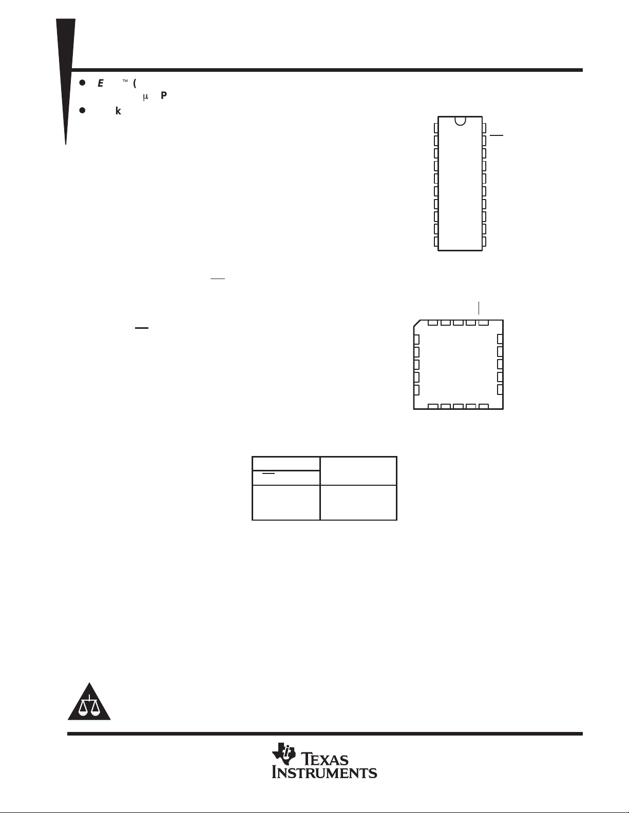
SN54AC245 ...J OR W PACKAGE
SN74AC245 . . . DB, DW, N, OR PW PACKAGE
SN54AC245 . . . FK PACKAGE
A3
A4
A5
A6
A7
(TOP VIEW)
DIR
A1
A2
A3
A4
A5
A6
A7
A8
GND
(TOP VIEW)
A2A1DIR
3 2 1 20 19
4
5
6
7
8
9 10 11 12 13
1
2
3
4
5
6
7
8
9
10
20
19
18
17
16
15
14
13
12
11
V
CC
18
17
16
15
14
V
OE
B1
B2
B3
B4
B5
B6
B7
B8
CC
B1
B2
B3
B4
B5
B7
B8
B6 OE
A8
GND
FUNCTION TABLE
INPUTS
OE
Please be aware that an important notice concerning availability, standard warranty, and use in critical applications of
Texas Instruments semiconductor products and disclaimers thereto appears at the end of this data sheet.
DIR
L
L
H
L
H
X
B data to A bus
A data to B bus
Isolation
EPIC is a trademark of Texas Instruments Incorporated.
PRODUCTION DATA information is current as of publication date.
Products conform to specifications per the terms of Texas Instruments
standard warranty. Production processing does not necessarily include
testing of all parameters.
POST OFFICE BOX 655303 • DALLAS, TEXAS 75265
Copyright 1996, Texas Instruments Incorporated
1
SN54AC245, SN74AC245
OCTAL BUS TRANSCEIVERS
WITH 3-STATE OUTPUTS
SCAS461D – FEBRUARY 1995 – REVISED DECEMBER 1996
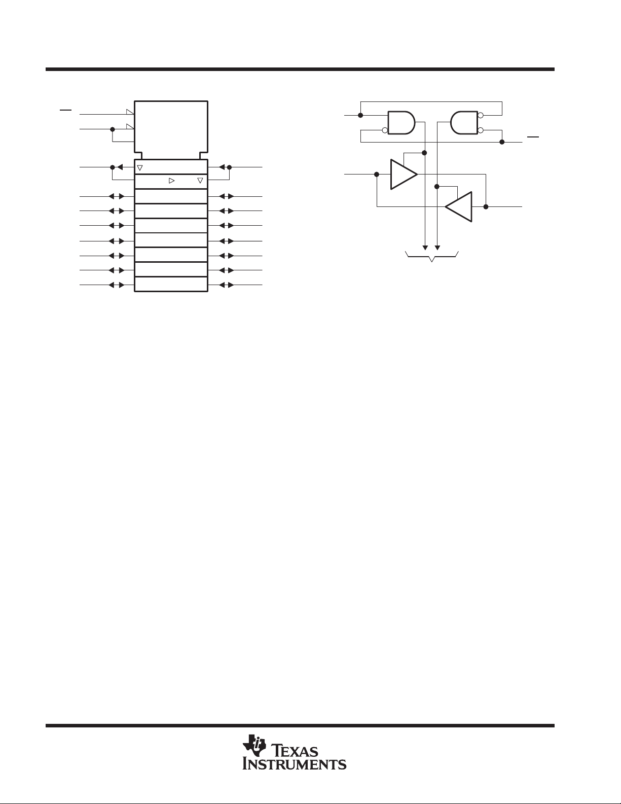
logic symbol
19
OE
1
DIR
2
A1
3
A2
4
A3
5
A4
6
A5
7
A6
8
A7
9
A8
†
This symbol is in accordance with ANSI/IEEE Std 91-1984 and
IEC Publication 617-12.
†
G3
3EN1[BA]
3EN2[AB]
1
18
2
17
16
15
14
13
12
11
B1
B2
B3
B4
B5
B6
B7
B8
logic diagram (positive logic)
1
DIR
2
A1
To Seven Other Channels
19
18
OE
B1
absolute maximum ratings over operating free-air temperature range (unless otherwise noted)
Supply voltage range, V
CC
Input voltage range, VI (see Note 1) –0.5 V to VCC+ 0.5 V. . . . . . . . . . . . . . . . . . . . . . . . . . . . . . . . . . . . . . . . . . .
Output voltage range, VO (see Note 1) –0.5 V to VCC+ 0.5 V. . . . . . . . . . . . . . . . . . . . . . . . . . . . . . . . . . . . . . . .
Input clamp current, I
Output clamp current, I
Continuous output current, I
(V
< 0 or VI > VCC) ±20 mA. . . . . . . . . . . . . . . . . . . . . . . . . . . . . . . . . . . . . . . . . . . . . . . . .
IK
I
(V
< 0 or VO > VCC) ±20 mA. . . . . . . . . . . . . . . . . . . . . . . . . . . . . . . . . . . . . . . . . . . .
OK
O
(V
= 0 to VCC) ±50 mA. . . . . . . . . . . . . . . . . . . . . . . . . . . . . . . . . . . . . . . . . . . . . .
O
O
Continuous current through VCC or GND ±200 mA. . . . . . . . . . . . . . . . . . . . . . . . . . . . . . . . . . . . . . . . . . . . . . . . . .
Maximum power dissipation at TA = 55°C (in still air)(see Note 2): DB package 0.6 W. . . . . . . . . . . . . . . . . . .
DW package 1.6 W. . . . . . . . . . . . . . . . . .
N package 1.3 W. . . . . . . . . . . . . . . . . . . .
PW package 0.7 W. . . . . . . . . . . . . . . . . . .
Storage temperature range, T
‡
Stresses beyond those listed under “absolute maximum ratings” may cause permanent damage to the device. These are stress ratings only, and
functional operation of the device at these or any other conditions beyond those indicated under “recommended operating conditions” is not
implied. Exposure to absolute-maximum-rated conditions for extended periods may affect device reliability.
NOTES: 1. The input and output voltage ratings may be exceeded if the input and output current ratings are observed.
2. The maximum package power dissipation is calculated using a junction temperature of 150°C and a board trace length of 750 mils,
except for the N package, which has a trace length of zero.
stg
–0.5 V to 7 V. . . . . . . . . . . . . . . . . . . . . . . . . . . . . . . . . . . . . . . . . . . . . . . . . . . . . . . . . .
–65°C to 150°C. . . . . . . . . . . . . . . . . . . . . . . . . . . . . . . . . . . . . . . . . . . . . . . . . . . .
‡
2
POST OFFICE BOX 655303 • DALLAS, TEXAS 75265
 Loading...