

Texas Instruments SN74ABT843DBLE, SN74ABT843DBR, SN74ABT843DW, SN74ABT843DWR, SN74ABT843NT Datasheet
...
SN54ABT843, SN74ABT843
9-BIT BUS-INTERFACE D-TYPE LATCHES
WITH 3-STATE OUTPUTS
SCBS197D – FEBRUARY 1991 – REVISED MAY 1997
D
State-of-the-Art
EPIC-ΙΙB
BiCMOS Design
Significantly Reduces Power Dissipation
D
Latch-Up Performance Exceeds 500 mA Per
JEDEC Standard JESD-17
D
T ypical V
(Output Ground Bounce) < 1 V
OLP
at VCC = 5 V, TA = 25°C
D
High-Drive Outputs (–32-mA IOH, 64-mA IOL)
D
Package Options Include Plastic
Small-Outline (DW) and Shrink
Small-Outline (DB) Packages, Ceramic Chip
Carriers (FK), Ceramic Flat (W) Package,
and Plastic (NT) and Ceramic (JT) DIPs
description
The ’ABT843 9-bit latches are designed
specifically for driving highly capacitive or
relatively low-impedance loads. They are
particularly suitable for implementing buffer
registers, I/O ports, bidirectional bus drivers, and
working registers.
The nine transparent D-type latches provide true
data at the outputs.
A buffered output-enable (OE) input can be used
to place the nine outputs in either a normal logic
state (high or low logic levels) or a
high-impedance state. The outputs are also in the
high-impedance state during power-up and
power-down conditions. The outputs remain in the
high-impedance state while the device is powered
down. In the high-impedance state, the outputs
neither load nor drive the bus lines significantly.
The high-impedance state and increased drive
provide the capability to drive bus lines without
need for interface or pullup components.
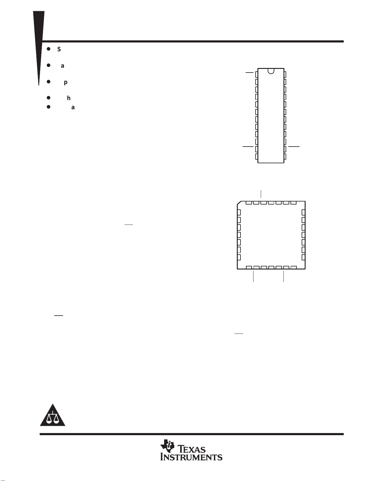
SN54ABT843 . . . JT OR W PACKAGE
SN74ABT843 . . . DB, DW, OR NT P ACKAGE
SN54ABT843 . . . FK PACKAGE
3D
4D
5D
NC
6D
7D
8D
NC – No internal connection
(TOP VIEW)
1
OE
1D
2D
3D
4D
5D
6D
7D
8D
9D
CLR
GND
(TOP VIEW)
2D1DOE
426
3212827
5
6
7
8
9
10
11
12 13
9D
24
2
23
3
22
4
21
5
20
6
19
7
18
8
17
9
16
10
15
11
14
12
13
CC
NC
V
14 15 16 17 18
LE
NC
CLR
GND
V
CC
1Q
2Q
3Q
4Q
5Q
6Q
7Q
8Q
9Q
PRE
LE
1Q
PRE
2Q
25
24
23
22
21
20
19
9Q
3Q
4Q
5Q
NC
6Q
7Q
8Q
OE
does not affect the internal operations of the latch. Previously stored data can be retained or new data can
be entered while the outputs are in the high-impedance state.
T o ensure the high-impedance state during power up or power down, OE
should be tied to VCC through a pullup
resistor; the minimum value of the resistor is determined by the current-sinking capability of the driver.
The SN54ABT843 is characterized for operation over the full military temperature range of –55°C to 125°C. The
SN74ABT843 is characterized for operation from –40°C to 85°C.
Please be aware that an important notice concerning availability, standard warranty, and use in critical applications of
Texas Instruments semiconductor products and disclaimers thereto appears at the end of this data sheet.
EPIC-ΙΙB is a trademark of Texas Instruments Incorporated.
PRODUCTION DATA information is current as of publication date.
Products conform to specifications per the terms of Texas Instruments
standard warranty. Production processing does not necessarily include
testing of all parameters.
POST OFFICE BOX 655303 • DALLAS, TEXAS 75265
Copyright 1997, Texas Instruments Incorporated
1
SN54ABT843, SN74ABT843
9-BIT BUS-INTERFACE D-TYPE LATCHES
WITH 3-STATE OUTPUTS
SCBS197D – FEBRUARY 1991 – REVISED MAY 1997
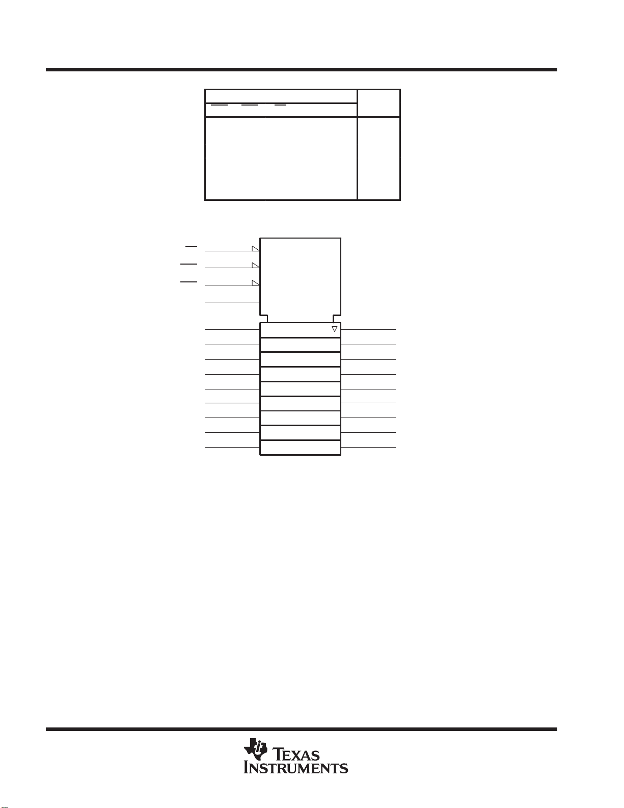
FUNCTION TABLE
INPUTS
PRE CLR OE LE D
L X L X X H
H LLXX L
H HLHL L
H HLHH H
H HLLX Q
X X H X X Z
OUTPUT
Q
0
logic symbol
†
This symbol is in accordance with ANSI/IEEE Std 91-1984 and IEC Publication 617-12.
Pin numbers shown are for the DB, DW, JT, NT, and W packages.
†
OE
PRE
CLR
LE
1D
2D
3D
4D
5D
6D
7D
8D
9D
1
14
11
13
2
3
4
5
6
7
8
9
10
EN
S2
R
C1
1D
2
23
22
21
20
19
18
17
16
15
1Q
2Q
3Q
4Q
5Q
6Q
7Q
8Q
9Q
2
POST OFFICE BOX 655303 • DALLAS, TEXAS 75265
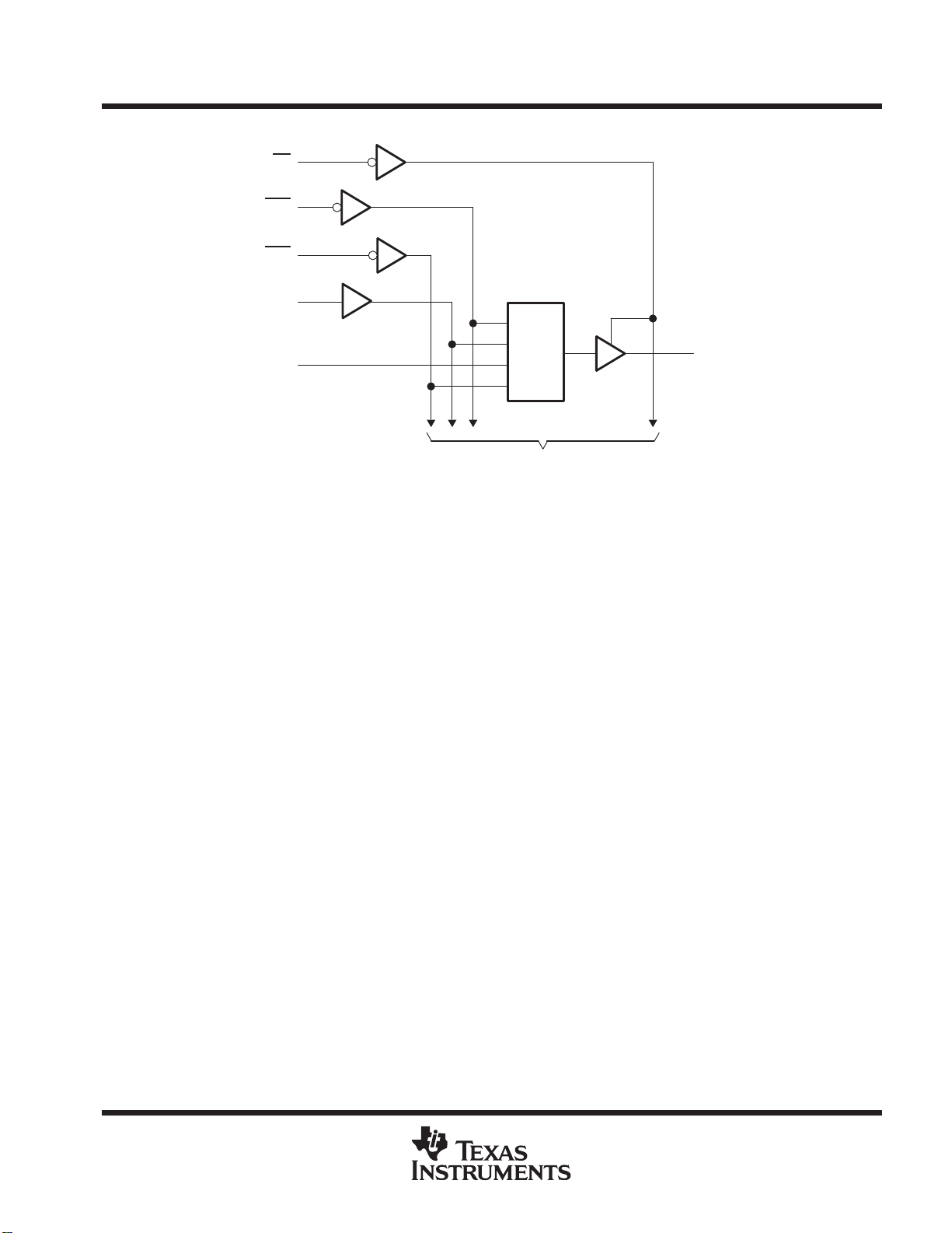
logic diagram (positive logic)
1
OE
14
PRE
11
CLR
13
LE
2
1D
Pin numbers shown are for the DB, DW, JT, NT, and W packages.
9-BIT BUS-INTERFACE D-TYPE LATCHES
S2
C1
1D
R
To Eight Other Channels
SN54ABT843, SN74ABT843
WITH 3-STATE OUTPUTS
SCBS197D – FEBRUARY 1991 – REVISED MAY 1997
23
1Q
absolute maximum ratings over operating free-air temperature range (unless otherwise noted)
Supply voltage range , VCC –0.5 V to 7 V. . . . . . . . . . . . . . . . . . . . . . . . . . . . . . . . . . . . . . . . . . . . . . . . . . . . . . . . .
Input voltage range, VI (see Note 1) –0.5 V to 7 V. . . . . . . . . . . . . . . . . . . . . . . . . . . . . . . . . . . . . . . . . . . . . . . . . .
Voltage range applied to any output in the high or power-off state, V
Current into any output in the low state, I
: SN54ABT843 96 mA. . . . . . . . . . . . . . . . . . . . . . . . . . . . . . . . . . . . .
O
SN74ABT843 128 mA. . . . . . . . . . . . . . . . . . . . . . . . . . . . . . . . . . . . .
Input clamp current, IIK (VI < 0) –18 mA. . . . . . . . . . . . . . . . . . . . . . . . . . . . . . . . . . . . . . . . . . . . . . . . . . . . . . . . . . .
Output clamp current, IOK (VO < 0) –50 mA. . . . . . . . . . . . . . . . . . . . . . . . . . . . . . . . . . . . . . . . . . . . . . . . . . . . . . . .
Package thermal impedance, θJA (see Note 2): DB package 104°C/W. . . . . . . . . . . . . . . . . . . . . . . . . . . . . . . . .
DW package 81°C/W. . . . . . . . . . . . . . . . . . . . . . . . . . . . . . . . .
NT package 67°C/W. . . . . . . . . . . . . . . . . . . . . . . . . . . . . . . . . .
Storage temperature range, T
†
Stresses beyond those listed under “absolute maximum ratings” may cause permanent damage to the device. This is a stress rating only, and
functional operation of the device at these or any other conditions beyond those indicated in the “recommended operating conditions” section of
this specification is not implied. Exposure to absolute-maximum-rated conditions for extended periods may affect device reliability .
NOTES: 1. The input and output negative-voltage ratings may be exceeded if the input and output clamp-current ratings are observed.
2. The package thermal impedance is calculated in accordance with EIA/JEDEC Std JESD51, except for through-hole packages,
which use a trace length of zero.
–65°C to 150°C. . . . . . . . . . . . . . . . . . . . . . . . . . . . . . . . . . . . . . . . . . . . . . . . . . .
stg
–0.5 V to 5.5 V. . . . . . . . . . . . . . . . . . .
O
†
POST OFFICE BOX 655303 • DALLAS, TEXAS 75265
3
 Loading...