

Texas Instruments SNJ54ABT7819GB Datasheet
SN54ABT7819
512 × 18 × 2
CLOCKED BIDIRECTIONAL FIRST-IN, FIRST-OUT MEMORY
SGBS305D – AUGUST 1994 – REVISED APRIL 1998
1
POST OFFICE BOX 655303 • DALLAS, TEXAS 75265
D
Member of the Texas Instruments
Widebus Family
D
Advanced BiCMOS Technology
D
Free-Running CLKA and CLKB Can Be
Asynchronous or Coincident
D
Read and Write Operations Synchronized
to Independent System Clocks
D
Two Separate 512 × 18 Clocked FIFOs
Buffering Data in Opposite Directions
D
IRA and ORA Synchronized to CLKA
D
IRB and ORB Synchronized to CLKB
D
Microprocessor Interface Control Logic
D
Programmable Almost-Full/Almost-Empty
Flag
D
Fast Access Times of 9 ns With a 50-pF
Load and Simultaneous-Switching Data
Outputs
D
Released as DSCC SMD (Standard
Microcircuit Drawing) 5962-9470401QXA
and 5962-9470401QYA
D
Package Options Include 84-Pin Ceramic
Pin Grid Array (GB) and 84-Pin Ceramic
Quad Flat (HT) Package
AF/AEB
HFB
IRB
GND
B0
B1
V
CC
B2
B3
GND
NC
B4
B5
GND
B6
B7
GND
B8
B9
V
CC
B10
AF/AEA
HFA
IRA
GND
A0
A1
V
CC
A2
A3
GND
NC
A4
A5
GND
A6
A7
GND
A8
A9
V
CC
A10
HT PACKAGE
(TOP VIEW)
NC
CSA
W/RA
GND
WENA
CLKA
RENA
ORA
NC
B16
A13
A14
A15
GND
A16
A1 1
ORB
GND
B15
B14
RENB
CLKB
WENB
GND
PENA
B13
B12
B1 1
W/RB
CSB
PENB
GND
CC
V
A17
B17
GND
RSTA
RSTB
1
2
3
4
5
6
7
8
9
10
11
12
13
14
15
16
17
18
19
20
21
22 23 24 25 26 27 28 29 30 31 32 33 34 35 36 37 38 39 40 41 42
63
62
61
60
59
58
57
56
55
54
53
52
51
50
49
48
47
46
45
44
43
79 78 77 76 7580 74 72 71 7073 69 68 67 66 65 6484 82 8183
CC
V
CC
V
CC
V
A12
PRODUCTION DATA information is current as of publication date.
Products conform to specifications per the terms of Texas Instruments
standard warranty. Production processing does not necessarily include
testing of all parameters.
Copyright 1998, Texas Instruments Incorporated
Widebus is a trademark of Texas Instruments Incorporated.
Please be aware that an important notice concerning availability, standard warranty, and use in critical applications of
Texas Instruments semiconductor products and disclaimers thereto appears at the end of this data sheet.
On products compliant to MIL-PRF-38535, all parameters are tested
unless otherwise noted. On all other products, production
processing does not necessarily include testing of all parameters.
SN54ABT7819
512 × 18 × 2
CLOCKED BIDIRECTIONAL FIRST-IN, FIRST-OUT MEMORY
SGBS305D – AUGUST 1994 – REVISED APRIL 1998
2
POST OFFICE BOX 655303 • DALLAS, TEXAS 75265
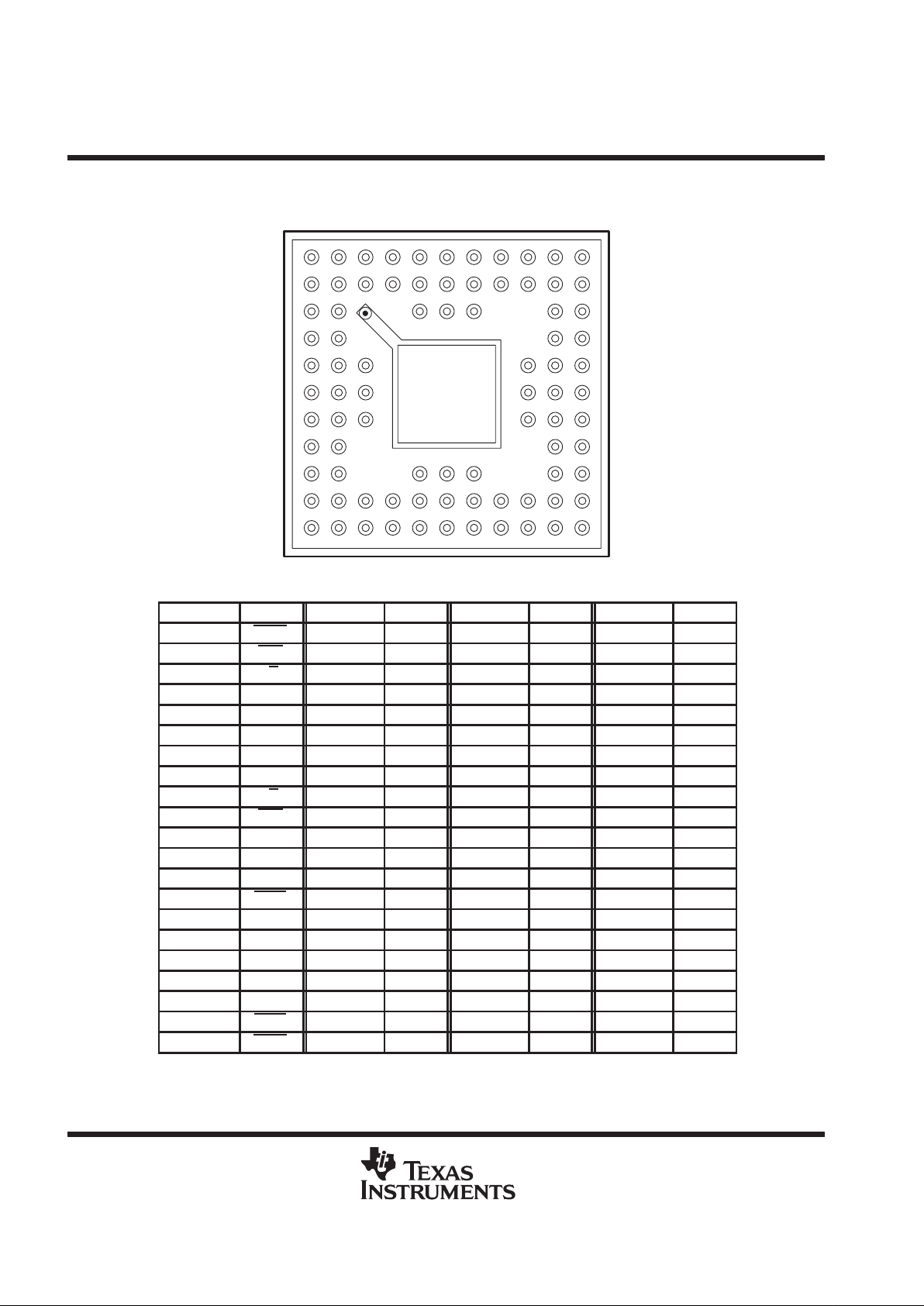
GB PACKAGE
(TOP VIEW)
A
B
C
D
E
F
G
H
J
K
L
1234567891011
Terminal Assignments
TERMINAL NAME TERMINAL NAME TERMINAL NAME TERMINAL NAME
A1 PENA B11 IRB F9 NC K2 A11
A2 CSA C1 GND F10 B6 K3 GND
A3 W/RA C2 HFA F11 GND K4 V
CC
A4 WENA C5 CLKA G1 A5 K5 GND
A5 ORA C6 NC G2 GND K6 A17
A6 V
CC
C7 V
CC
G3 A4 K7 GND
A7 ORB C10 HFB G9 B4 K8 V
CC
A8 WENB C11 GND G10 GND K9 GND
A9 W/RB D1 A1 G11 B5 K10 B10
A10 CSB D2 A0 H1 A7 K11 B9
A11 AF/AEB D10 B0 H2 GND L1 A10
B1 IRA D11 B1 H10 GND L2 A12
B2 AF/AEA E1 A3 H11 B7 L3 A13
B3 RSTA E2 A2 J1 A8 L4 A14
B4 GND E3 V
CC
J2 V
CC
L5 A16
B5 RENA E9 V
CC
J5 A15 L6 B15
B6 CLKB E10 B2 J6 NC L7 B16
B7 RENB E11 B3 J7 B17 L8 B14
B8 GND F1 A6 J10 V
CC
L9 B13
B9 RSTB F2 GND J11 B8 L10 B12
B10 PENB F3 NC K1 A9 L11 B11

SN54ABT7819
512 × 18 × 2
CLOCKED BIDIRECTIONAL FIRST-IN, FIRST-OUT MEMORY
SGBS305D – AUGUST 1994 – REVISED APRIL 1998
3
POST OFFICE BOX 655303 • DALLAS, TEXAS 75265
description
A FIFO memory is a storage device that allows data to be read from its array in the same order it is written. The
SN54ABT7819 is a high-speed, low-power BiCMOS bidirectional clocked FIFO memory. Two independent
512 × 18 dual-port SRAM FIFOs on the chip buffer data in opposite directions. Each FIFO has flags to indicate
empty and full conditions, a half-full flag, and a programmable almost-full/almost-empty flag.
The SN54ABT7819 is a clocked FIFO, which means each port employs a synchronous interface. All data
transfers through a port are gated to the low-to-high transition of a continuous (free-running) port clock by enable
signals. The continuous clocks for each port are independent of one another and can be asynchronous or
coincident. The enables for each port are arranged to provide a simple bidirectional interface between
microprocessors and/or buses with synchronous control.
The state of the A0–A17 outputs is controlled by CSA
and W/RA. When both CSA and W/RA are low, the outputs
are active. The A0–A17 outputs are in the high-impedance state when either CSA
or W/RA is high. Data is
written to FIFOA–B from port A on the low-to-high transition of CLKA when CSA
is low, W/RA is high, WENA
is high, and the IRA flag is high. Data is read from FIFOB–A to the A0–A17 outputs on the low-to-high transition
of CLKA when CSA
is low, W/RA is low, RENA is high, and the ORA flag is high.
The state of the B0–B17 outputs is controlled by CSB
and W/RB. When both CSB and W/RB are low, the outputs
are active. The B0–B17 outputs are in the high-impedance state when either CSB
or W/RB is high. Data is
written to FIFOB–A from port B on the low-to-high transition of CLKB when CSB
is low, W/RB is high, WENB
is high, and the IRB flag is high. Data is read from FIFOA–B to the B0–B17 outputs on the low-to-high transition
of CLKB when CSB
is low, W/RB is low, RENB is high, and the ORB flag is high.
The setup- and hold-time constraints for the chip selects (CSA
, CSB) and write/read selects (W/RA, W/RB)
enable and read operations on memory and are not related to the high-impedance control of the data outputs.
If a port read enable (RENA or RENB) and write enable (WENA or WENB) are set low during a clock cycle, the
chip select and write/read select can switch at any time during the cycle to change the state of the data outputs.
The input-ready and output-ready flags of a FIFO are two-stage synchronized to the port clocks for use as
reliable control signals. CLKA synchronizes the status of the input-ready flag of FIFOA–B (IRA) and the
output-ready flag of FIFOB–A (ORA). CLKB synchronizes the status of the input-ready flag of FIFOB–A (IRB)
and the output-ready flag of FIFOA–B (ORB). When the input-ready flag of a port is low, the FIFO receiving input
from the port is full and writes are disabled to its array . When the output-ready flag of a port is low, the FIFO that
outputs data to the port is empty and reads from its memory are disabled. The first word loaded to an empty
memory is sent to the FIFO output register at the same time its output-ready flag is asserted (high). When the
memory is read empty and the output-ready flag is forced low, the last valid data remains on the FIFO outputs
until the output-ready flag is asserted (high) again. In this way, a high on the output-ready flag indicates new
data is present on the FIFO outputs.
The SN54ABT7819 is characterized for operation over the full military temperature range of –55°C to 125°C.
SN54ABT7819
512 × 18 × 2
CLOCKED BIDIRECTIONAL FIRST-IN, FIRST-OUT MEMORY
SGBS305D – AUGUST 1994 – REVISED APRIL 1998
4
POST OFFICE BOX 655303 • DALLAS, TEXAS 75265
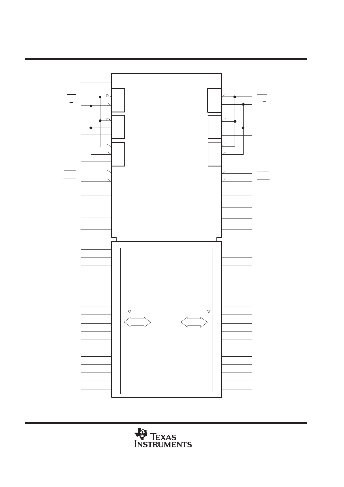
logic symbol
†
ENABLE
&
0
D2
A0
D1
A1
E2
A2
E1
A3
G3
A4
G1
A5
F1
A6
H1
A7
J1
A8
B1
D11
B2
E10
B3
E11
B4
G9
B5
G11
B6
F10
B7
H11
B8
J11
Data
1
K1
A9
L1
A10
K2
A11
L2
A12
L3
A13
L4
A14
J5
A15
L5
A16
17
K6
A17
B9
K11
B10
K10
B11
L11
B12
L10
B13
L9
B14
L8
B15
L6
B16
L7
B17
J7
17
RSTA
PENA
PROGRAM ENABLE
A1
RESET FIFOA–B
B3
A4
WENA
2
&
READ
FIFOB–A
OE1
&
ENABLE
&
WRITE
FIFOA–B
W/R
A
A3
CLOCK A
C5
CLKA
B5
RENA
CSA
A2
READ
ENABLE
FIFOA–B
&
WRITE
ENABLE
FIFOB–A
&
OE2
INPUT-READY
B1
IRA
OUTPUT-READY
A5
ORA
HALF-FULL
C2
HFA
ALMOST-FULL/EMPTY
B2
AF/AEA
FIFOA–B
PORT A
PORT A
FIFOA–B
B0
D10
0
CLKB
B6
CLOCK B
WENB
A8
RENB
B7
A10
B9
RESET FIFOB–A
B10
PROGRAM ENABLE
IRB
B11
INPUT-READY
ORB
A7
OUTPUT-READY
HFB
C10
HALF-FULL
AF/AEB
A11
ALMOST-FULL/EMPTY
FIFOB–A
FIFOB–A
PORT B
PORT B
FIFOB–A
RSTB
PENB
CSB
W/RB
A9
Φ
FIFO 512 × 18 × 2
SN54ABT7819
FIFOA–B
Data
†
This symbol is in accordance with ANSI/IEEE Std 91-1984 and IEC Publication 617-12.
Pin numbers shown are for the GB package.
SN54ABT7819
512 × 18 × 2
CLOCKED BIDIRECTIONAL FIRST-IN, FIRST-OUT MEMORY
SGBS305D – AUGUST 1994 – REVISED APRIL 1998
5
POST OFFICE BOX 655303 • DALLAS, TEXAS 75265
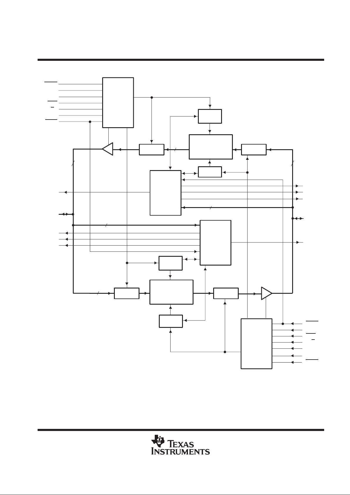
functional block diagram
A0–A17
HFA
ORA
AF/AEA
IRA
RSTA
CLKA
W/R
A
CSA
WENA
18
8
AF/AEB
IRB
WENB
W/R
B
CSB
CLKB
RSTB
B0–B17
18
18
8
Flag
Logic
FIFOB–A
Write
Pointer
Read
Pointer
Register
Port-A
Control
Logic
Register
HFB
18
512 × 18
Dual-Port SRAM
FIFOB–A
Port-B
Control
Logic
Read
Pointer
Write
Pointer
Register Register
512 × 18
Dual-Port SRAM
FIFOA–B
Flag
Logic
FIFOA–B
RENA
ORB
RENB
PENA
PENB
SN54ABT7819
512 × 18 × 2
CLOCKED BIDIRECTIONAL FIRST-IN, FIRST-OUT MEMORY
SGBS305D – AUGUST 1994 – REVISED APRIL 1998
6
POST OFFICE BOX 655303 • DALLAS, TEXAS 75265
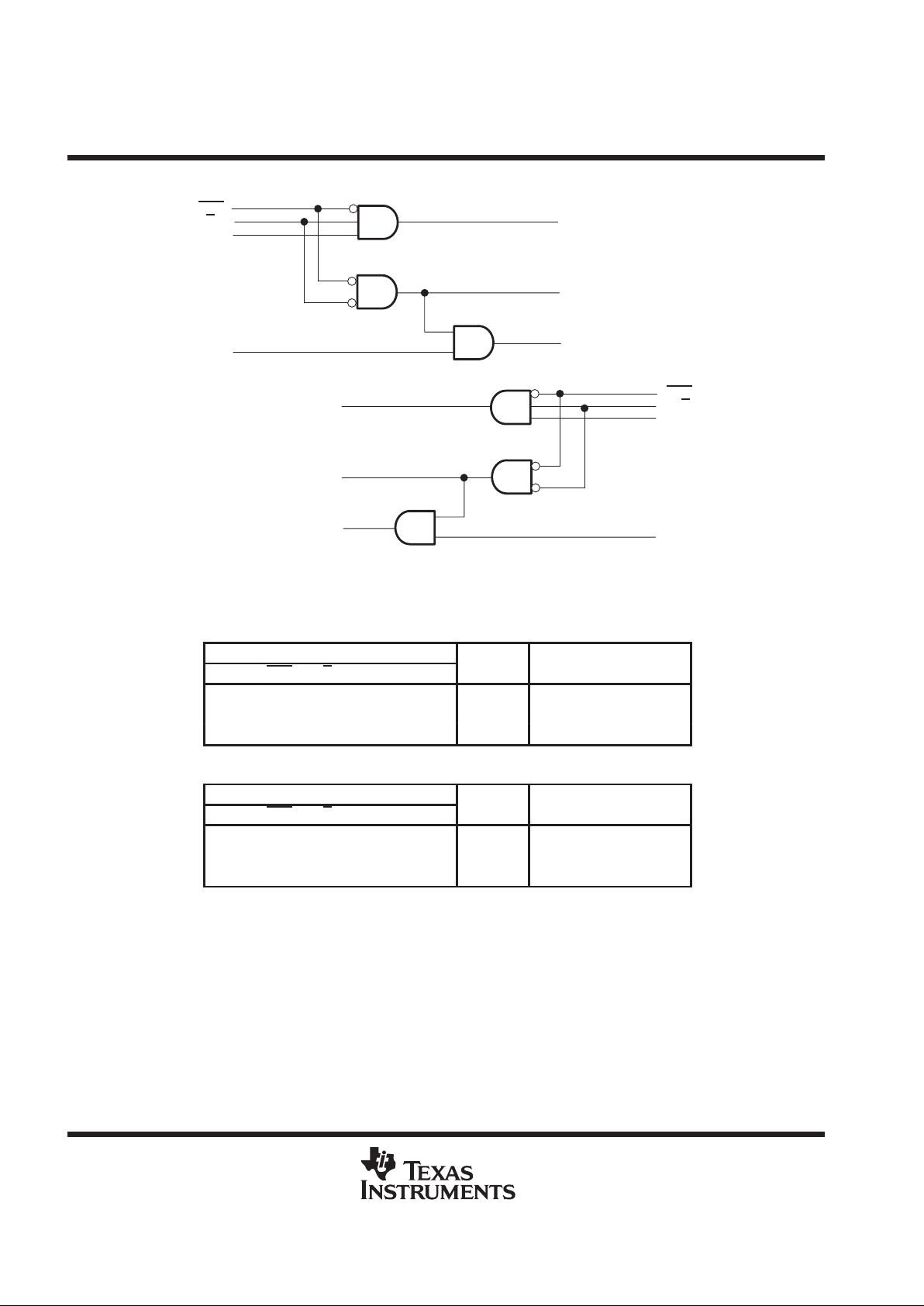
enable logic diagram (positive logic)
CSA
W/RA
WENA
RENA
WEN FIFOA–B
Output Enable (A0–A17)
REN FIFOB–A
CSB
W/RB
WENB
RENB
WEN FIFOB–A
Output Enable (B0–B17)
REN FIFOA–B
Function Tables
A PORT
SELECT INPUTS
CLKA CSA W/RA WENA RENA
A0–A17
OPERATION
X H X X X High Z None
↑ L H H X High Z Write A0–A17 to FIFOA–B
↑ L L X H Active Read FIFOB–A to A0–A17
B PORT
SELECT INPUTS
CLKB CSB W/RB WENB RENB
B0–B17
OPERATION
X H X X X High Z None
↑ L H H X High Z Write B0–B17 to FIFOB–A
↑ L L X H Active Read FIFOA–B to B0–B17
 Loading...