

SN54ABT533, SN74ABT533
OCTAL TRANSPARENT D-TYPE LATCHES
WITH 3-STATE OUTPUTS
SCBS186A – FEBRUARY 1991 – REVISED JULY 1994
• State-of-the-Art
EPIC-ΙΙB
BiCMOS Design
Significantly Reduces Power Dissipation
• Latch-Up Performance Exceeds 500 mA
Per JEDEC Standard JESD-17
• Typical V
(Output Ground Bounce)
OLP
< 1 V at VCC = 5 V, TA = 25°C
• High-Drive Outputs (–32-mA I
OH
,
64-mA IOL)
• Package Options Include Plastic
Small-Outline (DW) and Shrink
Small-Outline (DB) Packages, Ceramic
Chip Carriers (FK), and Plastic (N) and
Ceramic (J) DIPs
description
The ′ABT533 are 8-bit transparent D-type latches
with 3-state outputs designed specifically for
driving highly capacitive or relatively lowimpedance loads. They are particularly suitable
for implementing buffer registers, I/O ports,
bidirectional bus drivers, and working registers.
When the latch-enable (LE) input is high, the
Q
outputs follow the complements of the data
(D) inputs. When LE is taken low, the Q outputs
are latched at the inverse of the levels set up at the
D inputs. The ′ABT533 provides inverted data at
its outputs.
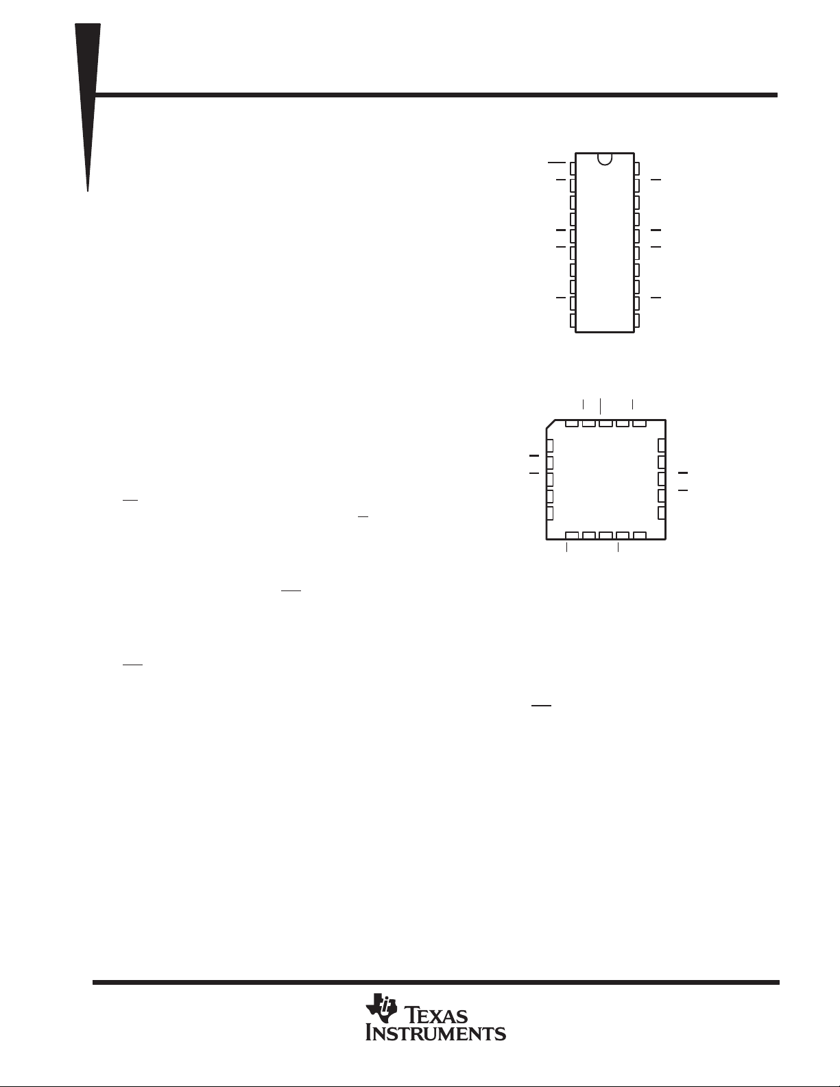
SN54ABT533 ...J PACKAGE
SN74ABT533 . . . DB, DW, OR N P ACKAGE
SN54ABT533 . . . FK PACKAGE
2D
2Q
3Q
3D
4D
(TOP VIEW)
OE
1Q
1D
2D
2Q
3Q
3D
4D
4Q
GND
(TOP VIEW)
1D1QOE
3212019
4
5
6
7
8
9
1
20
2
19
3
18
4
17
5
16
6
15
7
14
8
13
9
12
10
11
V
10 11 12 13
LE
4Q
GND
CC
5Q
V
8Q
8D
7D
7Q
6Q
6D
5D
5Q
LE
8Q
18
17
16
15
14
5D
CC
8D
7D
7Q
6Q
6D
A buffered output-enable (OE
) input can be used to place the eight outputs in either a normal logic state (high
or low logic levels) or a high-impedance state. In the high-impedance state, the outputs neither load nor drive
the bus lines significantly . The high-impedance state and the increased drive provide the capability to drive bus
lines without need for interface or pullup components.
OE does not affect the internal operations of the latches. Previously stored data can be retained or new data
can be entered while the outputs are in the high-impedance state.
T o ensure the high-impedance state during power up or power down, OE should be tied to VCC through a pullup
resistor; the minimum value of the resistor is determined by the current-sinking capability of the driver.
The SN74ABT533 is available in TI’s shrink small-outline package (DB), which provides the same I/O pin count
and functionality of standard small-outline packages in less than half the printed-circuit-board area.
The SN54ABT533 is characterized for operation over the full military temperature range of –55°C to 125°C. The
SN74ABT533 is characterized for operation from –40°C to 85°C.
EPIC-ΙΙB is a trademark of Texas Instruments Incorporated.
UNLESS OTHERWISE NOTED this document contains PRODUCTION
DATA information current as of publication date. Products conform to
specifications per the terms of Texas Instruments standard warranty.
Production processing does not necessarily include testing of all
parameters.
Copyright 1994, Texas Instruments Incorporated
POST OFFICE BOX 655303 • DALLAS, TEXAS 75265
2–1
SN54ABT533, SN74ABT533
OCTAL TRANSPARENT D-TYPE LATCHES
WITH 3-STATE OUTPUTS
SCBS186A – FEBRUAR Y 1991 – REVISED JULY 1994
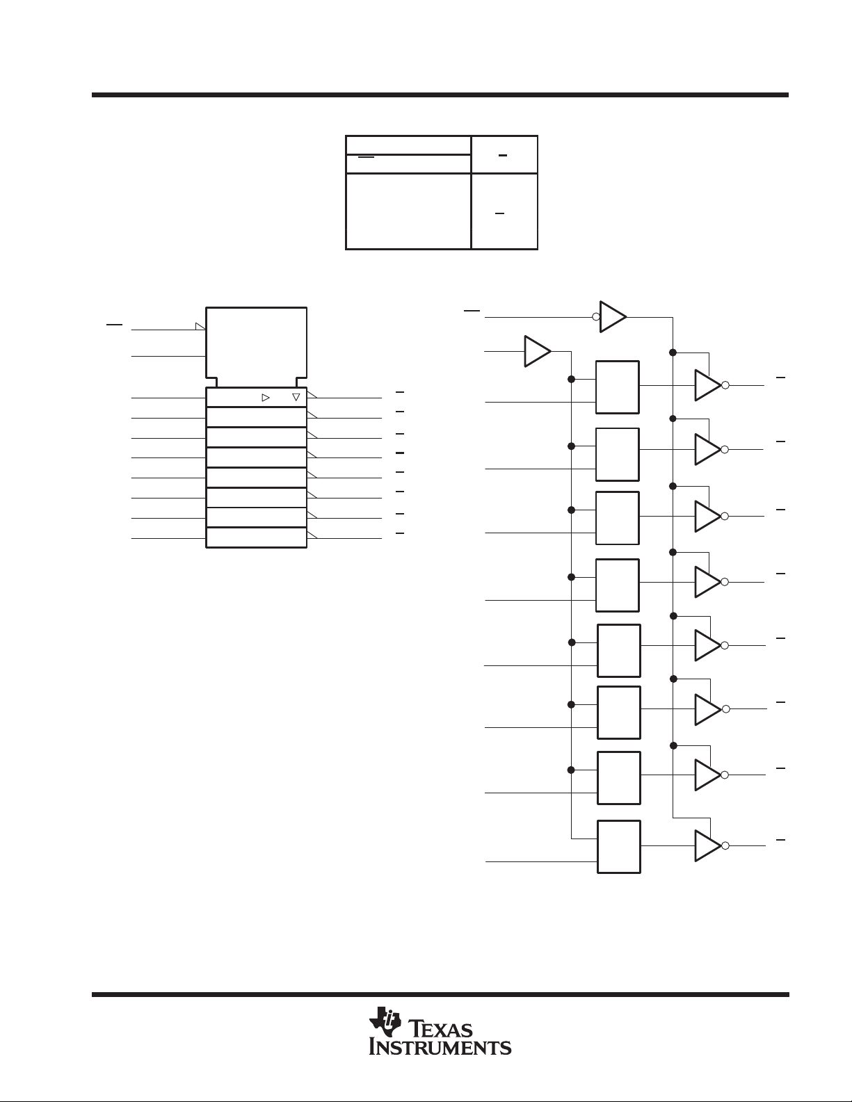
FUNCTION TABLE
INPUTS
OE LE D
L H H L
L HL H
L LX Q
H X X Z
(each latch)
OUTPUT
Q
0
logic symbol
1
OE
11
LE
3
1D
4
2D
7
3D
8
4D
13
5D
14
6D
17
7D
18
8D
†
This symbol is in accordance with ANSI/IEEE Std 91-1984
and IEC Publication 617-12.
†
EN
C1
1D
1
12
15
16
19
logic diagram (positive logic)
1
OE
11
LE
12
2
1Q
5
2Q
6
3Q
9
4Q
5Q
2
1Q
5
2Q
6
3Q
9
4Q
5Q
6Q
7Q
8Q
1D
2D
3D
4D
5D
3
4
7
8
13
C1
1D
C1
1D
C1
1D
C1
1D
C1
1D
2–2
14
6D
17
7D
18
8D
POST OFFICE BOX 655303 • DALLAS, TEXAS 75265
C1
1D
C1
1D
C1
1D
15
16
19
6Q
7Q
8Q
SN54ABT533, SN74ABT533
UNIT
OCTAL TRANSPARENT D-TYPE LATCHES
WITH 3-STATE OUTPUTS
SCBS186A – FEBRUARY 1991 – REVISED JULY 1994
absolute maximum ratings over operating free-air temperature range (unless otherwise noted)
Supply voltage range, V
CC
Input voltage range, VI (see Note 1) –0.5 V to 7 V. . . . . . . . . . . . . . . . . . . . . . . . . . . . . . . . . . . . . . . . . . . . . . . . . . .
Voltage range applied to any output in the high state or power-off state, V
O
Current into any output in the low state, IO: SN54ABT533 96 mA. . . . . . . . . . . . . . . . . . . . . . . . . . . . . . . . . . . .
SN74ABT533 128 mA. . . . . . . . . . . . . . . . . . . . . . . . . . . . . . . . . . . .
Input clamp current, I
Output clamp current, I
(V
< 0) –18 mA. . . . . . . . . . . . . . . . . . . . . . . . . . . . . . . . . . . . . . . . . . . . . . . . . . . . . . . . . . . .
IK
I
(V
OK
< 0) –50 mA. . . . . . . . . . . . . . . . . . . . . . . . . . . . . . . . . . . . . . . . . . . . . . . . . . . . . . . .
O
Maximum power dissipation at TA = 55°C (in still air) (see Note 2):DB package 0.6 W. . . . . . . . . . . . . . . . . . . .
DW package 1.6 W. . . . . . . . . . . . . . . . . . .
N package 1.3 W. . . . . . . . . . . . . . . . . . . . .
Storage temperature range –65°C to 150°C. . . . . . . . . . . . . . . . . . . . . . . . . . . . . . . . . . . . . . . . . . . . . . . . . . . . . . . .
†
Stresses beyond those listed under “absolute maximum ratings” may cause permanent damage to the device. These are stress ratings only, and
functional operation of the device at these or any other conditions beyond those indicated under “recommended operating conditions” is not
implied. Exposure to absolute-maximum-rated conditions for extended periods may affect device reliability.
NOTES: 1. The input and output negative-voltage ratings may be exceeded if the input and output clamp-current ratings are observed.
2. The maximum package power dissipation is calculated using a junction temperature of 150°C and a board trace length of 750 mils,
except for the N package, which has a trace length of zero. For more information, refer to the
application note in the 1994
ABT Advanced BiCMOS Technology Data Book
, literature number SCBD002B.
Package Thermal Considerations
–0.5 V to 7 V. . . . . . . . . . . . . . . . . . . . . . . . . . . . . . . . . . . . . . . . . . . . . . . . . . . . . . . . . .
–0.5 V to 5.5 V. . . . . . . . . . . . . . .
recommended operating conditions (see Note 3)
SN54ABT533 SN74ABT533
MIN MAX MIN MAX
V
CC
V
IH
V
IL
V
I
I
OH
I
OL
∆t/∆v Input transition rise or fall rate 10 10 ns/V
T
A
NOTE 3: Unused or floating inputs must be held high or low.
Supply voltage 4.5 5.5 4.5 5.5 V
High-level input voltage 2 2 V
Low-level input voltage 0.8 0.8 V
Input voltage 0 V
High-level output current –24 –32 mA
Low-level output current 48 64 mA
Operating free-air temperature –55 125 –40 85 °C
CC
0 V
CC
V
†
PRODUCT PREVIEW information concerns products in the formative or
design phase of development. Characteristic data and other
specifications are design goals. Texas Instruments reserves the right to
change or discontinue these products without notice.
POST OFFICE BOX 655303 • DALLAS, TEXAS 75265
2–3
 Loading...