

Texas Instruments SN74ABT273DBLE, SN74ABT273DBR, SN74ABT273DW, SN74ABT273DWR, SN74ABT273N Datasheet
...
OUTPUT
SN54ABT273, SN74ABT273
OCTAL EDGE-TRIGGERED D-TYPE FLIP-FLOPS
WITH CLEAR
SCBS185B – FEBRUARY 1991 – REVISED JANUARY 1997
D
State-of-the-Art
EPIC-ΙΙB
BiCMOS Design
Significantly Reduces Power Dissipation
D
Latch-Up Performance Exceeds 500 mA Per
JEDEC Standard JESD-17
D
T ypical V
(Output Ground Bounce) < 1 V
OLP
at VCC = 5 V, TA = 25°C
D
High-Drive Outputs (–32-mA IOH, 64-mA IOL)
D
Package Options Include Plastic
Small-Outline (DW), Shrink Small-Outline
(DB), and Thin Shrink Small-Outline (PW)
Packages, Ceramic Chip Carriers (FK),
Plastic (N) and Ceramic (J) DIPs, and
Ceramic Flat (W) Package
description
The ’ABT273 are 8-bit positive-edge-triggered
D-type flip-flops with a direct clear (CLR
They are particularly suitable for implementing
buffer and storage registers, shift registers, and
pattern generators.
Information at the data (D) inputs meeting the
setup time requirements is transferred to the
Q outputs on the positive-going edge of the clock
pulse. Clock triggering occurs at a particular
voltage level and is not directly related to the
transition time of the positive-going pulse. When
the clock (CLK) input is at either the high or low
level, the D input signal has no effect at the output.
) input.
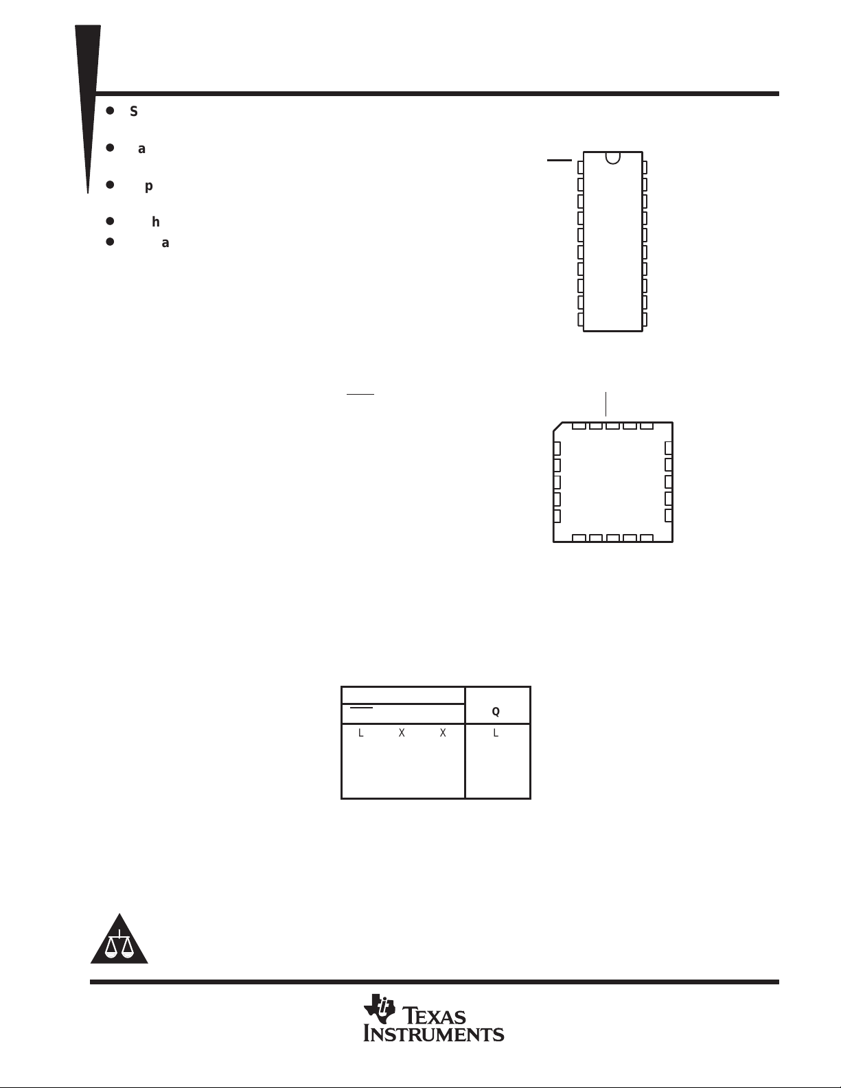
SN54ABT273 ...J OR W PACKAGE
SN74ABT273 . . . DB, DW, N, OR PW PACKAGE
SN54ABT273 . . . FK PACKAGE
2D
2Q
3Q
3D
4D
CLR
1Q
1D
2D
2Q
3Q
3D
4D
4Q
GND
3 2 1 20 19
4
5
6
7
8
9 10 11 12 13
(TOP VIEW)
20
1
19
2
18
3
17
4
16
5
15
6
14
7
13
8
12
9
11
10
(TOP VIEW)
1D1QCLR
4Q
GND
V
CLK
CC
5Q
V
CC
8Q
8D
7D
7Q
6Q
6D
5D
5Q
CLK
8Q
18
17
16
15
14
5D
8D
7D
7Q
6Q
6D
The SN54ABT273 is characterized for operation over the full military temperature range of –55°C to 125°C. The
SN74ABT273 is characterized for operation from –40°C to 85°C.
FUNCTION TABLE
(each flip-flop)
CLR
L X X L
H ↑ HH
H ↑ LL
H H or L X Q
Please be aware that an important notice concerning availability, standard warranty, and use in critical applications of
Texas Instruments semiconductor products and disclaimers thereto appears at the end of this data sheet.
EPIC-ΙΙB is a trademark of Texas Instruments Incorporated.
PRODUCTION DATA information is current as of publication date.
Products conform to specifications per the terms of Texas Instruments
standard warranty. Production processing does not necessarily include
testing of all parameters.
INPUTS
CLK D
OUTPUT
Q
0
Copyright 1997, Texas Instruments Incorporated
POST OFFICE BOX 655303 • DALLAS, TEXAS 75265
1
SN54ABT273, SN74ABT273
OCTAL EDGE-TRIGGERED D-TYPE FLIP-FLOPS
WITH CLEAR
SCBS185B – FEBRUARY 1991 – REVISED JANUARY 1997
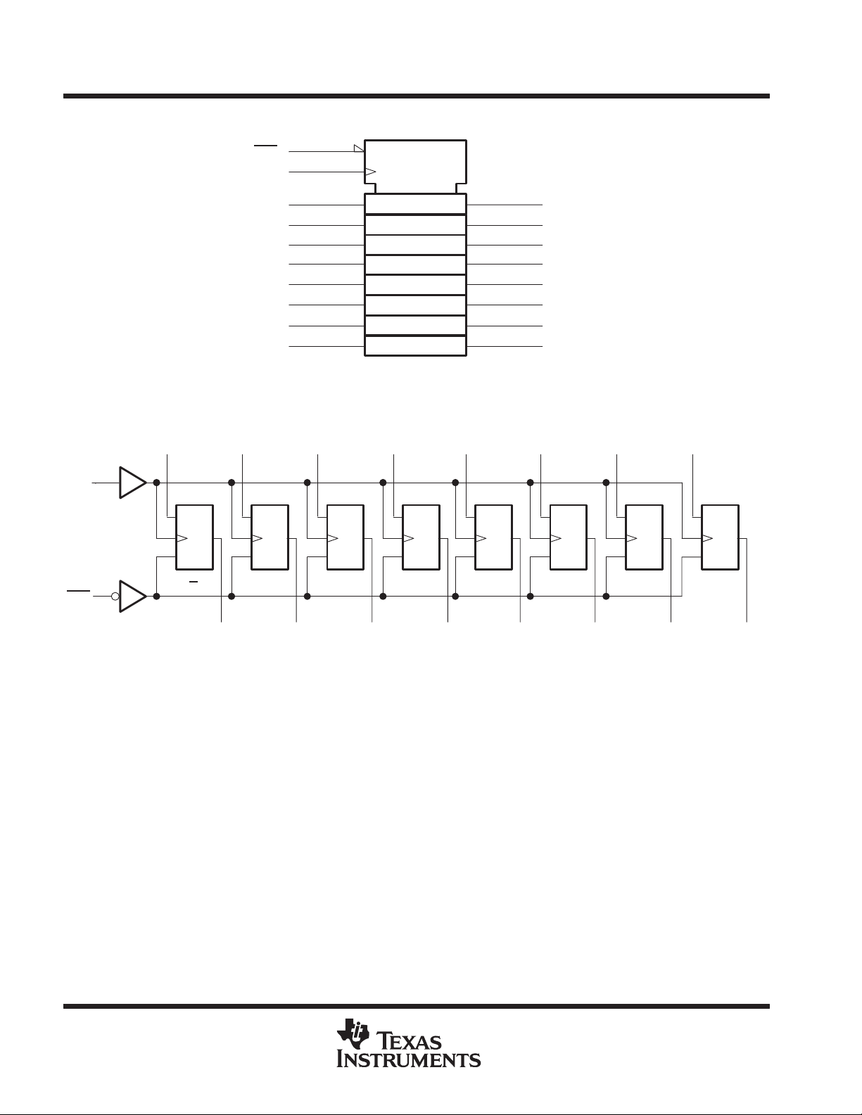
logic symbol
†
This symbol is in accordance with ANSI/IEEE Std 91-1984 and IEC Publication 617-12.
†
CLR
CLK
1D
2D
3D
4D
5D
6D
7D
8D
1
11
3
4
7
8
13
14
17
18
R
C1
1D
logic diagram (positive logic)
CLK
1D
11
3
CLK(I)
1D
C1
R
2D
4
1D
C1
R
3D
4D
7
1D
C1
R
8
1D
R
5D
C1
13
1D
R
C1
12
15
16
19
2
1Q
5
2Q
6
3Q
9
4Q
5Q
6Q
7Q
8Q
6D
14
1D
C1
R
7D
17
1D
R
C1
8D
18
1D
C1
R
CLR
1
R
2
1Q
2Q
5
3Q
6
4Q
9
5Q
12
6Q
15
7Q
16
8Q
absolute maximum ratings over operating free-air temperature range (unless otherwise noted)
Supply voltage range, VCC –0.5 V to 7 V. . . . . . . . . . . . . . . . . . . . . . . . . . . . . . . . . . . . . . . . . . . . . . . . . . . . . . . . . .
Input voltage range, VI (see Note 1) –0.5 V to 7 V. . . . . . . . . . . . . . . . . . . . . . . . . . . . . . . . . . . . . . . . . . . . . . . . . .
Voltage range applied to any output in the high or power-off state, V
Current into any output in the low state, IO: SN54ABT273 96 mA. . . . . . . . . . . . . . . . . . . . . . . . . . . . . . . . . . . .
SN74ABT273 128 mA. . . . . . . . . . . . . . . . . . . . . . . . . . . . . . . . . . .
Input clamp current, IIK (VI < 0) –18 mA. . . . . . . . . . . . . . . . . . . . . . . . . . . . . . . . . . . . . . . . . . . . . . . . . . . . . . . . . . .
Output clamp current, IOK (VO < 0) –50 mA. . . . . . . . . . . . . . . . . . . . . . . . . . . . . . . . . . . . . . . . . . . . . . . . . . . . . . . .
Package thermal impedance, θ
(see Note 2): DB package 115°C/W. . . . . . . . . . . . . . . . . . . . . . . . . . . . . . . .
JA
DW package 97°C/W. . . . . . . . . . . . . . . . . . . . . . . . . . . . . . . . .
N package 67°C/W. . . . . . . . . . . . . . . . . . . . . . . . . . . . . . . . . . .
PW package 128°C/W. . . . . . . . . . . . . . . . . . . . . . . . . . . . . . . .
Storage temperature range, T
‡
Stresses beyond those listed under “absolute maximum ratings” may cause permanent damage to the device. These are stress ratings only, and
functional operation of the device at these or any other conditions beyond those indicated under “recommended operating conditions” is not
implied. Exposure to absolute-maximum-rated conditions for extended periods may affect device reliability.
NOTES: 1. The input and output negative-voltage ratings may be exceeded if the input and output clamp-current ratings are observed.
2. The package thermal impedance is calculated in accordance with EIA/JEDEC Std JESD51, except for through-hole packages,
which use a trace length of zero.
–65°C to 150°C. . . . . . . . . . . . . . . . . . . . . . . . . . . . . . . . . . . . . . . . . . . . . . . . . . .
stg
–0.5 V to 5.5 V. . . . . . . . . . . . . . . . . . .
O
19
‡
2
POST OFFICE BOX 655303 • DALLAS, TEXAS 75265
 Loading...