

Texas Instruments SNJ54ABT18646HV Datasheet
SN54ABT18646
SCAN TEST DEVICE WITH
18-BIT TRANSCEIVERS AND REGISTERS
SGBS306 – AUGUST 1992 – REVISED AUGUST 1994
Copyright 1994, Texas Instruments Incorporated
4–1
POST OFFICE BOX 655303 • DALLAS, TEXAS 75265
• Members of the Texas Instruments
SCOPE
Family of Testability Products
• Members of the Texas Instruments
Widebus
Family
• Compatible With the IEEE Standard
1149.1-1990 (JTAG) Test Access Port and
Boundary-Scan Architecture
• Includes D-Type Flip-Flops and Control
Circuitry to Provide Multiplexed
Transmission of Stored and Real-Time Data
• Two Boundary-Scan Cells per I/O for
Greater Flexibility
• State-of-the-Art
EPIC-ΙΙB
BiCMOS Design
Significantly Reduces Power Dissipation
•
SCOPE
Instruction Set
– IEEE Standard 1149.1-1990 Required
Instructions, Optional INTEST, CLAMP
and HIGHZ
– Parallel-Signature Analysis at Inputs With
Masking Option
– Pseudo-Random Pattern Generation
From Outputs
– Sample Inputs/Toggle Outputs
– Binary Count From Outputs
– Device Identification
– Even-Parity Opcodes
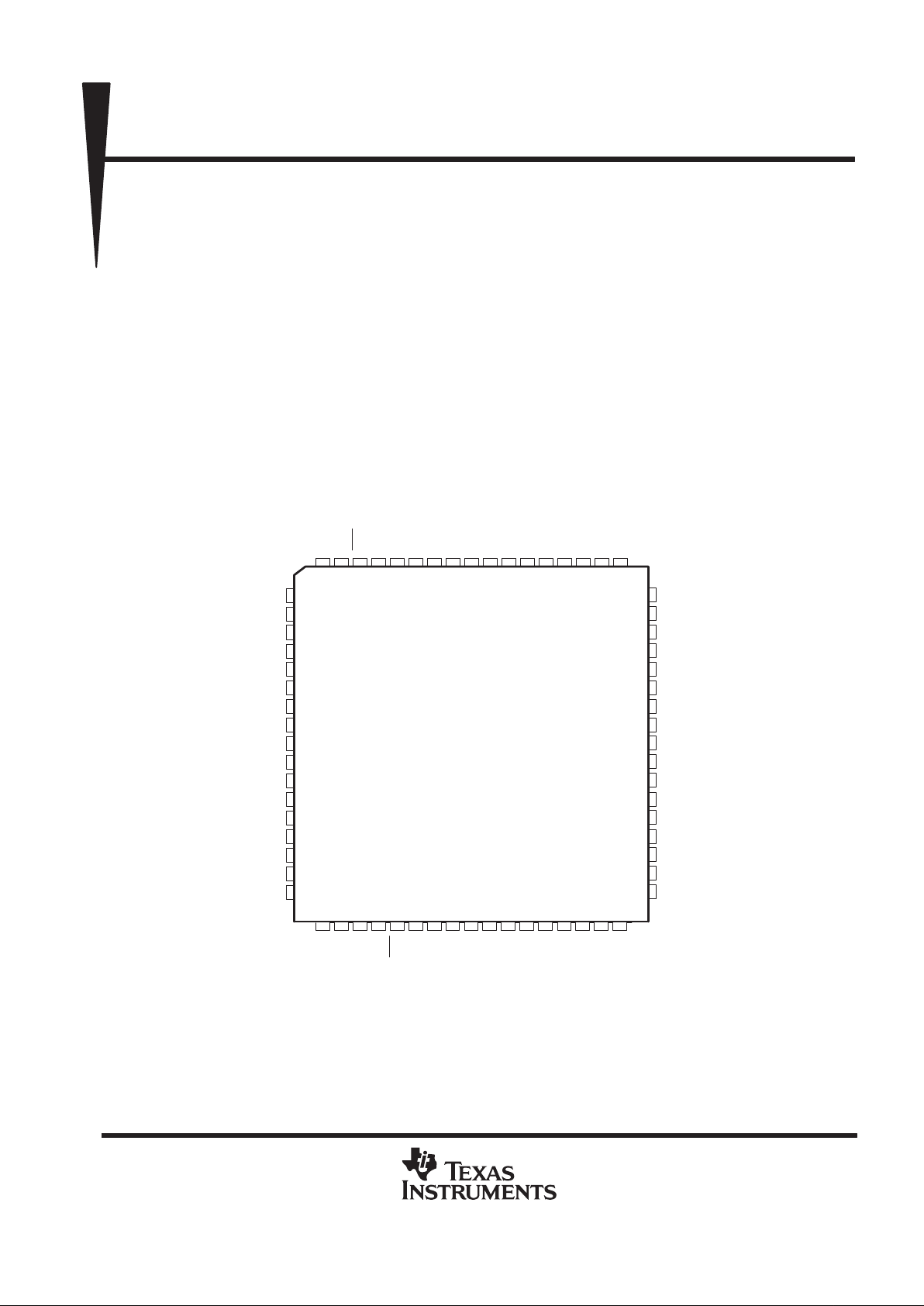
• Packaged in 68-Pin Ceramic Quad Flat
Package
1B4
1B5
1B6
GND
1B7
1B8
1B9
V
CC
NC
2B1
2B2
2B3
2B4
GND
2B5
2B6
2B7
1A3
1A4
1A5
GND
1A6
1A7
1A8
1A9
NC
V
CC
2A1
2A2
2A3
GND
2A4
2A5
2A6
VNCTMS
1CLKBA
1A2
1A1
1OE
GND
1SAB
1CLKAB
TDO
NC
TCK
2CLKBA
2SBA
2A9
GND
2OE
2SAB
2CLKAB
TDI
2A7
2A8
1SBA
1DIR
GND
2DIR
2B9
2B8
GND
1B1
1B2
1B3
28 29
60
59
58
57
56
55
54
53
52
51
50
49
48
47
46
45
44
30
10
11
12
13
14
15
16
17
18
19
20
21
22
23
24
25
26
31 32 33 34
87 65493168672
35 36 37 38 39
66 652764 63 62 61
40 41 42 43
HV PACKAGE
(TOP VIEW)
CC
V
CC
NC – No internal connection
SCOPE, Widebus, and EPIC-ΙΙB are trademarks of Texas Instruments Incorporated.
PRODUCTION DATA information is current as of publication date.
Products conform to specifications per the terms of Texas Instruments
standard warranty. Production processing does not necessarily include
testing of all parameters.
SN54ABT18646
SCAN TEST DEVICE WITH
18-BIT TRANSCEIVERS AND REGISTERS
SGBS306 – AUGUST 1992 – REVISED AUGUST 1994
4–2
POST OFFICE BOX 655303 • DALLAS, TEXAS 75265
description
The SN54ABT18646 scan test device with 18-bit bus transceivers and registers is a member of the Texas
Instruments SCOPE testability integrated circuit family. This family of devices supports IEEE Standard
1149.1-1990 boundary scan to facilitate testing of complex circuit-board assemblies. Scan access to the test
circuitry is accomplished via the 4-wire test access port (TAP) interface.
In the normal mode, the SN54ABT18646 is an 18-bit bus transceiver and register that allows for multiplexed
transmission of data directly from the input bus or from the internal registers. It can be used either as two 9-bit
transceivers or one 18-bit transceiver. The test circuitry can be activated by the TAP to take snapshot samples
of the data appearing at the device pins or to perform a self test on the boundary-test cells. Activating the T AP
in the normal mode does not affect the functional operation of the SCOPE bus transceivers and registers.
Transceiver function is controlled by output-enable (OE
) and direction (DIR) inputs. When OE is low, the
transceiver is active and operates in the A-to-B direction when DIR is high or in the B-to-A direction when DIR
is low. When OE
is high, both the A and B outputs are in the high-impedance state, effectively isolating both
buses.
Data flow is controlled by clock (CLKAB and CLKBA) and select (SAB and SBA) inputs. Data on the A bus is
clocked into the associated registers on the low-to-high transition of CLKAB. When SAB is low, real-time A data
is selected for presentation to the B bus (transparent mode). When SAB is high, stored A data is selected for
presentation to the B bus (registered mode). The function of the CLKBA and SBA inputs mirrors that of CLKAB
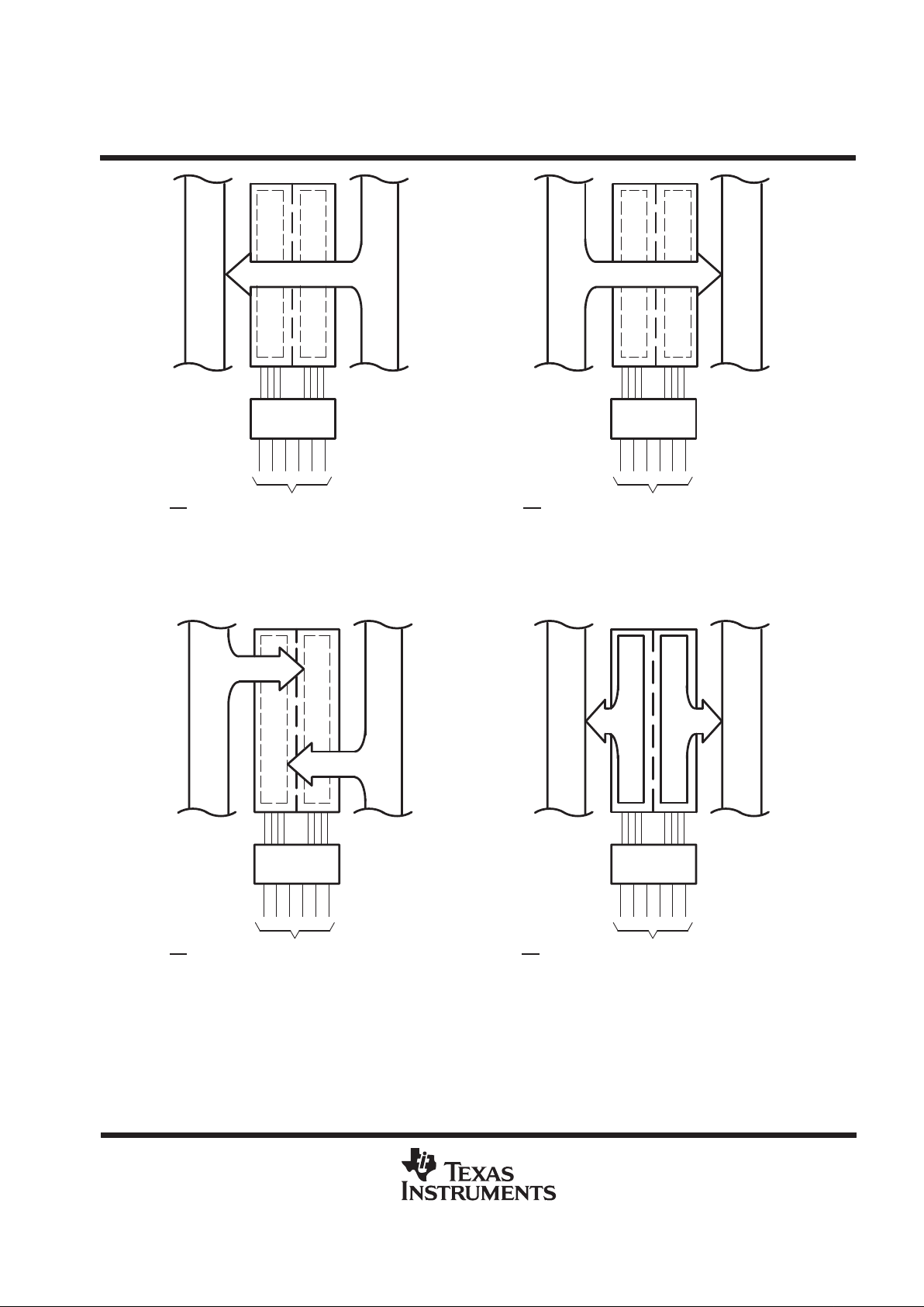
and SAB, respectively. Figure 1 illustrates the four fundamental bus-management functions that can be
performed with the
SN54
ABT18646.
In the test mode, the normal operation of the SCOPE bus transceivers and registers is inhibited, and the test
circuitry is enabled to observe and control the I/O boundary of the device. When enabled, the test circuitry can
perform boundary-scan test operations according to the protocol described in IEEE Standard 1149.1-1990.
Four dedicated test pins observe and control the operation of the test circuitry: test data input (TDI), test data
output (TDO), test mode select (TMS), and test clock (TCK). Additionally , the test circuitry performs other testing
functions such as parallel-signature analysis (PSA) on data inputs and pseudo-random pattern generation
(PRPG) from data outputs. All testing and scan operations are synchronized to the TAP interface.
Additional flexibility is provided in the test mode through the use of two boundary scan cells (BSCs) for each
I/O pin. This allows independent test data to be captured and forced at either bus (A or B). A PSA/COUNT
instruction also is included to ease the testing of memories and other circuits where a binary count addressing
scheme is useful.
The SN54ABT18646 is characterized over the full military temperature range of –55°C to 125°C.
FUNCTION TABLE
(normal mode, each 9-bit section)
INPUTS
DATA I/O
OE DIR CLKAB CLKBA SAB SBA A1 THRU A9 B1 THRU B9
OPERATION OR FUNCTION
X X ↑ X X X Input Unspecified
†
Store A, B unspecified
†
X XX ↑X X Unspecified
†
Input Store B, A unspecified
†
H X ↑ ↑ X X Input Input Store A and B data
H X L L X X Input disabled Input disabled Isolation, hold storage
L L X X X L Output Input Real-time B data to A bus
L L X X X H Output Input disabled Stored B data to A bus
L H X X L X Input Output Real-time A data to B bus
L H X X H X Input disabled Output Stored A data to B bus
†
The data output functions can be enabled or disabled by various signals at the OE and DIR inputs. Data input functions are always enabled; i.e.,
data at the bus pins is stored on every low-to-high transition of the clock inputs.
SN54ABT18646
SCAN TEST DEVICE WITH
18-BIT TRANSCEIVERS AND REGISTERS
SGBS306 – AUGUST 1992 – REVISED AUGUST 1994
4–3
POST OFFICE BOX 655303 • DALLAS, TEXAS 75265
L
DIRLCLKABXCLKBAXSABXSBA
L
REAL-TIME TRANSFER
BUS B TO BUS A
L
DIRHCLKABXCLKBAXSABLSBA
X
REAL-TIME TRANSFER
BUS A TO BUS B
X
DIRXCLKAB CLKBAXSABXSBA
X
STORAGE FROM
A, B, OR A AND B
L
DIRLCLKABXCLKBAXSABXSBA
H
TRANSFER STORED DATA
TO A AND/OR B
X
H
X
X
XX
X
X
X
LH X XHX
↑
↑
↑↑
BUS B
BUS A
BUS B
BUS A
BUS B
BUS A
BUS B
BUS A
OE
OE
OEOE
Figure 1. Bus-Management Functions
SN54ABT18646
SCAN TEST DEVICE WITH
18-BIT TRANSCEIVERS AND REGISTERS
SGBS306 – AUGUST 1992 – REVISED AUGUST 1994
4–4
POST OFFICE BOX 655303 • DALLAS, TEXAS 75265
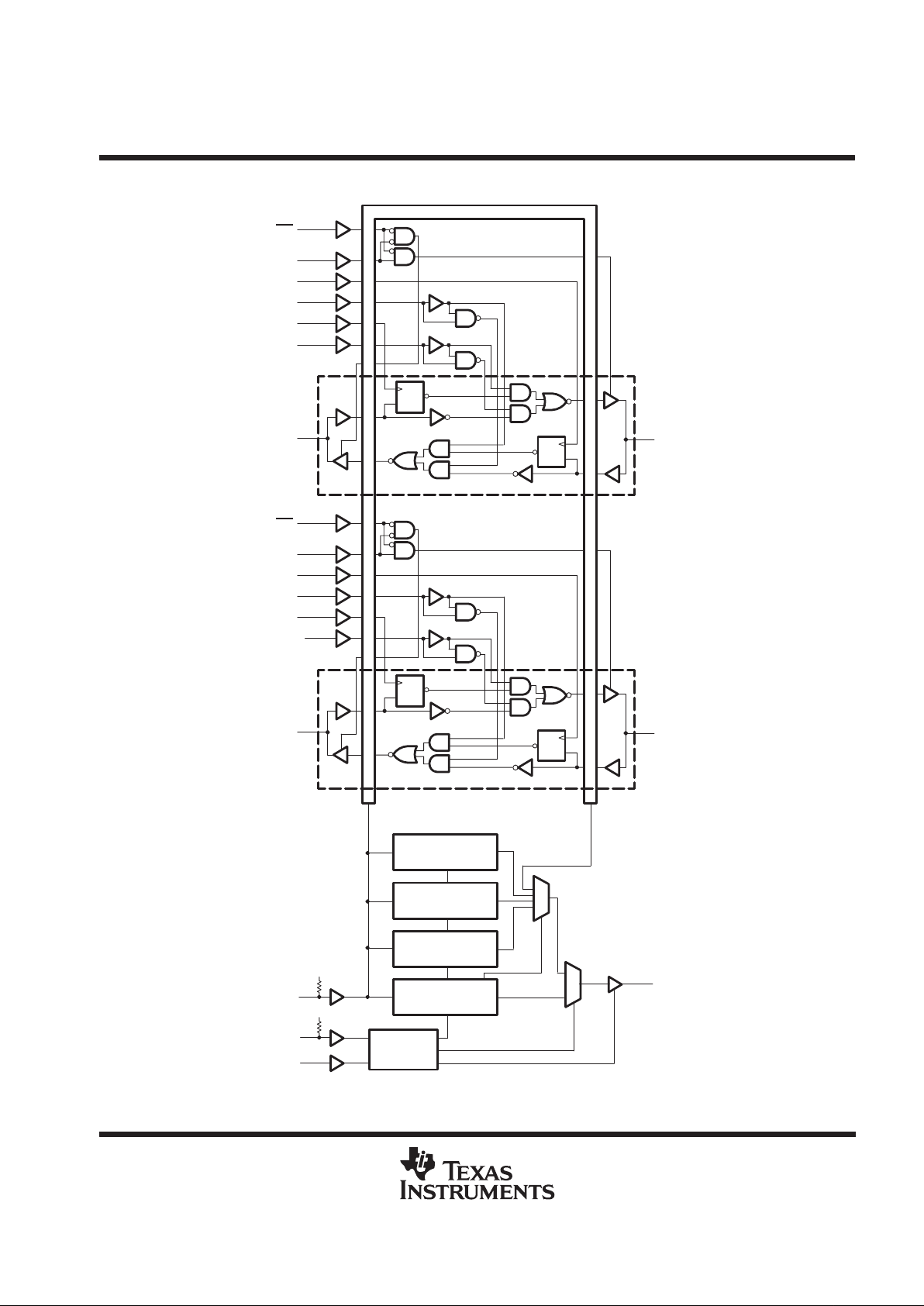
functional block diagram
Boundary-Scan Register
One of Nine Channels
1OE
1DIR
1CLKBA
1SBA
1CLKAB
1SAB
1A1
1B1
1D
C1
1D
C1
One of Nine Channels
2OE
2DIR
2CLKBA
2SBA
2CLKAB
2SAB
2A1
2B1
1D
C1
1D
C1
Boundary-Control
Register
Instruction
Register
TDI
TMS
TCK
TDO
TAP
Controller
V
CC
V
CC
Bypass Register
Identification
Register
7
65
67
66
4
5
8
31
41
38
39
33
32
20
34
68
37
63
51
3
SN54ABT18646
SCAN TEST DEVICE WITH
18-BIT TRANSCEIVERS AND REGISTERS
SGBS306 – AUGUST 1992 – REVISED AUGUST 1994
4–5
POST OFFICE BOX 655303 • DALLAS, TEXAS 75265
Terminal Functions
TERMINAL NAME DESCRIPTION
1A1–1A9,
2A1–2A9
Normal-function A-bus I/O ports. See function table for normal-mode logic.
1B1–1B9,
2B1–2B9
Normal-function B-bus I/O ports. See function table for normal-mode logic.
1CLKAB, 1CLKBA,
2CLKAB, 2CLKBA
Normal-function clock inputs. See function table for normal-mode logic.
1DIR, 2DIR Normal-function direction controls. See function table for normal-mode logic.
GND Ground
1OE, 2OE Normal-function output enables. See function table for normal-mode logic.
1SAB, 1SBA,
2SAB, 2SBA
Normal-function select controls. See function table for normal-mode logic.
TCK
T est clock. One of four terminals required by IEEE Standard 1 149.1-1990. Test operations of the device are synchronous
to TCK. Data is captured on the rising edge of TCK and outputs change on the falling edge of TCK.
TDI
Test data input. One of four terminals required by IEEE Standard 1149.1-1990. TDI is the serial input for shifting data
through the instruction register or selected data register. An internal pullup forces TDI to a high level if left unconnected.
TDO
T est data output. One of four terminals required by IEEE Standard 1 149.1-1990. TDO is the serial output for shifting data
through the instruction register or selected data register.
TMS
T est mode select. One of four terminals required by IEEE Standard 1 149.1-1990. TMS directs the device through its T AP
controller states. An internal pullup forces TMS to a high level if left unconnected.
V
CC
Supply voltage
SN54ABT18646
SCAN TEST DEVICE WITH
18-BIT TRANSCEIVERS AND REGISTERS
SGBS306 – AUGUST 1992 – REVISED AUGUST 1994
4–6
POST OFFICE BOX 655303 • DALLAS, TEXAS 75265
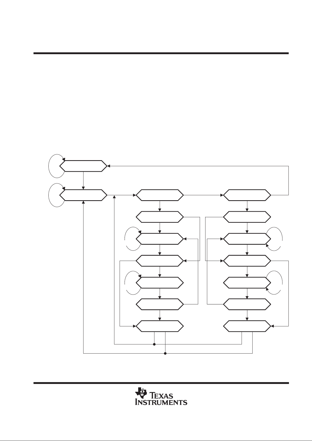
test architecture
Serial-test information is conveyed by means of a 4-wire test bus or TAP that conforms to IEEE Standard
1 149.1-1990. Test instructions, test data, and test control signals all are passed along this serial-test bus. The
T AP controller monitors two signals from the test bus, namely TCK and TMS. The TAP controller extracts the
synchronization (TCK) and state control (TMS) signals from the test bus and generate the appropriate on-chip
control signals for the test structures in the device. Figure 2 shows the TAP-controller state diagram.
The T AP controller is fully synchronous to the TCK signal. Input data is captured on the rising edge of TCK, and
output data changes on the falling edge of TCK. This scheme ensures that data to be captured is valid for fully
one-half of the TCK cycle.
The functional block diagram illustrates the IEEE Standard 1149.1-1990 4-wire test bus and boundary-scan
architecture and the relationship among the test bus, the TAP controller, and the test registers. As illustrated,
the device contains an 8-bit instruction register and four test data registers: an 88-bit boundary-scan register,
a 21-bit boundary-control register, a 1-bit bypass register, and a 32-bit device-identification register.
Test-Logic-Reset
Run-Test/Idle Select-DR-Scan
Capture-DR
Shift-DR
Exit1-DR
Pause-DR
Update-DR
TMS = L
TMS = L
TMS = H
TMS = L
TMS = H
TMS = H
TMS = LTMS = H
TMS = L
TMS = L
TMS = H
TMS = L
Exit2-DR
Select-IR-Scan
Capture-IR
Shift-IR
Exit1-IR
Pause-IR
Update-IR
TMS = L
TMS = L
TMS = H
TMS = L
TMS = H
TMS = H
TMS = LTMS = H
TMS = L
Exit2-IR
TMS = L
TMS = H TMS = H
TMS = H
TMS = L
TMS = H
TMS = L
TMS = HTMS = H
TMS = H
TMS = L
Figure 2. TAP-Controller State Diagram

SN54ABT18646
SCAN TEST DEVICE WITH
18-BIT TRANSCEIVERS AND REGISTERS
SGBS306 – AUGUST 1992 – REVISED AUGUST 1994
4–7
POST OFFICE BOX 655303 • DALLAS, TEXAS 75265
state diagram description
The T AP controller is a synchronous finite state machine that provides test control signals throughout the device.
The state diagram is illustrated in Figure 2 and is in accordance with IEEE Standard 1149.1-1990. The TAP
controller proceeds through its states based on the level of TMS at the rising edge of TCK.
As illustrated, the T AP controller consists of 16 states. There are six stable states (indicated by a looping arrow
in the state diagram) and ten unstable states. A stable state is defined as a state the T AP controller can retain
for consecutive TCK cycles. Any state that does not meet this criterion is an unstable state.
There are two main paths through the state diagram: one to access and control the selected data register and
one to access and control the instruction register. Only one register can be accessed at a time.
Test-Logic-Reset
The device powers up in the T est-Logic-Reset state. In the stable Test-Logic-Reset state, the test logic is reset
and is disabled so that the normal logic function of the device is performed. The instruction register is reset to
an opcode that selects the optional IDCODE instruction, if supported, or the BYP ASS instruction. Certain data
registers also can be reset to their power-up values.
The state machine is constructed such that the T AP controller returns to the Test-Logic-Reset state in no more
than five TCK cycles if TMS is left high. The TMS pin has an internal pullup resistor that forces it high if left
unconnected or if a board defect causes it to be open circuited.
For the SN54ABT18646, the instruction register is reset to the binary value 10000001, which selects the
IDCODE instruction. Bits 87– 84 in the boundary-scan register are reset to logic 0, ensuring that these cells,
which control A-port and B-port outputs, are set to benign values (i.e., if test mode were invoked, the outputs
would be at high impedance state). Reset values of other bits in the boundary-scan register should be
considered indeterminate. The boundary-control register is reset to the binary value 000000000000000000010,
which selects the PSA test operation with no input masking.
Run-T est/Idle
The T AP controller must pass through the Run-T est/Idle state (from T est-Logic-Reset) before executing any test
operations. The Run-Test/Idle state also can be entered following data-register or instruction-register scans.
Run-Test/Idle is a stable state in which the test logic can be actively running a test or can be idle.
The test operations selected by the boundary-control register are performed while the T AP controller is in the
Run-Test/Idle state.
Select-DR-Scan, Select-lR-Scan
No specific function is performed in the Select-DR-Scan and Select-lR-Scan states, and the T AP controller exits
either of these states on the next TCK cycle. These states allow the selection of either data-register scan or
instruction-register scan.
Capture-DR
When a data-register scan is selected, the TAP controller must pass through the Capture-DR state. In the
Capture-DR state, the selected data register can capture a data value as specified by the current instruction.
Such capture operations occur on the rising edge of TCK upon which the T AP controller exits the Capture-DR
state.
Shift-DR
Upon entry to the Shift-DR state, the data register is placed in the scan path between TDI and TDO and, on the
first falling edge of TCK, TDO goes from the high-impedance state to an active state. TDO enables to the logic
level present in the least significant bit of the selected data register.

SN54ABT18646
SCAN TEST DEVICE WITH
18-BIT TRANSCEIVERS AND REGISTERS
SGBS306 – AUGUST 1992 – REVISED AUGUST 1994
4–8
POST OFFICE BOX 655303 • DALLAS, TEXAS 75265
Shift-DR (continued)
While in the stable Shift-DR state, data is serially shifted through the selected data register on each TCK cycle.
The first shift occurs on the first rising edge of TCK after entry to the Shift-DR state (i.e., no shifting occurs during
the TCK cycle in which the T AP controller changes from Capture-DR to Shift-DR or from Exit2-DR to Shift-DR).
The last shift occurs on the rising edge of TCK upon which the TAP controller exits the Shift-DR state.
Exit1-DR, Exit2-DR
The Exit1-DR and Exit2-DR states are temporary states that end a data-register scan. It is possible to return
to the Shift-DR state from either Exit1-DR or Exit2-DR without recapturing the data register. On the first falling
edge of TCK after entry to Exit1-DR, TDO goes from the active state to the high-impedance state.
Pause-DR
No specific function is performed in the stable Pause-DR state, in which the TAP controller can remain
indefinitely . The Pause-DR state can suspend and resume data-register scan operations without loss of data.
Update-DR
If the current instruction calls for the selected data register to be updated with current data, such update occurs
on the falling edge of TCK following entry to the Update-DR state.
Capture-IR
When an instruction-register scan is selected, the T AP controller must pass through the Capture-IR state. In the
Capture-IR state, the instruction register captures its current status value. This capture operation occurs on the
rising edge of TCK upon which the T AP controller exits the Capture-IR state. For the SN54ABT18646, the status
value loaded in the Capture-IR state is the fixed binary value 10000001.
Shift-IR
Upon entry to the Shift-IR state, the instruction register is placed in the scan path between TDI and TDO and,
on the first falling edge of TCK, TDO goes from the high-impedance state to an active state. TDO enables to
the logic level present in the least significant bit of the instruction register.
While in the stable Shift-IR state, instruction data is serially shifted through the instruction register on each TCK
cycle. The first shift occurs on the first rising edge of TCK after entry to the Shift-IR state (i.e., no shifting occurs
during the TCK cycle in which the TAP controller changes from Capture-IR to Shift-IR or from Exit2-IR to
Shift-IR). The last shift occurs on the rising edge of TCK upon which the T AP controller exits the Shift-IR state.
Exit1-IR, Exit2-IR
The Exit1-IR and Exit2-IR states are temporary states that end an instruction-register scan. It is possible to
return to the Shift-IR state from either Exit1-IR or Exit2-IR without recapturing the instruction register. On the
first falling edge of TCK after entry to Exit1-IR, TDO goes from the active state to the high-impedance state.
Pause-IR
No specific function is performed in the stable Pause-IR state, in which the T AP controller can remain indefinitely.
The Pause-IR state can suspend and resume instruction-register scan operations without loss of data.
Update-IR
The current instruction is updated and takes effect on the falling edge of TCK following entry to the Update-IR
state.

SN54ABT18646
SCAN TEST DEVICE WITH
18-BIT TRANSCEIVERS AND REGISTERS
SGBS306 – AUGUST 1992 – REVISED AUGUST 1994
4–9
POST OFFICE BOX 655303 • DALLAS, TEXAS 75265
register overview
With the exception of the bypass and device-identification registers, any test register can be thought of as a
serial-shift register with a shadow latch on each bit. The bypass and device-identification registers differ in that
they contain only a shift register. During the appropriate capture state (Capture-IR for instruction register,
Capture-DR for data registers), the shift register can be parallel loaded from a source specified by the current
instruction. During the appropriate shift state (Shift-IR or Shift-DR), the contents of the shift register are shifted
out from TDO while new contents are shifted in at TDI. During the appropriate update state (Update-IR or
Update-DR), the shadow latches are updated from the shift register.
instruction register description
The instruction register (IR) is eight bits long and tells the device what instruction is to be executed. Information
contained in the instruction includes the mode of operation (either normal mode, in which the device performs
its normal logic function, or test mode, in which the normal logic function is inhibited or altered), the test operation
to be performed, which of the four data registers is to be selected for inclusion in the scan path during
data-register scans, and the source of data to be captured into the selected data register during Capture-DR.
T able 4 lists the instructions supported by the SN54ABT18646. The even-parity feature specified for SCOPE
devices is supported in this device. Bit 7 of the instruction opcode is the parity bit. Any instructions that are
defined for SCOPE devices but are not supported by this device default to BYPASS.
During Capture-IR, the IR captures the binary value 10000001. As an instruction is shifted in, this value will be
shifted out via TDO and can be inspected as verification that the IR is in the scan path. During Update-IR, the
value that has been shifted into the IR is loaded into shadow latches. At this time, the current instruction is
updated and any specified mode change takes effect. At power up or in the Test-Logic-Reset state, the IR is
reset to the binary value 10000001, which selects the IDCODE instruction. The IR order of scan is illustrated
in Figure 3.
Bit 6 Bit 5 Bit 4 Bit 3 Bit 2 Bit 1
TDOTDI
Bit 7
Parity
(MSB)
Bit 0
(LSB)
Figure 3. Instruction Register Order of Scan
 Loading...