

Texas Instruments JM38510-36101B2A, JM38510-36101BFA, JM38510-36101BEA, SN54173J, SN54LS173AJ Datasheet
...
SN54173, SN54LS173A, SN74173, SN74LS173A
4-BIT D-TYPE REGISTERS
WITH 3-STATE OUTPUTS
SDLS067A – OCTOBER 1976 – REVISED JUNE 1999
D
3-State Outputs Interface Directly With
System Bus
D
Gated Output-Control LInes for Enabling or
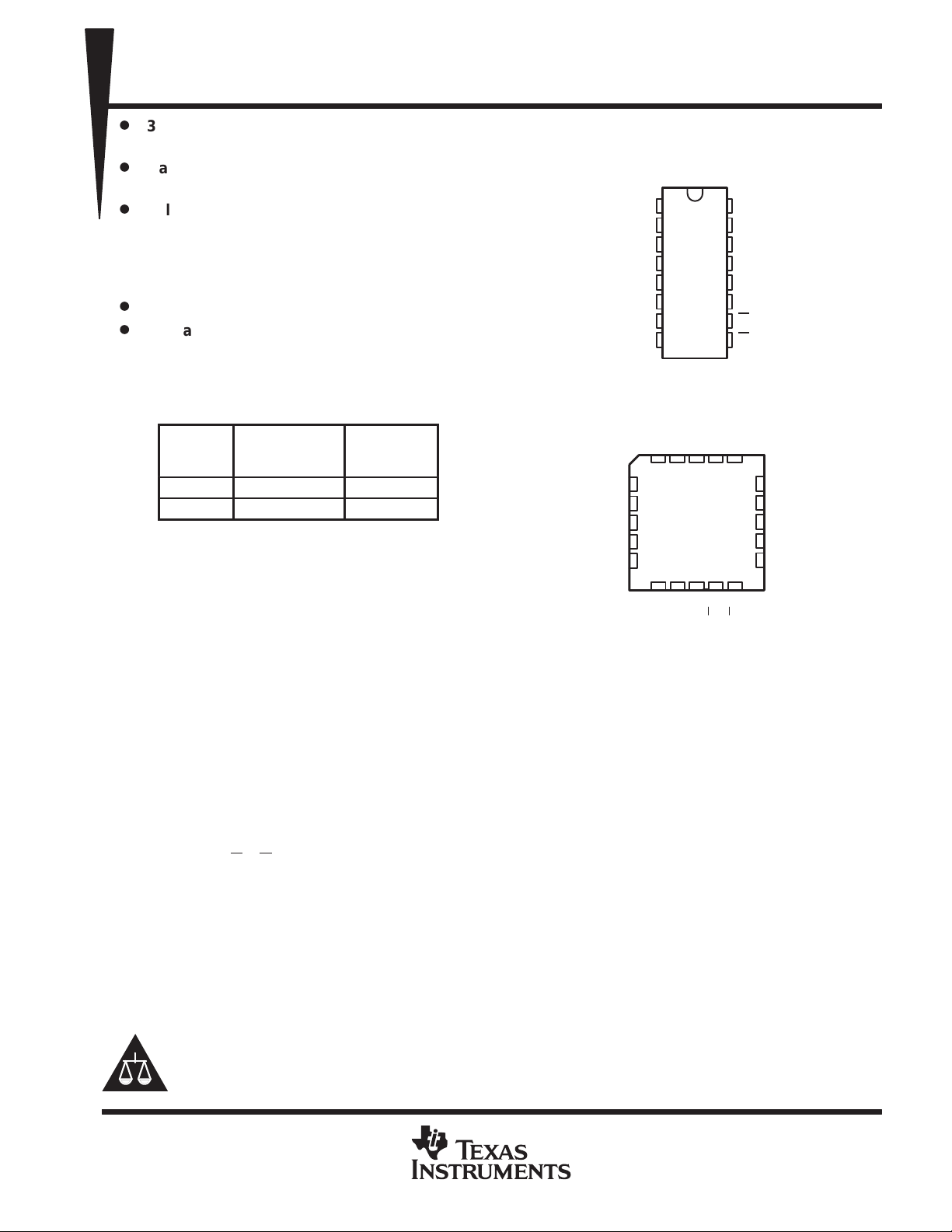
SN54173, SN54LS173A ...J OR W PACKAGE
SN74173 ...N PACKAGE
SN74LS173A ...D or N PACKAGE
(TOP VIEW)
Disabling the Outputs
1
D
Fully Independent Clock Virtually
Eliminates Restrictions for Operating in
One of Two Modes:
– Parallel Load
– Do Nothing (Hold)
D
For Application as Bus Buffer Registers
D
Package Options Include Plastic
Small-Outline (D) Packages, Ceramic Flat
M
N
1Q
2Q
3Q
4Q
CLK
GND
16
V
15
14
13
12
11
10
CC
CLR
1D
2D
3D
4D
2
G
9
G
1
2
3
4
5
6
7
8
(W) Packages, Ceramic Chip Carriers (FK),
and Standard Plastic (N) and Ceramic (J)
DIPs
TYPICAL
TYPE
’173 23 ns 35 MHz
’LS173A 18 ns 50 MHz
PROPAGATION
DELAY TIME
MAXIMUM
CLOCK
FREQUENCY
description
The ’173 and ’LS173A 4-bit registers include
SN54LS173A . . . FK PACKAGE
(TOP VIEW)
V
CC
CLR
18
17
16
15
14
1Q
2Q
NC
3Q
4Q
NMNC
3212019
4
5
6
7
8
910111213
1D
2D
NC
3D
4D
D-type flip-flops featuring totem-pole 3-state
outputs capable of driving highly capacitive
or relatively low-impedance loads. The
high-impedance third state and increased
CLK
GND
NC – No internal connection
NC
G1
G2
high-logic-level drive provide these flip-flops with
the capability of being connected directly to and
driving the bus lines in a bus-organized system without need for interface or pull-up components. Up to 128 of
the SN74173 or SN74LS173A outputs can be connected to a common bus and still drive two Series 54/74 or
54LS/74LS TTL normalized loads, respectively . Similarly, up to 49 of the SN54173 or SN54LS173A outputs can
be connected to a common bus and drive one additional Series 54/74 or 54LS/74LS TTL normalized load,
respectively. To minimize the possibility that two outputs will attempt to take a common bus to opposite logic
levels, the output control circuitry is designed so that the average output disable times are shorter than the
average output enable times.
Gated enable inputs are provided on these devices for controlling the entry of data into the flip-flops. When both
data-enable (G
1, G2) inputs are low, data at the D inputs are loaded into their respective flip-flops on the next
positive transition of the buffered clock input. Gate output-control (M, N) inputs also are provided. When both
are low, the normal logic states (high or low levels) of the four outputs are available for driving the loads or bus
lines. The outputs are disabled independently from the level of the clock by a high logic level at either
output-control input. The outputs then present a high impedance and neither load nor drive the bus line. Detailed
operation is given in the function table.
The SN54173 and SN54LS173A are characterized for operation over the full military temperature range of
–55°C to 125°C. The SN74173 and SN74LS173A are characterized for operation from 0°C to 70°C.
Please be aware that an important notice concerning availability, standard warranty, and use in critical applications of
Texas Instruments semiconductor products and disclaimers thereto appears at the end of this data sheet.
PRODUCTION DATA information is current as of publication date.
Products conform to specifications per the terms of Texas Instruments
standard warranty. Production processing does not necessarily include
testing of all parameters.
POST OFFICE BOX 655303 • DALLAS, TEXAS 75265
Copyright 1999, Texas Instruments Incorporated
On products compliant to MIL-PRF-38535, all parameters are tested
unless otherwise noted. On all other products, production
processing does not necessarily include testing of all parameters.
1
SN54173, SN54LS173A, SN74173, SN74LS173A
CLR
CLK
Q
4-BIT D-TYPE REGISTERS
WITH 3-STATE OUTPUTS
SDLS067A – OCTOBER 1976 – REVISED JUNE 1999
FUNCTION TABLE
INPUTS
DATA ENABLE
G1 G2
H X X X X L
L LXXX Q
L↑HXX Q
L↑XHX Q
L↑L
L↑LLH H
When either M or N (or both) is (are) high, the output is
disabled to the high-impedance state; however, sequential
operation of the flip-flops is not affected.
DATA
L
D
L
OUTPUT
0
0
0
L
15
1
2
9
10
7
14
13
12
11
†
’173 ’LS173A
R
&
&
1D
EN
C1
3
1Q
4
2Q
5
3Q
6
4Q
CLR
G
G2
CLK
1D
2D
3D
4D
15
1
M
2
N
9
1
10
7
14
13
12
11
R
&
EN
&
C1
1D
logic symbol
CLR
M
N
G
1
2
G
CLK
1D 1Q
2D
3D
4D
†
This symbol is in accordance with ANSI/IEEE Standard 91-1984 and IEC Publication 617-12.
Pin numbers shown are for D, J, N, and W packages.
3
4
2Q
5
3Q
6
4Q
2
POST OFFICE BOX 655303 • DALLAS, TEXAS 75265
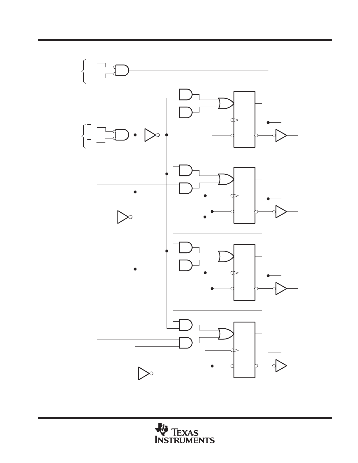
logic diagram (positive logic)
1
Output
Control
M
2
N
SN54173, SN54LS173A, SN74173, SN74LS173A
4-BIT D-TYPE REGISTERS
WITH 3-STATE OUTPUTS
SDLS067A – OCTOBER 1976 – REVISED JUNE 1999
Data
Enable
1D
G
G
2D
CLK
3D
14
9
1
10
2
13
7
12
1D
R
1D
R
1D
C1
C1
3
1Q
4
2Q
11
4D
15
CLR
Pin numbers shown are for D, J, N, and W packages.
R
1D
R
C1
C1
5
3Q
6
4Q
POST OFFICE BOX 655303 • DALLAS, TEXAS 75265
3
SN54173, SN54LS173A, SN74173, SN74LS173A
4-BIT D-TYPE REGISTERS
WITH 3-STATE OUTPUTS
SDLS067A – OCTOBER 1976 – REVISED JUNE 1999
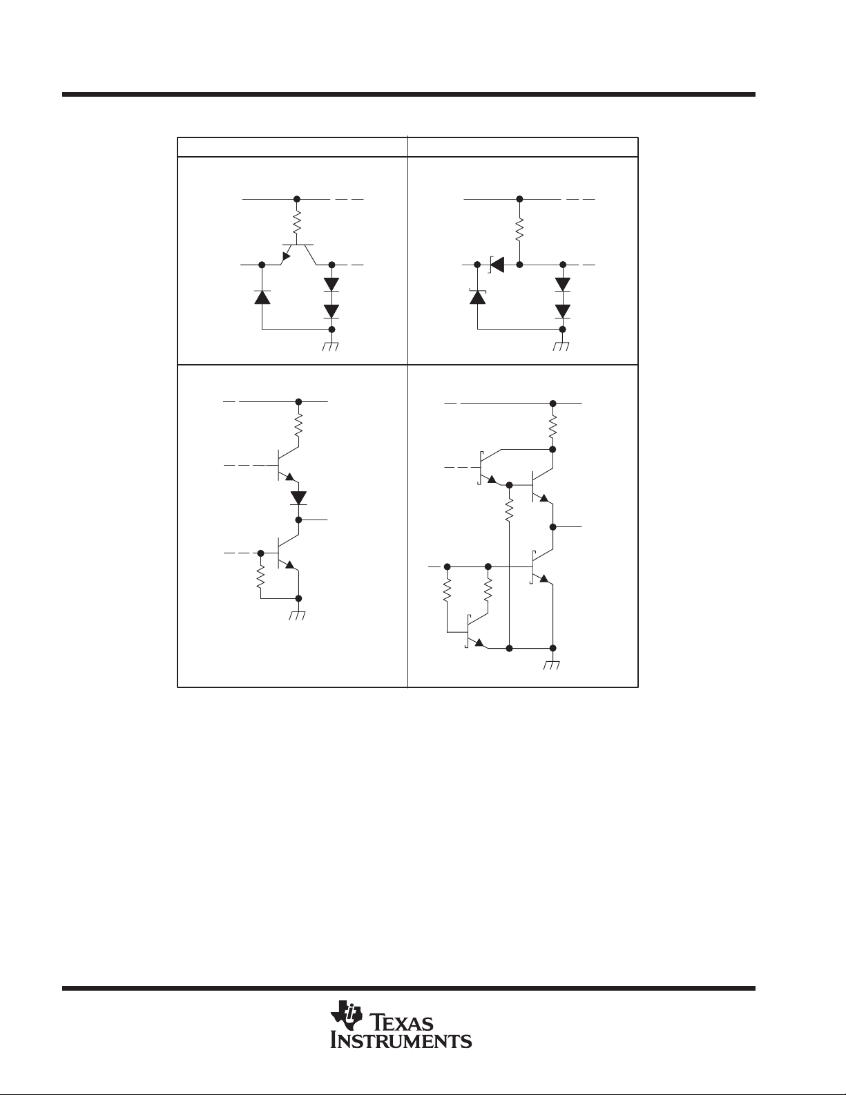
schematics of inputs and outputs
’173 ’LS173A
Equivalent of Each Input Equivalent of Each Input
V
CC
4 kΩ NOM
V
CC
20 kΩ NOM
Input
Typical of All Outputs
V
CC
90 Ω NOM
Output
Input
Typical of All Outputs
V
CC
100 Ω NOM
Output
absolute maximum ratings over operating free-air temperature range (unless otherwise noted)
Supply voltage, V
Input voltage: ’173 –0.5 V to 5.5 V. . . . . . . . . . . . . . . . . . . . . . . . . . . . . . . . . . . . . . . . . . . . . . . . . . . . . . . . . . . . . . . .
Off-state output voltage –0.5 V to 5.5 V. . . . . . . . . . . . . . . . . . . . . . . . . . . . . . . . . . . . . . . . . . . . . . . . . . . . . . . . . . . .
Package thermal impedance, θ
Storage temperature range, T
†
Stresses beyond those listed under “absolute maximum ratings” may cause permanent damage to the device. These are stress ratings only, and
functional operation of the device at these or any other conditions beyond those indicated under “recommended operating conditions” is not
implied. Exposure to absolute-maximum-rated conditions for extended periods may affect device reliability.
NOTES: 1. Voltage values are with respect to network ground terminal.
4
2. The package thermal impedance is calculated in accordance with JESD 51, except for through-hole packages, which use a trace
length of zero.
(see Note 1) –0.5 V to 7 V. . . . . . . . . . . . . . . . . . . . . . . . . . . . . . . . . . . . . . . . . . . . . . . . . . . .
CC
’LS173A –0.5 V to 7 V. . . . . . . . . . . . . . . . . . . . . . . . . . . . . . . . . . . . . . . . . . . . . . . . . . . . . . . . . . . . .
(see Note 2): D package 113°C/W. . . . . . . . . . . . . . . . . . . . . . . . . . . . . . . . . .
JA
N package 78°C/W. . . . . . . . . . . . . . . . . . . . . . . . . . . . . . . . . . .
–65°C to 150°C. . . . . . . . . . . . . . . . . . . . . . . . . . . . . . . . . . . . . . . . . . . . . . . . . . .
stg
POST OFFICE BOX 655303 • DALLAS, TEXAS 75265
†

UNIT
PARAMETER
TEST CONDITIONS
†
UNIT
I
(g )
CC
,
A
UNIT
thHold time
ns
SN54173, SN54LS173A, SN74173, SN74LS173A
4-BIT D-TYPE REGISTERS
WITH 3-STATE OUTPUTS
SDLS067A – OCTOBER 1976 – REVISED JUNE 1999
recommended operating conditions (see Note 3)
SN54173 SN74173
MIN NOM MAX MIN NOM MAX
V
I
OH
I
OL
T
NOTE 3: All unused inputs of the device must be held at VCC or GND to ensure proper device operation. Refer to the TI application report,
electrical characteristics over recommended operating free-air temperature range (unless
otherwise noted)
V
V
V
V
V
O(off)
I
I
I
IH
I
IL
I
OS
I
CC
†
For conditions shown as MIN or MAX, use the appropriate value specified under recommended operating conditions.
‡
All typical values are at VCC = 5 V, TA = 25°C.
§
Not more than one output should be shorted at a time.
NOTE 4: ICC is measured with all outputs open; CLR grounded, following momentary connection to 4.5 V , N, G
Supply voltage 4.5 5 5.5 4.75 5 5.25 V
CC
High-level output current –2 –5.2 mA
Low-level output current 16 16 mA
Operating free-air temperature –55 125 0 70 °C
A
Implications of Slow or Floating CMOS Inputs,
High-level input voltage 2 2 V
IH
Low-level input voltage 0.8 0.8 V
IL
Input clamp voltage VCC = MIN, II = –12 mA –1.5 –1.5 V
IK
High-level output voltage
OH
Low-level output voltage
OL
Off-state (high-impedance state) V
output current
Input current
at maximum input voltage
High-level input current VCC = MAX, VI = 2.4 V 40 40 µA
Low-level input current VCC = MAX, VI = 0.4 V –1.6 –1.6 mA
Short-circuit output current
Supply current VCC = MAX, See Note 4 50 72 50 72 mA
and CLK and M at 4.5 V.
§
literature number SCBA004.
SN54173 SN74173
MIN TYP‡MAX MIN TYP‡MAX
VCC = MIN,
VIL = 0.8 V,
VCC = MIN,
VIL = 0.8 V,
= MAX,
VIH = 2 V
VCC = MAX, VI = 5.5 V 1 1 mA
VCC = MAX –30 –70 –30 –70 mA
VIH = 2 V,
IOH = MAX
VIH = 2 V,
IOL = 16 mA
VO = 2.4 V 150 40
VO = 0.4 V –150 –40
2.4 2.4 V
0.4 0.4 V
1, G2, and all data inputs grounded;
µ
timing requirements over recommended operating conditions (unless otherwise noted)
SN54173 SN74173
MIN MAX MIN MAX
f
clock
t
w
t
su
Input clock frequency 25 25 MHz
Pulse duration CLK or CLR 20 20 ns
Data enable (G1, G2) 17 17
Setup time
POST OFFICE BOX 655303 • DALLAS, TEXAS 75265
Data
CLR (inactive state) 10 10
Data enable (G1, G2) 2 2
Data 10 10
10 10
ns
5

SN54173, SN54LS173A, SN74173, SN74LS173A
PARAMETER
TEST CONDITIONS
UNIT
L
ns
ns
C
pF
ns
4-BIT D-TYPE REGISTERS
WITH 3-STATE OUTPUTS
SDLS067A – OCTOBER 1976 – REVISED JUNE 1999
switching characteristics, VCC = 5 V, TA = 25°C, R
f
max
t
PHL
t
PLH
t
PHL
t
PZH
t
PZL
t
PHZ
t
PLZ
Maximum clock frequency 25 35 25 35 MHz
Propagation delay time,
high-to-low-level output from clear input
Propagation delay time,
low-to-high-level output from clock input
Propagation delay time,
high-to-low-level output from clock input
Output enable time to high level 7 16 30 7 16 30
Output enable time to low level 7 21 30 7 21 30
Output disable time from high level
Output disable time from low level
C
= 50 pF
L
= 5
p
= 400 Ω (see Figure 1)
L
SN54173 SN74173
MIN TYP MAX MIN TYP MAX
18 27 18 27 ns
28 43 28 43
19 31 19 31
3 5 14 3 5 14
3 11 20 3 11 20
6
POST OFFICE BOX 655303 • DALLAS, TEXAS 75265

UNIT
PARAMETER
TEST CONDITIONS
†
VOLLow-level output voltage
CC
,
I
(g )
CC
,
V
UNIT
thHold time
ns
SN54173, SN54LS173A, SN74173, SN74LS173A
4-BIT D-TYPE REGISTERS
WITH 3-STATE OUTPUTS
SDLS067A – OCTOBER 1976 – REVISED JUNE 1999
recommended operating conditions
SN54LS173A SN74LS173A
MIN NOM MAX MIN NOM MAX
V
I
OH
I
OL
T
electrical characteristics over recommended operating free-air temperature range (unless
otherwise noted)
V
V
V
V
O(off)
I
I
I
IH
I
IL
I
OS
I
CC
†
For conditions shown as MIN or MAX, use the appropriate value specified under recommended operating conditions.
‡
All typical values are at VCC = 5 V, TA = 25°C.
§
Not more than one output should be shorted at a time.
NOTE 4: ICC is measured with all outputs open; CLR grounded, following momentary connection to 4.5 V , N, G
Supply voltage 4.5 5 5.5 4.75 5 5.25 V
CC
High-level output current –1 –2.6 mA
Low-level output current 12 24 mA
Operating free-air temperature –55 125 0 70 °C
A
SN54LS173A SN74LS173A UNIT
MIN TYP‡MAX MIN TYP‡MAX UNIT
High-level input voltage 2 2 V
IH
Low-level input voltage 0.7 0.8 V
IL
Input clamp voltage VCC = MIN, II = –18 mA –1.5 –1.5 V
IK
High-level output voltage
OH
p
Off-state (high-impedance state) V
output current
Input current
at maximum input voltage
High-level input current VCC = MAX, VI = 2.7 V 20 20 µA
Low-level input current VCC = MAX, VI = 0.4 V –0.4 –0.4 mA
Short-circuit output current
Supply current VCC = MAX, See Note 4 19 30 19 24 mA
and CLK and M at 4.5 V.
§
VCC = MIN,
VIL = VILmax,
V
= MIN,
VIL = 0.8 V,
= MAX,
VIH = 2 V
VCC = MAX, VI = 7 V 0.1 0.1 mA
VCC = MAX –30 –130 –30 –130 mA
VIH = 2 V,
IOH = MAX
IOL = 12 mA 0.25 0.4 0.25 0.4 V
IOL = 24 mA 0.35 0.5 V
VO = 2.7 V 20 20
VO = 0.4 V –20 –20
2.4 3.4 2.4 3.1 V
1, G2, and all data inputs grounded;
timing requirements over recommended operating conditions (unless otherwise noted)
f
clock
t
w
t
su
SN54LS173A SN74LS173A
MIN MAX MIN MAX
Input clock frequency 30 25 MHz
Pulse duration CLK or CLR 25 25 ns
Data enable (G1, G2) 35 35
Setup time
POST OFFICE BOX 655303 • DALLAS, TEXAS 75265
Data 17 17
CLR (inactive state) 10 10
Data enable (G1, G2) 0 0
Data 3 3
ns
7

SN54173, SN54LS173A, SN74173, SN74LS173A
PARAMETER
TEST CONDITIONS
UNIT
L
ns
ns
C
pF
ns
4-BIT D-TYPE REGISTERS
WITH 3-STATE OUTPUTS
SDLS067A – OCTOBER 1976 – REVISED JUNE 1999
switching characteristics, VCC = 5 V, TA = 25°C, R
f
max
t
PHL
t
PLH
t
PHL
t
PZH
t
PZL
t
PHZ
t
PLZ
Maximum clock frequency 30 50 30 50 MHz
Propagation delay time,
high-to-low-level output from clear input
Propagation delay time,
low-to-high-level output from clock input
Propagation delay time,
high-to-low-level output from clock input
Output enable time to high level 15 23 15 23
Output enable time to low level 18 27 18 27
Output disable time from high level
Output disable time from low level
C
= 45 pF
L
= 5
p
= 667 Ω (see Figure 2)
L
SN54LS173A SN74LS173A
MIN TYP MAX MIN TYP MAX
26 35 26 35 ns
17 25 17 25
22 30 22 30
11 20 11 20
11 17 11 17
8
POST OFFICE BOX 655303 • DALLAS, TEXAS 75265

From Output
Under Test
(see Note A)
Test
Point
C
L
SN54173, SN54LS173A, SN74173, SN74LS173A
PARAMETER MEASUREMENT INFORMATION
SERIES 54/74 AND 54S/74S DEVICES
V
CC
V
CC
R
L
R
(see Note B)
From Output
Under Test
(see Note A)
C
L
L
Test
Point
4-BIT D-TYPE REGISTERS
WITH 3-STATE OUTPUTS
SDLS067A – OCTOBER 1976 – REVISED JUNE 1999
V
CC
From Output
Under Test
(see Note A)
Test
Point
C
L
1 kΩ
R
L
S1
(see
Note B)
S2
FOR 2-STATE TOTEM-POLE OUTPUTS
High-Level
Low-Level
In-Phase
Output
(see Note D)
Out-of-Phase
Output
(see Note D)
LOAD CIRCUIT
Pulse
Pulse
VOLTAGE WAVEFORMS
Input
t
PLH
t
PHL
VOLTAGE WAVEFORMS
PROPAGATION DELAY TIMES
1.5 V 1.5 V
1.5 V 1.5 V
PULSE DURATIONS
1.5 V 1.5 V
1.5 V
1.5 V 1.5 V
t
w
t
PHL
1.5 V
t
PLH
FOR OPEN-COLLECTOR OUTPUTS
3 V
0 V
V
OH
V
OL
V
OH
V
OL
LOAD CIRCUIT
Timing
Input
t
Data
Input
Output
Control
(low-level
enabling)
t
PZL
Waveform 1
(see Notes C
and D)
t
PZH
Waveform 2
(see Notes C
and D)
ENABLE AND DISABLE TIMES, 3-STATE OUTPUTS
FOR 3-STATE OUTPUTS
1.5 V
su
1.5 V 1.5 V
VOLTAGE WAVEFORMS
SETUP AND HOLD TIMES
1.5 V
1.5 V
1.5 V
VOLTAGE WAVEFORMS
LOAD CIRCUIT
3 V
0 V
t
h
3 V
0 V
1.5 V
t
PLZ
t
PHZ
3 V
0 V
≈1.5 V
VOL + 0.5 V
V
OL
V
OH
VOH – 0.5 V
≈1.5 V
NOTES: A. CL includes probe and jig capacitance.
B. All diodes are 1N3064 or equivalent.
C. Waveform 1 is for an output with internal conditions such that the output is low except when disabled by the output control.
Waveform 2 is for an output with internal conditions such that the output is high except when disabled by the output control.
D. S1 and S2 are closed for t
E. All input pulses are supplied by generators having the following characteristics: PRR ≤ 1 MHz, ZO ≈ 50 Ω, tr and tf ≤7 ns for Series
54/74 devices and tr and tf ≤ 2.5 ns for Series 54S/74S devices.
F. The outputs are measured one at a time with one input transition per measurement.
PLH
, t
PHL
, t
Figure 1. Load Circuits and Voltage Waveforms
POST OFFICE BOX 655303 • DALLAS, TEXAS 75265
PHZ
, and t
; S1 is open and S2 is closed for t
PLZ
; S1 is closed and S2 is open for t
PZH
PZL
.
9

SN54173, SN54LS173A, SN74173, SN74LS173A
4-BIT D-TYPE REGISTERS
WITH 3-STATE OUTPUTS
SDLS067A – OCTOBER 1976 – REVISED JUNE 1999
PARAMETER MEASUREMENT INFORMATION
SERIES 54LS/74LS DEVICES
From Output
Under Test
(see Note A)
TOTEM-POLE OUTPUTS
High-Level
Pulse
Low-Level
Pulse
Test
Point
C
L
LOAD CIRCUIT FOR
2-STATE
1.3 V 1.3 V
1.3 V 1.3 V
VOLTAGE WAVEFORMS
PULSE DURATIONS
V
CC
R
(see Note B)
t
w
V
CC
V
L
From Output
Under Test
(see Note A)
LOAD CIRCUIT
FOR OPEN-COLLECTOR OUTPUTS
CC
R
L
Test
Point
C
L
Timing
Input
Data
Input
From Output
Under Test
(see Note A)
1.3 V
t
su
1.3 V 1.3 V
VOLTAGE WAVEFORMS
SETUP AND HOLD TIMES
Test
Point
C
L
LOAD CIRCUIT
FOR 3-STATE OUTPUTS
t
h
5 kΩ
3 V
0 V
3 V
0 V
R
L
S1
(see
Note B)
S2
Input
t
PLH
In-Phase
Output
(see Note D)
t
PHL
Out-of-Phase
Output
(see Note D)
NOTES: A. CL includes probe and jig capacitance.
B. All diodes are 1N3064 or equivalent.
C. Waveform 1 is for an output with internal conditions such that the output is low except when disabled by the output control.
Waveform 2 is for an output with internal conditions such that the output is high except when disabled by the output control.
D. S1 and S2 are closed for t
E. Phase relationships between inputs and outputs have been chosen arbitrarily for these examples.
F. All input pulses are supplied by generators having the following characteristics: PRR ≤ 1 MHz, ZO ≈ 50 Ω, tr ≤ 15 ns, tf ≤ 6 ns.
G. The outputs are measured one at a time with one input transition per measurement.
1.3 V 1.3 V
1.3 V 1.3 V
1.3 V 1.3 V
VOLTAGE WAVEFORMS
PROPAGATION DELAY TIMES
, t
PLH
PHL
t
t
PLH
, t
PHL
PHZ
3 V
0 V
V
V
V
V
OH
OL
OH
OL
, and t
Output
Control
(low-level
enabling)
t
PZL
Waveform 1
S2 Open
(see Notes C
and D)
t
PZH
Waveform 2
S2 Closed
(see Notes C
and D)
ENABLE AND DISABLE TIMES, 3-STATE OUTPUTS
; S1 is open and S2 is closed for t
PLZ
1.3 V 1.3 V
1.3 V
1.3 V
VOLTAGE WAVEFORMS
; S1 is closed and S2 is open for t
PZH
t
PLZ
t
PHZ
3 V
0 V
≈1.5 V
VOL + 0.3 V
V
OL
V
OH
VOH – 0.3 V
≈1.5 V
PZL
.
10
Figure 2. Load Circuits and Voltage Waveforms
POST OFFICE BOX 655303 • DALLAS, TEXAS 75265

IMPORTANT NOTICE
T exas Instruments and its subsidiaries (TI) reserve the right to make changes to their products or to discontinue
any product or service without notice, and advise customers to obtain the latest version of relevant information
to verify, before placing orders, that information being relied on is current and complete. All products are sold
subject to the terms and conditions of sale supplied at the time of order acknowledgement, including those
pertaining to warranty, patent infringement, and limitation of liability.
TI warrants performance of its semiconductor products to the specifications applicable at the time of sale in
accordance with TI’s standard warranty. Testing and other quality control techniques are utilized to the extent
TI deems necessary to support this warranty . Specific testing of all parameters of each device is not necessarily
performed, except those mandated by government requirements.
CERT AIN APPLICATIONS USING SEMICONDUCTOR PRODUCTS MAY INVOLVE POTENTIAL RISKS OF
DEATH, PERSONAL INJURY, OR SEVERE PROPERTY OR ENVIRONMENTAL DAMAGE (“CRITICAL
APPLICATIONS”). TI SEMICONDUCTOR PRODUCTS ARE NOT DESIGNED, AUTHORIZED, OR
WARRANTED TO BE SUITABLE FOR USE IN LIFE-SUPPORT DEVICES OR SYSTEMS OR OTHER
CRITICAL APPLICA TIONS. INCLUSION OF TI PRODUCTS IN SUCH APPLICATIONS IS UNDERST OOD TO
BE FULLY AT THE CUSTOMER’S RISK.
In order to minimize risks associated with the customer’s applications, adequate design and operating
safeguards must be provided by the customer to minimize inherent or procedural hazards.
TI assumes no liability for applications assistance or customer product design. TI does not warrant or represent
that any license, either express or implied, is granted under any patent right, copyright, mask work right, or other
intellectual property right of TI covering or relating to any combination, machine, or process in which such
semiconductor products or services might be or are used. TI’s publication of information regarding any third
party’s products or services does not constitute TI’s approval, warranty or endorsement thereof.
Copyright 1999, Texas Instruments Incorporated
 Loading...