

查询SN75LVDS88B供应商
D
Flatlink Interface Utilizes Low Power
Differential Signalling(LVDS)
D
Suitable for Notebook Application
D
XGA Resolution
D
Six Bit System Interface
D
Support Mainstream Data and Gate Drivers
D
Optional Configurable Pins
description
The SN75L VDS88B (LVDS panel timing controller) integrates a Flatlink signal interface with a TFT LCD timing
controller. It resides in the LCD panel and provides interface between the graphic controller and a TFT LCD
panel.
The SN75L VDS88B accepts host data through 3 pairs of inputs (18-bits) making up the LVDS bus, which is a
low-EMI high-throughput interface. SN75L VDS88B then reformats the received image data into a specific data
format and synchronous timing suitable for driving LCD panel column and row drivers. This device supports
XGA resolution.
The SN75LVDS88B is easily configured by several selection terminals and is equipped with default timing
specifications to support mainstream gate and source drivers on the market.
SN75LVDS88B
TFT LCD PANEL TIMING CONTROLLER
WITH LVDS INTERF ACE
SLLS407 – FEBRUARY 2000
D
Low Voltage CMOS 3.3 V T echnology
D
65 MHz Phase-Lock Input
D
100-pin TQFP Package for Compact LCD
Module
D
Tolerates 4 kV HBM ESD for LVDS Pins and
2 kV HBM for Others
D
Improved Jitter Tolerance
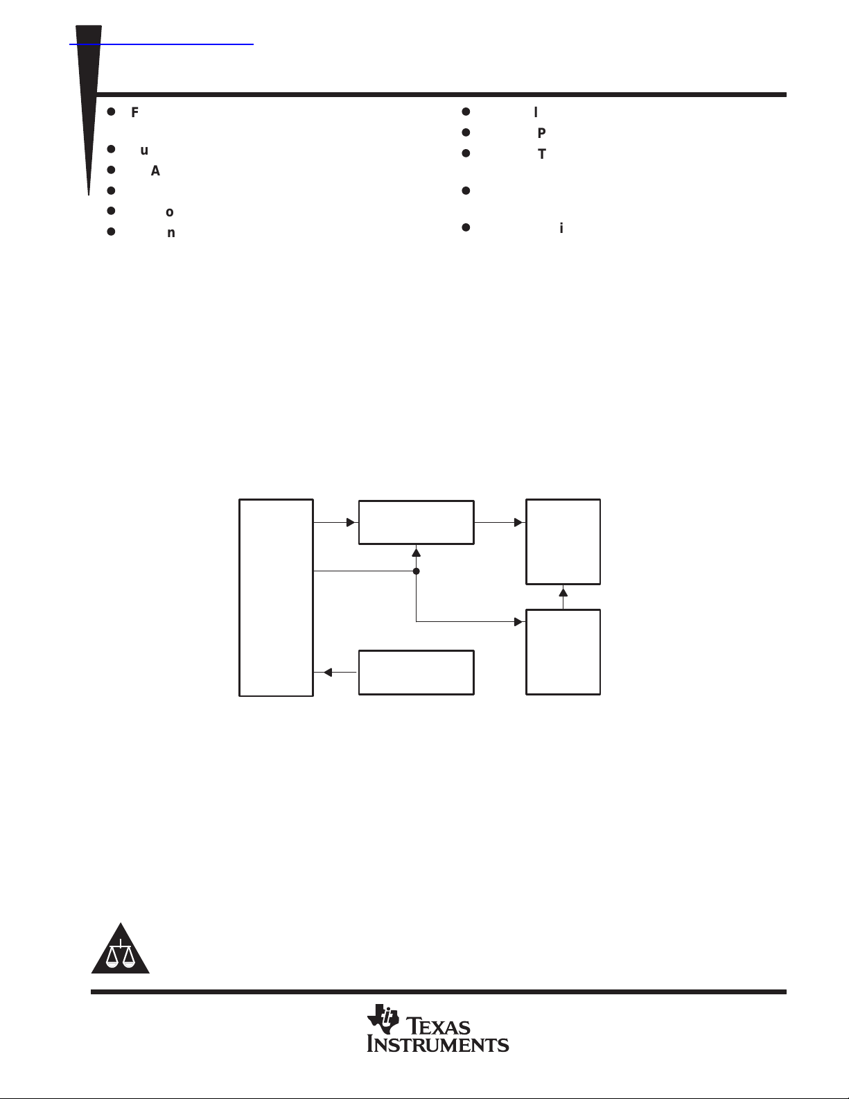
block diagram
Flatlink
(18-bit)
Data Alignment
SYNC
CTRL
Interface
Source
Data
Format
Timing
Signal
Generator
Please be aware that an important notice concerning availability, standard warranty, and use in critical applications of
Texas Instruments semiconductor products and disclaimers thereto appears at the end of this data sheet.
Flatlink is a trademark of Texas Instruments Incorporated.
PRODUCTION DATA information is current as of publication date.
Products conform to specifications per the terms of Texas Instruments
standard warranty. Production processing does not necessarily include
testing of all parameters.
POST OFFICE BOX 655303 • DALLAS, TEXAS 75265
Copyright 2000, Texas Instruments Incorporated
1
SN75LVDS88B
TFT LCD PANEL TIMING CONTROLLER
WITH LVDS INTERF ACE
SLLS407 – FEBRUARY 2000
pin assignment
TQFP PACKAGE
(TOP VIEW)
MODE2
TP1
CPV
VSS
STV
OE1
REV_E
VDD
REV_O
OE2
TP2
VSSIO
CLK
VDDIO
TEST2
ER5(EB5)
VSSIO
ER4(EB4)
ER3(EB3)
VDDIO
ER2(EB2)
ER1(EB1)
VSSIO
ER0(EB0)
EG5
1
2
3
4
5
6
7
8
9
10
11
12
13
14
15
16
17
18
19
20
21
22
23
24
25
TEST1
MODE1NCVSS
98
99
100
28
27
26
DBS
96
97
30
29
POLEN
VDDA
RSTZ
93
94
95
33
32
31
GNDANCCLKP
92
GND1
NC
90
91
89
88
CLKM
87
SN75LVDS88B
38
39
37
36
35
34
A2P
86
40
A2M
85
41
A1P
84
42
A1M
83
43
A0P
82
44
A0M
GNDD
80
81
46
45
SHTDN
VDDDNCNC
77
78
79
49
48
47
76
75
74
73
72
71
70
69
68
67
66
65
64
63
62
61
60
59
58
57
56
55
54
53
52
51
50
VDD
OPOL
VSS
OB0(OR0)
VDD
OB1(OR1)
OB2(OR2)
VSSIO
OB3(OR3)
OB4(OR4)
VDDIO
OB5(OR5)
OG0
VSSIO
OG1
OG2
VDDIO
OG3
OG4
VSSIO
OG5
OR0(OB0)
VDDIO
OR1(OB1)
OR2(OB2)
SP
EG4
EG3
EG2
EG1
EG0
VDDIO
VSSIO
VDDIO
EB5(ER5)
2
POST OFFICE BOX 655303 • DALLAS, TEXAS 75265
VSSIO
EB3(ER3)
EB4(ER4)
EB2(ER2)
VDDIO
EB1(ER1)
EB0(ER0)
EPOL
VSSIO
CLK
VDDIO
VSSIO
OR5(OB3)
OR4(OB4)
OR3(OB3)
I/O
DESCRIPTION
TFT LCD PANEL TIMING CONTROLLER
Terminal Functions
TERMINAL
NAME NO.
A0M/A0P 81,82 I Flatlink 1st data pair
A1M/A1P 83, 84 I Flatlink 2nd data pair
A2M/A2P 85, 86 I Flatlink 3rd data pair
CLK 44 O CD bus clock
CLK 13 O CD bus clock (180 degree out of phase)
CLKM/CLKP 87, 88 I Flatlink clock pair
CPV 3 O Gate driver clock
DBS 97 I Data bus sequence
EPOL 42 O Even RGB data stream polarity indicator
ER0..ER5
(EB0)..(EB5)
(ER0)..(ER5)
EB0..EB5
GND1 91 P PLL ground for LVDS
MODE1 99 I Default timing selection pin 1
MODE2 1 I Default timing selection pin 2
NC 76, 77, 89, 90, 98 NC NC terminals
OE1, OE2 6, 10 O Gate driver output enable
OG0..OG5 63, 61, 60,
OPOL 74 O Odd RGB data stream polarity indicator
OR0..OR5
(OB0)..(OB5)
(OR0)..(OR5)
OB0..OB5
POLEN 95 I Output data polarity control enable /disable
REV_E 7 O CD line/dot inversion control signal
REV_O 9 O CD line/dot inversion control signal (180 degree of phase)
RSTZ 93 I Reset, active low
SHTDN 79 I System shutdown control, active low
SP 46 O Data bus starting pulse
STV 5 O Gate driver starting pulse
TEST1, TEST2 100, 15 I Test points
TP1, TP2 2, 11 O CD output control signal
VDDA 94 P PLL power for LVDS
GNDA 92 P Analog ground for LVDS
VDDD 78 P Digital power supply for LVDS
GNDD 80 P Digital power ground for L VDS
VDD 8,71,75 P Digital power
VSS 4,73,96 P Digital ground
VDDIO 14, 20, 28, 34,
VSSIO 12, 17, 23, 31,
†
Terminals must be connected to ground.
24, 22, 21,
19, 18, 16
41,39,38
36,35,33
58, 57, 55
54, 52, 51,
50, 49, 47
72, 70, 69
67, 66, 64
40, 45, 53, 59, 65
37, 43, 48, 56,
62, 68
O Even red (blue) data bus, controlled by DBS Pin, 0 = red, 1 = blue
O Even blue (red) data bus, controlled by DBS Pin, 0 = blue, 1 = red
†
O Odd green data bus
O Odd red (blue) data bus, controlled by DBS Pin, 0 = red, 1 = blue
O Odd blue (red) data bus, controlled by DBS Pin, 0 = blue, 1 = red
†
P I/O power
P I/O ground
SN75LVDS88B
WITH LVDS INTERF ACE
SLLS407 – FEBRUARY 2000
POST OFFICE BOX 655303 • DALLAS, TEXAS 75265
3
SN75LVDS88B
PIN NAME
PIN NO
DESCRIPTION
TFT LCD PANEL TIMING CONTROLLER
WITH LVDS INTERF ACE
SLLS407 – FEBRUARY 2000
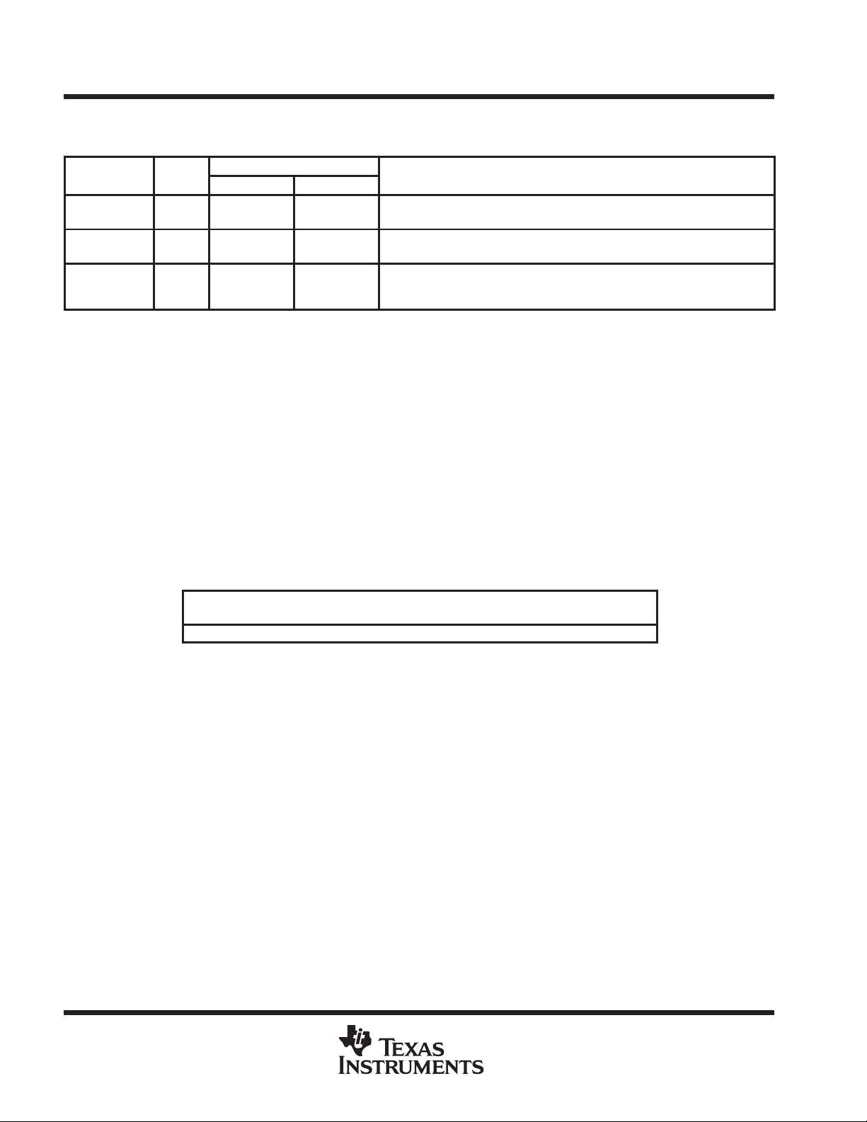
options
output control
INTERNAL CONNECTION
.
REQUIRED SUGGESTED
MODE1
MODE2
POLEN Pulldown 0 = Output data reverse disable
DBS 97 Pulldown Data bus sequence
NOTE: NC pin 76 is internally pulldown and NC pins 77 and 98 are internally pullup.
991Pullup
Pulldown
Default timing selection pin 1
Default timing selection pin 2
1 = Output data reverse enable
0 = normal (RGB)
1 = reverse (BGR)
CC
†
+ 0.5 V. . . . . . . . . . . . . . . . . . . . . . . . . . . . . . . . . . . . . . . . . . . . . . . . .
absolute maximum ratings over operating free-air temperature (unless otherwise noted)
Supply voltage range, V
Voltage range at any terminal –0.5 V to V
‡
–0.5 V to 4 V. . . . . . . . . . . . . . . . . . . . . . . . . . . . . . . . . . . . . . . . . . . . . . . . . . . . . . . . .
CC
Continuous power dissipation See Dissipation Rating Table. . . . . . . . . . . . . . . . . . . . . . . . . . . . . . . . . . . . . . . . .
Storage temperature range, T
–65°C to 150°C. . . . . . . . . . . . . . . . . . . . . . . . . . . . . . . . . . . . . . . . . . . . . . . . . . .
stg
Electrostatic discharge: Class 3 A 4 kV. . . . . . . . . . . . . . . . . . . . . . . . . . . . . . . . . . . . . . . . . . . . . . . . . . . . . . . . . .
Class 2 B 200 V. . . . . . . . . . . . . . . . . . . . . . . . . . . . . . . . . . . . . . . . . . . . . . . . . . . . . . . . .
Lead temperature 1,6 mm (1/16 inch) from case for 10 seconds 260°C. . . . . . . . . . . . . . . . . . . . . . . . . . . . . . .
†
Stresses beyond those listed under “absolute maximum ratings” may cause permanent damage to the device. These are stress ratings only, and
functional operation of the device at these or any other conditions beyond those indicated under “recommended operating conditions” is not
implied. Exposure to absolute-maximum-rated conditions for extended periods may affect device reliability.
‡
All voltage values are with respect to the GND terminals unless otherwise noted.
DISSIPATION RATING TABLE
PACKAGE
PFD 1.548 W 12 mW 1.012 W
§
This is the inverse of the junction-to-ambient thermal resistance when board-mounted and with
no air flow.
TA ≤ 25°C
POWER RATING
OPERATING FACTOR
ABOVE TA = 25°C
§
TA = 70°C
POWER RATING
4
POST OFFICE BOX 655303 • DALLAS, TEXAS 75265

SHTDN
V
SN75LVDS88B
TFT LCD PANEL TIMING CONTROLLER
WITH LVDS INTERF ACE
SLLS407 – FEBRUARY 2000
recommended operating conditions
MIN NOM MAX UNIT
Supply voltage, V
High-level input voltage, V
Low-level input voltage, V
Magnitude of differential input voltage, VID 0.1 0.6 V
Common–mode input voltage, V
CC
IH
IL
IC
electrical characteristics over recommended operating free-air temperature range (unless
otherwise noted)
PARAMETER TEST CONDITIONS MIN TYP†MAX UNIT
V
Positive-going differential input voltage threshold 100 mV
IT+
V
Negative-going differential input voltage threshold –100 mV
IT–
Disabled, all inputs to ground 360 µA
Enabled, AnP at 1 V and
AnM at 1.4 V, tC = 15.38 ns
I
Quiescent current (average)
CC
I
High-level input current (SHTDN) VIH = V
IH
I
Low-level input current (SHTDN) VIL = 0 V ±20 µA
IL
I
Input current (A inputs) 0 V < VI < 2.4 V ±20 µA
IN
I
High-impendance output current VO = 0 V or V
OZ
†
All typical values are at VCC = 3.3 V, TA = 25°C.
‡
The algebraic convention, in which the less-positive (more-negative) limit is designated minimum, is used in this data sheet for the negative-going
input voltage threshold only .
Enabled, CL = 8 pF,
Grayscale pattern , tC = 15.38 ns
Enabled, CL = 8 pF,
Worst-case pattern, tC = 15.38 ns
CC
CC
3 3.3 3.6 V
2
0.8
|VID|
2
2.4 –
80
100
120
|VID|
2
mA
±20 µA
±10 µA
V
timing requirements
MIN TYP MAX UNIT
§
t
c
tsu/t
§
tc is defined as the mean duration of a minimum of 32,000 clock periods.
Input clock period 14.7 31.25 ns
Input set up or hold time 550 ps
h
output buffer rating
MIN TYP MAX UNIT
STV, SP 4 mA
CLK, CLK 8 mA
Data bus and remaining outputs 4 mA
POST OFFICE BOX 655303 • DALLAS, TEXAS 75265
5

SN75LVDS88B
C
pF
C
80 pF
C
pF
TFT LCD PANEL TIMING CONTROLLER
WITH LVDS INTERF ACE
SLLS407 – FEBRUARY 2000
switching characteristics
PARAMETER TEST CONDITIONS MIN TYP MAX UNIT
t
dr1
t
df1
t
su1
t
h1
t
(RSKM)
t
en
t
dis
t
su2
t
h2
NOTES: 1. t
Input clock rising to output clock rising delay
Input clock rising to output clock falling delay
Data setup time, E/O RGB to CLK↑
Data hold time, CLK↑ to E/O RGB
Receiver input skew margin, See Note 1
Enable time, SHTDN to phase lock 1 ms
Disable time, SHTDN to off state 250 ns
SP setup time
SP pulse hold time
is the timing margin available to allocate to the transmitter and interconnection skews and clock jitter. The value of this
RSKM
parameter at clock periods other than 15.38 ns can be calculated from t
2. |Input clock jitter| is the magnitude of the change in the input clock period.
p
= 80
L
p
=
L
tc = 15.38 ns (+0.2%),
Input clock jitter < 50 ps, See Note 2
p
= 10
sp
t
c
–300 ps.
+
RSKM
14
10 40 ns
10 40 ns
10 20 ns
10 20 ns
550 700 ps
10 20 ns
10 20 ns
CLKM/P
CLK
RGB
SP
PARAMETER MEASUREMENT INFORMATION
t
dr1
t
su1
t
su2
Figure 1. Output Setup and Hold Time
t
dr1
t
t
h
h2
6
POST OFFICE BOX 655303 • DALLAS, TEXAS 75265

reference timing diagrams
horizonal timing
DE
E/OSP
O/ERGB
CPV
TP1
SN75LVDS88B
TFT LCD PANEL TIMING CONTROLLER
WITH LVDS INTERF ACE
SLLS407 – FEBRUARY 2000
PARAMETER MEASUREMENT INFORMATION
TP2
OE1
OE2
REV
vertical timing
DE
TP
Figure 2. Typical Output Waveform
POST OFFICE BOX 655303 • DALLAS, TEXAS 75265
7

SN75LVDS88B
TFT LCD PANEL TIMING CONTROLLER
WITH LVDS INTERF ACE
SLLS407 – FEBRUARY 2000
PARAMETER MEASUREMENT INFORMATION
functional description
Flatlink
The core of the Flatlink is TIs original 86A L VDS receiver, which has three data channels for the 18-bit color plus
one clock channel.
data alignment
The data alignment block supports dual bus, dual port column driver configuration. When interfacing a 2-port
column driver, the controller arranges pixels in odd and even order , then distributes them to odd and even buses
and each connects to either of the driver ports. Under this setup, the controller outputs one clock, one or two
data polarities (depends on driver), and one inverse ( support line inversion) signal to the drivers.
output formatting
The output formatting provides several functions to reduce EMI, noise, and timing delay arrangement. These
functions are controllable through some optional pins. See the registers and options section for reference.
D
Reverse Polarity Generation
When enabled this function generates polarity indication signals. This occurs when the number of
transitions in the output data bus exceeds 18-bits compared to the previous output under normal polarity.
The polarity signal will be active and the output will be the opposite polarity to reduce transition.
D
Line Inversion
When enabled, the REV_O and REV_E terminals will output the same line inversion control signals but in
opposite polarities.
timing control
D
Horizontal Starting pulses
ESP and OSP terminals are used as the horizontal starting pulses output pins. Their outputs are one HCLK
period ahead of the RGB data stream
D
Horizontal Clock
ECLK and OCLK terminals are responsible for the clock pulses, based on the XGA resolution when its
frequency is at 32.5 MHz.
D
CD Data Latch Pulse
TP1 and TP2 provide the column driver input latch and output enable signals.
D
Gate Driver Clock
The CPV terminal output the clock pulses to the gate drivers as the horizontal sync timing in its CRT counter
part.
D
Gate Driver Starting Pulse
The vertical starting pulse automatically generates at the start of every frame.
D
Gate Driver Output Enable
The OE1 and OE2 terminals provide the gate output enabale signals.
8
POST OFFICE BOX 655303 • DALLAS, TEXAS 75265

SN75LVDS88B
TFT LCD PANEL TIMING CONTROLLER
WITH LVDS INTERF ACE
SLLS407 – FEBRUARY 2000
PARAMETER MEASUREMENT INFORMATION
functional description (continued)
vertical/horizontal reference generator
This block provides vertical and horizontal reference points for timing control. Vsync, Hsync, and ENAB signals,
along with the auto detection function, determine when the video from the host is valid.
power-up procedure
Due to the uncertainty of registers and counters in the driver, SN75LVDS88B combines the input from both reset
and Vsync to blank the output and simultaneously resets the content of drivers (see Figure 3).
V
SYNC
RSTZ
OE
Figure 3. Reset Waveform
It is recommended that the following circuit be used to ensure the device is reset for more than 5 ms after power
up.
10 kΩ
RSTZ
4.7 µF
POST OFFICE BOX 655303 • DALLAS, TEXAS 75265
9

SN75LVDS88B
TFT LCD PANEL TIMING CONTROLLER
WITH LVDS INTERF ACE
SLLS407 – FEBRUARY 2000
APPLICATION INFORMATION
SN75LVDS88B
ERGB
ORGB
REV_E/O
CLK
CLK
SP
ORGB
ERGB
SP
CD1 CD2CD3CD4
Figure 4. Application Block Diagram
7135 911
8246 1012
Figure 5. Data Output Format
10
POST OFFICE BOX 655303 • DALLAS, TEXAS 75265
SN75LVDS88B
TFT LCD PANEL TIMING CONTROLLER
WITH LVDS INTERF ACE
SLLS407 – FEBRUARY 2000
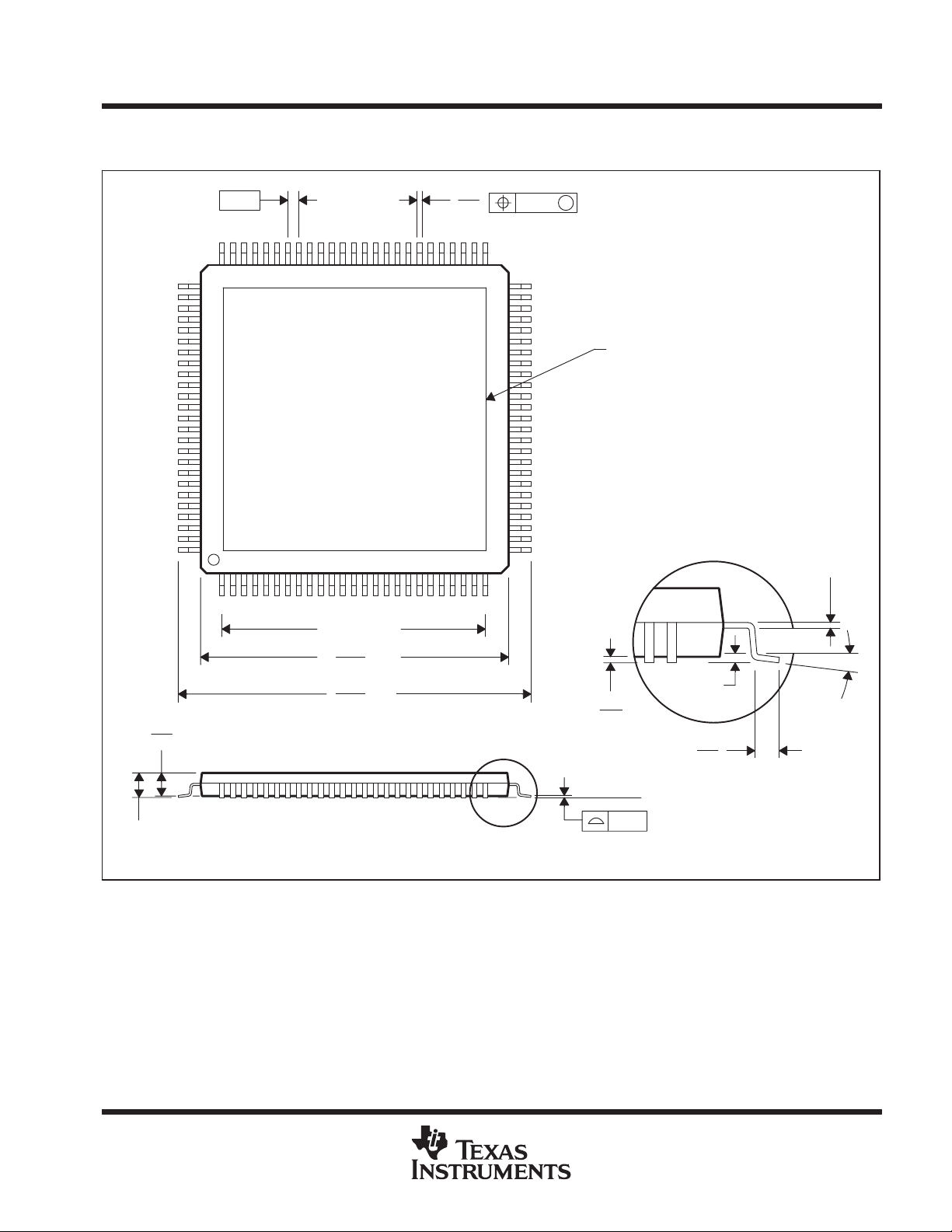
MECHANICAL DATA
PFD (S-PQFP-G100) PowerPAD PLASTIC QUAD FLATPACK (DIE DOWN)
76
100
1,05
0,95
75
1
0,50
12,00 TYP
14,20
SQ
13,80
16,20
SQ
15,80
0,27
0,17
25
51
0,08
50
26
M
Thermal Pad
(see Note D)
0,13 NOM
Gage Plane
0,25
0,15
0,05
0,75
0,45
0°–7°
1,20 MAX
NOTES: A. All linear dimensions are in millimeters.
B. This drawing is subject to change without notice.
C. Body dimensions do not include mold flash or protrusion.
D. The package thermal performance may be enhanced by attaching an external heatsink to the thermal pad.
This pad is electrically and thermally connected to the backside of the die and possibly selected leads.
E. Falls within JEDEC MS-026
PowerPAD is a trademark of Texas Instruments Incorporated.
POST OFFICE BOX 655303 • DALLAS, TEXAS 75265
Seating Plane
0,08
4146930/A 12/97
11

IMPORTANT NOTICE
T exas Instruments and its subsidiaries (TI) reserve the right to make changes to their products or to discontinue
any product or service without notice, and advise customers to obtain the latest version of relevant information
to verify, before placing orders, that information being relied on is current and complete. All products are sold
subject to the terms and conditions of sale supplied at the time of order acknowledgement, including those
pertaining to warranty, patent infringement, and limitation of liability.
TI warrants performance of its semiconductor products to the specifications applicable at the time of sale in
accordance with TI’s standard warranty. Testing and other quality control techniques are utilized to the extent
TI deems necessary to support this warranty . Specific testing of all parameters of each device is not necessarily
performed, except those mandated by government requirements.
CERTAIN APPLICA TIONS USING SEMICONDUCTOR PRODUCTS MA Y INVOLVE POTENTIAL RISKS OF
DEATH, PERSONAL INJURY, OR SEVERE PROPERTY OR ENVIRONMENTAL DAMAGE (“CRITICAL
APPLICATIONS”). TI SEMICONDUCTOR PRODUCTS ARE NOT DESIGNED, AUTHORIZED, OR
WARRANTED TO BE SUITABLE FOR USE IN LIFE-SUPPORT DEVICES OR SYSTEMS OR OTHER
CRITICAL APPLICA TIONS. INCLUSION OF TI PRODUCTS IN SUCH APPLICATIONS IS UNDERST OOD TO
BE FULLY AT THE CUSTOMER’S RISK.
In order to minimize risks associated with the customer’s applications, adequate design and operating
safeguards must be provided by the customer to minimize inherent or procedural hazards.
TI assumes no liability for applications assistance or customer product design. TI does not warrant or represent
that any license, either express or implied, is granted under any patent right, copyright, mask work right, or other
intellectual property right of TI covering or relating to any combination, machine, or process in which such
semiconductor products or services might be or are used. TI’s publication of information regarding any third
party’s products or services does not constitute TI’s approval, warranty or endorsement thereof.
Copyright 2000, Texas Instruments Incorporated
 Loading...