


SN75LVDS84A
FLATLINK TRANSMITTER
SLLS354C – MAY 1999 – REVISED NOVEMBER 1999
D
21:3 Data Channel Compression at up to
196 Million Bytes per Second Throughput
D
Suited for SVGA, XGA, or SXGA Data
Transmission From Controller to Display
With Very Low EMI
D
21 Data Channels Plus Clock In
Low-Voltage TTL inputs and 3 Data
Channels Plus Clock Out Low-Voltage
Differential Signaling (LVDS) Outputs
D
Operates From a Single 3.3-V Supply and
89 mW (Typ)
D
Ultra Low Power 3.3-V CMOS Version of the
SN75LVDS84. Power Consumption About
One Third of the ’LVDS84
D
Packaged in Thin Shrink Small-Outline
Package (TSSOP) With 20 Mil Terminal
Pitch
D
Consumes Less Than 0.54 mW When
Disabled
D
Wide Phase-Lock Input Frequency Range:
31 MHz to 75 MHz
D
No External Components Required for PLL
D
Outputs Meet or Exceed the Requirements
of ANSI EIA/TIA–644 Standard
D
SSC Tracking Capability of 3% Center
Spread at 50-kHz Modulation Frequency
D
Improved Replacement for SN75LVDS84
and NSC’s DS90CF363A 3-V Device
description
DGG PACKAGE
(TOP VIEW)
D4
1
48
V
GND
V
GND
GND
V
GND
NC – Not Connected
CC
D5
D6
D7
D8
CC
D9
D10
D11
D12
NC
D13
D14
D15
D16
D17
CC
D18
D19
2
3
4
5
6
7
8
9
10
11
12
13
14
15
16
17
18
19
20
21
22
23
24
47
46
45
44
43
42
41
40
39
38
37
36
35
34
33
32
31
30
29
28
27
26
25
D3
D2
GND
D1
D0
NC
LVDSGND
Y0M
Y0P
Y1M
Y1P
LVDSV
CC
LVDSGND
Y2M
Y2P
CLKOUTM
CLKOUTP
LVDSGND
PLLGND
PLLV
CC
PLLGND
SHTDN
CLKIN
D20
The SN75LVDS84A FlatLink transmitter contains three 7-bit parallel-load serial-out shift registers, and four
low-voltage differential signaling (L VDS) line drivers in a single integrated circuit. These functions allow 21 bits
of single-ended L VTTL data to be synchronously transmitted over 3 balanced-pair conductors for receipt by a
compatible receiver, such as the SN75LVDS82 or SN75LVDS86/86A.
When transmitting, data bits D0 – D20 are each loaded into registers of the ’LVDS84A upon the falling edge.
The internal PLL is frequency-locked to CLKIN and then used to unload the data registers in 7-bit slices. The
three serial streams and a phase-locked clock (CLKOUT) are then output to L VDS output drivers. The frequency
of CLKOUT is the same as the input clock, CLKIN.
The ’L VDS84A requires no external components and little or no control. The data bus appears the same at the
input to the transmitter and output of the receiver with the data transmission transparent to the user(s). The only
user intervention is the possible use of the shutdown/clear (SHTDN
) active-low input to inhibit the clock and shut
off the L VDS output drivers for lower power consumption. A low-level on this signal clears all internal registers
to a low level.
The SN75LVDS84A is characterized for operation over ambient free-air temperatures of 0_C to 70_C.
Please be aware that an important notice concerning availability, standard warranty, and use in critical applications of
Texas Instruments semiconductor products and disclaimers thereto appears at the end of this data sheet.
FlatLink is a trademark of Texas Instruments Incorporated.
PRODUCTION DATA information is current as of publication date.
Products conform to specifications per the terms of Texas Instruments
standard warranty. Production processing does not necessarily include
testing of all parameters.
POST OFFICE BOX 655303 • DALLAS, TEXAS 75265
Copyright 1999, Texas Instruments Incorporated
1

SN75LVDS84A
FLATLINK TRANSMITTER
SLLS354C – MAY 1999 – REVISED NOVEMBER 1999
functional block diagram
D0 – D6
D7 – D13
D14 – D20
7
7
7
Parallel-Load 7-Bit
Shift Register
A,B, ...G
SHIFT/LOAD
CLK
Parallel-Load 7-Bit
Shift Register
A,B, ...G
SHIFT/LOAD
CLK
Parallel-Load 7-Bit
Shift Register
A,B, ...G
SHIFT/LOAD
CLK
Y0P
Y0M
Y1P
Y1M
Y2P
Y2M
SHTDN
CLKIN
schematics of input and output
EQUIVALENT OF EACH INPUT EQUIVALENT OF EACH OUTPUT
7 V
D or
SHTDN
180 Ω
5 V
Control Logic
PLL
CLK
CLKINH
V
V
CC
CC
CLKOUTP
CLKOUTM
YnP or YnM
7 V
2
POST OFFICE BOX 655303 • DALLAS, TEXAS 75265
SN75LVDS84A
FLATLINK TRANSMITTER
SLLS354C – MAY 1999 – REVISED NOVEMBER 1999
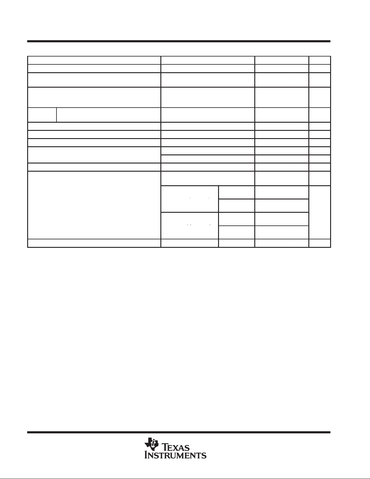
absolute maximum ratings over operating free-air temperature (unless otherwise noted)
†
Supply voltage range, VCC (see Note 1) –0.5 V to 4 V. . . . . . . . . . . . . . . . . . . . . . . . . . . . . . . . . . . . . . . . . . . . . . . . . . . .
Input and output voltage ranges, VI, VO (all terminals) –0.5 V to V
CC
+ 0.5 V. . . . . . . . . . . . . . . . . . . . . . . . . . . .
Continuous total power dissipation See Dissipation Rating Table. . . . . . . . . . . . . . . . . . . . . . . . . . . . . . . . . . . . . .
Electrostatic discharge: ESD machine model 200 V. . . . . . . . . . . . . . . . . . . . . . . . . . . . . . . . . . . . . . . . . . . . . . . . .
ESD human-body model 6000 V. . . . . . . . . . . . . . . . . . . . . . . . . . . . . . . . . . . . . . . . . . . . .
ESD charged-device model 1500 V. . . . . . . . . . . . . . . . . . . . . . . . . . . . . . . . . . . . . . . . . .
Storage temperature range, T
stg
–65_C to 150_C. . . . . . . . . . . . . . . . . . . . . . . . . . . . . . . . . . . . . . . . . . . . . . . . . . .
Lead temperature 1,6 mm (1/16 inch) from case for 10 seconds 260_C. . . . . . . . . . . . . . . . . . . . . . . . . . . . . . . .
†
Stresses beyond those listed under “absolute maximum ratings” may cause permanent damage to the device. These are stress ratings only, and
functional operation of the device at these or any other conditions beyond those indicated under “recommended operating conditions” is not
implied. Exposure to absolute-maximum-rated conditions for extended periods may affect device reliability.
NOTE 1: All voltage values are with respect to the GND terminals.
DISSIPATION RATING TABLE
PACKAGE
DGG 1316 mW 13.1 mW/°C 726 mW
‡
This is the inverse of the junction-to-ambient thermal resistance when board mounted and
with no air flow.
TA ≤ 25°C
POWER RATING
DERATING FACTOR
ABOVE TA = 25°C
‡
POWER RATING
TA = 70°C
recommended operating conditions
MIN NOM MAX UNIT
Supply voltage, V
High-level input voltage, V
Low-level input voltage, V
Differential load impedance, Z
Operating free-air temperature, T
CC
IH
IL
L
A
3 3.3 3.6 V
2 V
0.8 V
90 132 Ω
0 70 °C
timing requirements
MIN NOM MAX UNIT
t
Input clock period 13.3 tc32.4 ns
c
t
Pulse duration, high-level input clock 0.4t
w
t
Transition time, input signal 5 ns
t
t
Setup time, data, D0 – D20 valid before CLKIN↓ (See Figure 2) 3 ns
su
t
Hold time, data, D0 – D20 valid after CLKIN↓ (See Figure 2) 1.5 ns
h
c
0.6t
ns
c
POST OFFICE BOX 655303 • DALLAS, TEXAS 75265
3
SN75LVDS84A
IOSShort-circuit output current
)
L
()
)
mA
L
,( )
FLATLINK TRANSMITTER
SLLS354C – MAY 1999 – REVISED NOVEMBER 1999
electrical characteristics over recommended operating conditions (unless otherwise noted)
PARAMETER TEST CONDITIONS MIN TYP†MAX UNIT
V
IT
|VOD|
∆|VOD|
V
OC(SS)
V
OC(PP)
I
IH
I
IL
I
OZ
I
CC(AVG)
C
I
†
All typical values are at VCC = 3.3 V, TA = 25°C.
Input threshold voltage 1.4 V
Differential steady-state output voltage magni-
tude
Change in the steady-state differential output
voltage magnitude between opposite binary
states
Steady-state common-mode output voltage
Peak-to-peak common-mode output voltage 80 150 mV
High-level input current VIH = V
Low-level input current VIL = 0 ±10 µA
p
High-impedance output current VO = 0 to V
Quiescent supply current (average)
Input capacitance 2 pF
RL = 100 Ω,
See Figure 3
RL = 100 Ω,
See Figure 3
CC
V
= 0 –6 ±24 mA
O(Yn)
VOD = 0 –6 ±12 mA
CC
Disabled,
All inputs at GND
Enabled,
R
= 100 Ω (4 places
Gray-scale pattern
(see Figure 4)
Enabled,
R
= 100 Ω, (4 places
Worst-case pattern
(see Figure 5)
f = 65 MHz 27 35
f = 75 MHz 30 38
f = 65 MHz 28 36
f = 75 MHz 31 39
247 454 mV
50 mV
1.125 1.375 V
20 µA
±10 µA
15 150 µA
4
POST OFFICE BOX 655303 • DALLAS, TEXAS 75265
See Figure 6
∆t
Cycl
§
SN75LVDS84A
FLATLINK TRANSMITTER
SLLS354C – MAY 1999 – REVISED NOVEMBER 1999
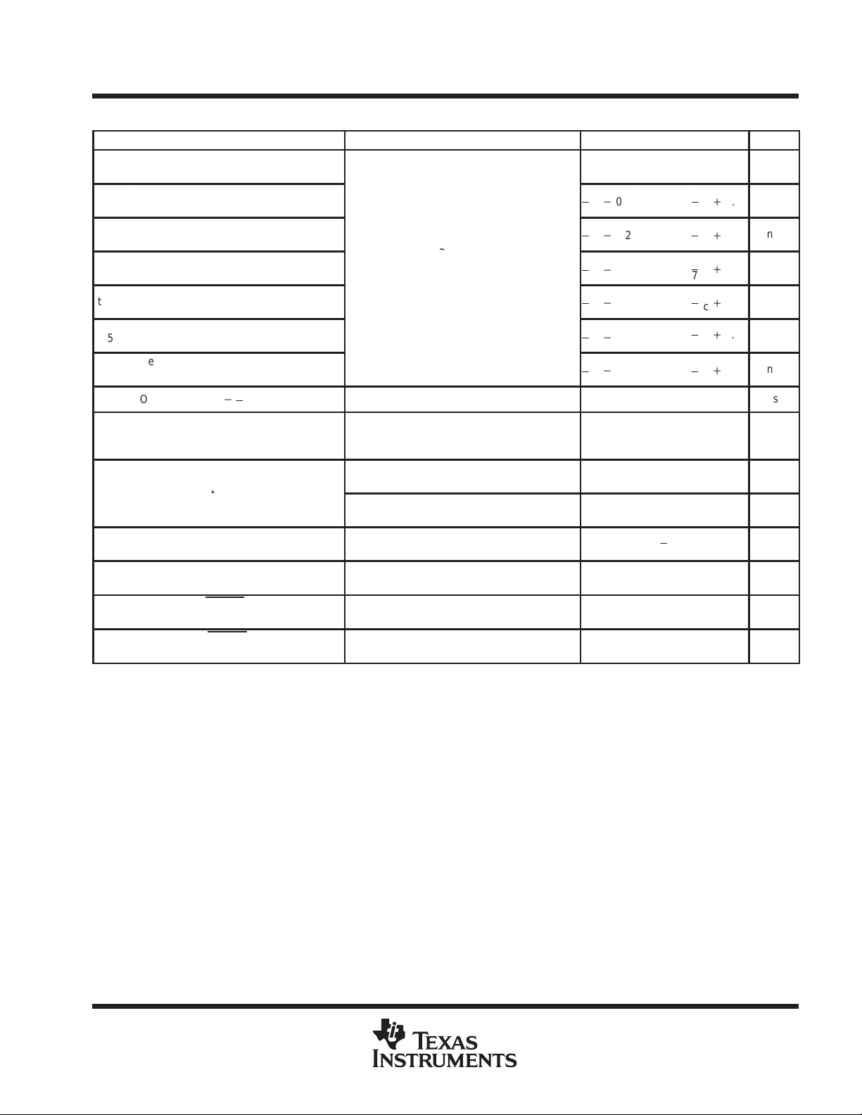
switching characteristics over recommended operating conditions (unless otherwise noted)
PARAMETER TEST CONDITIONS MIN TYP
Delay time, CLKOUT↑ to serial bit
t
d0
position 0
Delay time, CLKOUT↑ to serial bit
t
d1
position 1
Delay time, CLKOUT↑ to serial bit
t
d2
position 2
Delay time, CLKOUT↑ to serial bit
t
d3
position 3
Delay time, CLKOUT↑ to serial bit
t
d4
position 4
Delay time, CLKOUT↑ to serial bit
t
d5
position 5
Delay time, CLKOUT↑ to serial bit
t
d6
position 6
t
Output skew,
sk(o)
t
Delay time, CLKIN↓ to CLKOUT↑
d7
c(o)
t
w
t
t
t
en
t
dis
†
All typical values are at VCC = 3.3 V, TA = 25°C.
‡
|Input clock jitter| is the magnitude of the change in the input clock period.
§
Output clock jitter is the change in the output clock period from one cycle to the next cycle observed over 15000 cycles.
e time, output clock jitter
Pulse duration, high-level output clock
Transition time, differential output
voltage (tr or tf)
Enable time, SHTDN↑ to phase lock
(Yn valid)
Disable time, SHTDN↓ to off state
(CLKOUT low)
tn*
n
t
c
7
tc = 15.38 ns (± 0.2%),
|Input clock jitter| < 50 ps‡,
tc = 15.38 ns (± 0.2%),
|Input clock jitter| < 50 ps‡,
See Figure 6
tc = 15.38 + 0.308 sin (2π500E3t) ± 0.05 ns,
See Figure 7
tc = 15.38 + 0.308 sin (2π3E6t) ± 0.05 ns,
See Figure 7
See Figure 3 700 1500 ps
See Figure 8 1 ms
See Figure 9 6.5 ns
–0.2 0.2 ns
1
tc*
0.2
7
2
tc*
0.2
7
3
tc*
0.2
7
4
tc*
0.2
7
5
tc*
0.2
7
6
tc*
0.2
7
–0.2 0.2 ns
†
2.7 ns
±62 ps
±121 ps
4
t
c
7
MAX UNIT
1
tc)
7
2
tc)
7
3
tc)
7
4
tc)
7
5
tc)
7
6
tc)
7
0.2
0.2
0.2
0.2
0.2
0.2
ns
ns
ns
ns
ns
ns
ns
POST OFFICE BOX 655303 • DALLAS, TEXAS 75265
5
 Loading...