

swivel
SN75LVDS83B
FlatLink Transmitter
TM
PackageOptions
TSSOP:8x14mmDGG
BGA:4.5x7mm
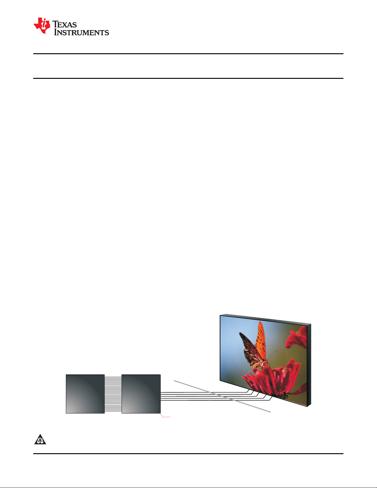
Application
processor
(e.g.OMAP )
TM
SN75LVDS83B
www.ti.com
FLATLINK™ TRANSMITTER
Check for Samples: SN75LVDS83B
1
FEATURES
2
• LVDS Display Serdes Interfaces Directly to
LCD Display Panels with Integrated LVDS
• Package Options: 4.5mm x 7mm BGA, and
8.1mm x 14mm TSSOP
• 1.8V up to 3.3V Tolerant Data Inputs to
Connect Directly to Low-Power, Low-Voltage
Application and Graphic Processors
• Transfer Rate up to 135Mpps (Mega Pixel Per
Second); Pixel Clock Frequency Range 10MHz
to 135MHz
• Suited for Display Resolutions Ranging From
HVGA up to HD With Low EMI
• Operates From a Single 3.3V Supply and
170mW (typ.) at 75MHz
• 28 Data Channels Plus Clock In Low-Voltage
TTL to 4 Data Channels Plus Clock Out Low-
SLLS846B –MAY 2009–REVISED SEPTEMBER 2011
Voltage Differential
• Consumes Less Than 1mW When Disabled
• Selectable Rising or Falling Clock Edge
Triggered Inputs
• ESD: 5kV HBM
• Support Spread Spectrum Clocking (SSC)
• Compatible with all OMAP™2x, OMAP™3x,
and DaVinci™ Application Processors
APPLICATIONS
• LCD Display Panel Driver
• UMPC and Netbook PC
• Digital Picture Frame
DESCRIPTION
The SN75LVDS83B FlatLink™ transmitter contains four 7-bit parallel-load serial-out shift registers, a 7X clock
synthesizer, and five Low-Voltage Differential Signaling (LVDS) line drivers in a single integrated circuit. These
functions allow 28 bits of single-ended LVTTL data to be synchronously transmitted over five balanced-pair
conductors for receipt by a compatible receiver, such as the SN75LVDS82 and LCD panels with integrated LVDS
receiver.
When transmitting, data bits D0 through D27 are each loaded into registers upon the edge of the input clock
signal (CLKIN). The rising or falling edge of the clock can be selected via the clock select (CLKSEL) pin. The
frequency of CLKIN is multiplied seven times, and then used to unload the data registers in 7-bit slices and
serially. The four serial streams and a phase-locked clock (CLKOUT) are then output to LVDS output drivers.
The frequency of CLKOUT is the same as the input clock, CLKIN.
1
Please be aware that an important notice concerning availability, standard warranty, and use in critical applications of
Texas Instruments semiconductor products and disclaimers thereto appears at the end of this data sheet.
2OMAP, DaVinci, FlatLink are trademarks of Texas Instruments.
PRODUCTION DATA information is current as of publication date.
Products conform to specifications per the terms of the Texas
Instruments standard warranty. Production processing does not
necessarily include testing of all parameters.
Copyright © 2009–2011, Texas Instruments Incorporated

SN75LVDS83B
SLLS846B –MAY 2009–REVISED SEPTEMBER 2011
This integrated circuit can be damaged by ESD. Texas Instruments recommends that all integrated circuits be handled with
appropriate precautions. Failure to observe proper handling and installation procedures can cause damage.
ESD damage can range from subtle performance degradation to complete device failure. Precision integrated circuits may be more
susceptible to damage because very small parametric changes could cause the device not to meet its published specifications.
www.ti.com
DESCRIPTION (CONTINUED)
The SN75LVDS83B requires no external components and little or no control. The data bus appears the same at
the input to the transmitter and output of the receiver with the data transmission transparent to the user(s). The
only user intervention is selecting a clock rising edge by inputting a high level to CLKSEL or a falling edge with a
low-level input, and the possible use of the Shutdown/Clear (SHTDN). SHTDN is an active-low input to inhibit the
clock, and shut off the LVDS output drivers for lower power consumption. A low-level on this signal clears all
internal registers to a low-level.
The SN75LVDS83B is characterized for operation over ambient air temperatures of -10°C to 70°C.
Alternative device option: The SN75LVDS83A (SLLS980) is an alternative to the SN75LVDS83B for clock
frequency range of 10MHz-100MHz only. The SN75LVDS83A is available in the TSSOP package option only.
ORDERING INFORMATION
PART NUMBER PART MARKING PACKAGE
SN75LVDS83BZQLR LVDS83B in BGA package 56-pin ZQL LARGE T&R
SN75LVDS83BDGG LVDS83B in TSSOP package 56-pin DGG TUBE
SN75LVDS83BDGGR LVDS83B in TSSOP package 56-pin DGG LARGE T&R
(1) For the most current package and ordering information, see the Package Option Addendum located at the end of this data sheet, or
refer to our web site at www.ti.com.
(1)
ABSOLUTE MAXIMUM RATINGS
Supply voltage range, VCC, IOVCC, LVDSVCC, PLLVCC
Voltage range at any output terminal -0.5 to VCC + 0.5 V
Voltage range at any input terminal -0.5 to IOVCC + 0.5 V
Continuous power dissipation See the dissipation rating table
Storage temperature, T
ESD rating Charged Device Model (CDM)
(1) Stresses above these ratings may cause permanent damage. Exposure to absolute maximum conditions for extended periods may
degrade device reliability. These are stress ratings only, and functional operation of the device at these or any other conditions beyond
those specified is not implied.
(2) All voltages are with respect to the GND terminals.
(3) In accordance with JEDEC Standard 22, Test Method A114-A.
(4) In accordance with JEDEC Standard 22, Test Method C101.
(5) In accordance with JEDEC Standard 22, Test Method A115-A.
s
Human Body Model (HBM)
Machine Model (MM)
(5)
(1)
VALUE UNIT
(2)
(3)
all pins 5 kV
(4)
all pins 500 V
all pins 150 V
-0.5 to 4 V
–65 to 150 °C
2 Copyright © 2009–2011, Texas Instruments Incorporated
SN75LVDS83B
www.ti.com
SLLS846B –MAY 2009–REVISED SEPTEMBER 2011
RECOMMENDED OPERATING CONDITIONS
over operating free-air temperature range (unless otherwise noted)
PARAMETER MIN NOM MAX UNIT
Supply voltage, VCC 3 3.3 3.6
LVDS output Supply voltage, LVDSVCC 3 3.3 3.6
PLL analog supply voltage, PLLVCC 3 3.3 3.6 V
IO input reference supply voltage, IOVCC 1.62 1.8 / 2.5 / 3.3 3.6
Power supply noise on any VCC terminal 0.1
IOVCC = 1.8V IOVCC/2 + 0.3V
High-level input voltage, V
Low-level input voltage, V
Differential load impedance, Z
IH
IL
L
Operating free-air temperature, T
A
IOVCC = 2.5V IOVCC/2 + 0.4V V
IOVCC = 3.3V IOVCC/2 + 0.5V
IOVCC = 1.8V IOVCC/2 - 0.3V
IOVCC = 2.5V IOVCC/2 - 0.4V V
IOVCC = 3.3V IOVCC/2 - 0.5V
90 132 Ω
-10 70 C
DISSIPATION RATINGS
PACKAGE CIRCUIT BOARD MODEL
DGG 1111mW 12.3mW/°C 555mW
ZQL 1034mW 11.5mW/°C 517mW
(3)
DGG
ZQL 2000mW 22mW/°C 1000mW
Low-K
High-K
(1)
TJA≤ 25°C
1730mW 19mW/°C 865mW
DERATING FACTOR
ABOVE TJA= 25°C POWER RATING
(1) In accordance with the High-K and Low-K thermal metric definitions of EIA/JESD51-2.
(2) This is the inverse of the junction-to-ambient thermal resistance when board-mounted and with no air flow.
(3) DGG junction to case thermal reistance (θJC) is 15.4°C/W.
(2)
TJA= 70°C
TIMING REQUIREMENTS
PARAMETER MIN MAX UNIT
Input clock period, t
Input clock modulation
High-level input clock pulse width duration, t
Input signal transition time, t
c
with modulation frequency 30kHz 8%
with modulation frequency 50kHz 6%
w
t
Data set up time, D0 through D27 before CLKIN (See Figure 3) 2 ns
Data hold time, D0 through D27 after CLKIN 0.8 ns
7.4 100 ns
0.4 t
c
0.6 t
c
3 ns
ns
Copyright © 2009–2011, Texas Instruments Incorporated 3
1
2
3
4
5
6
7
8
9
10
11
12
13
14
15
16
17
18
19
20
21
22
23
24
25
26
27
28 29
30
31
32
33
34
35
36
37
38
39
40
41
42
43
44
45
46
47
48
49
50
51
52
53
54
55
56
IOVCC
VCC
LVDSVCC
GND
CLKSEL
D16
D15
D14
GND
CLKOUTM
D13
D17
D5
D6
D7
D8
D10
D11
D18
GND
D21
D23
D24
D2
D3
D4
GND
D1
D0
D27
GND
Y0M
GND
GND
PLLVCC
GND
SHTDN
CLKIN
D26
GND
GND
D9
D12
D19
D20
D22
IOVCC
D25
Y0P
Y1M
Y1P
Y2M
Y2P
Y3M
Y3P
CLKOUTP
SN75LVDS83B
SLLS846B –MAY 2009–REVISED SEPTEMBER 2011
www.ti.com
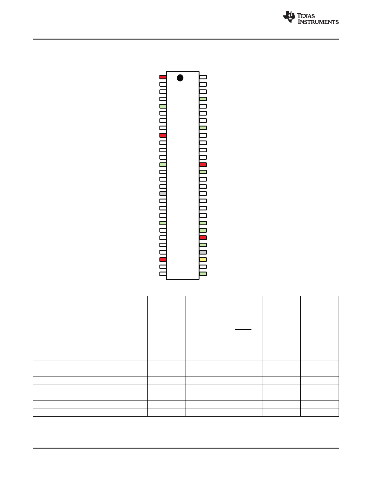
DGG PACKAGE
(TOP VIEW)
4 Copyright © 2009–2011, Texas Instruments Incorporated
Pin # Signal Pin # Signal Pin # Signal Pin # Signal
1 IOVCC 15 D15 29 GND 43 GND
2 D5 16 D16 30 D26 44 LVDSVCC
3 D6 17 CLKSEL 31 CLKIN 45 Y1P
4 D7 18 D17 32 SHTDN 46 Y1M
5 GND 19 D18 33 GND 47 Y0P
6 D8 20 D19 34 PLLVCC 48 Y0M
7 D9 21 GND 35 GND 49 GND
8 D10 22 D20 36 GND 50 D27
9 VCC 23 D21 37 Y3P 51 D0
10 D11 24 D22 38 Y3M 52 D1
11 D12 25 D23 39 CLKOUTP 53 GND
12 D13 26 IOVCC 40 CLKOUTM 54 D2
13 GND 27 D24 41 Y2P 55 D3
14 D14 28 D25 42 Y2M 56 D4
DGG PIN LIST
13 2456
K
G
H
J
D
E
F
C
D13
D14
D16
D17
GND Y3M
D15
GND
GND
GND
Y1P
Y2P
LVDSVCC
Y1M
Y2M
GND
Y0M
CLKM
CLKSEL
D8
CLKP
Y0P
D12
D11
D19
D3
D1
D27D6
D7
GND
D4D5
D0
D2
Y3P
D18
B
A
D22
D20
D26
GND
GNDD24
D21
D23
SHTDND25
CLKIN
PLLVCC
IOVCC
IOVCC
VCC
GND
GND
D10
D9
SN75LVDS83B
www.ti.com
SLLS846B –MAY 2009–REVISED SEPTEMBER 2011
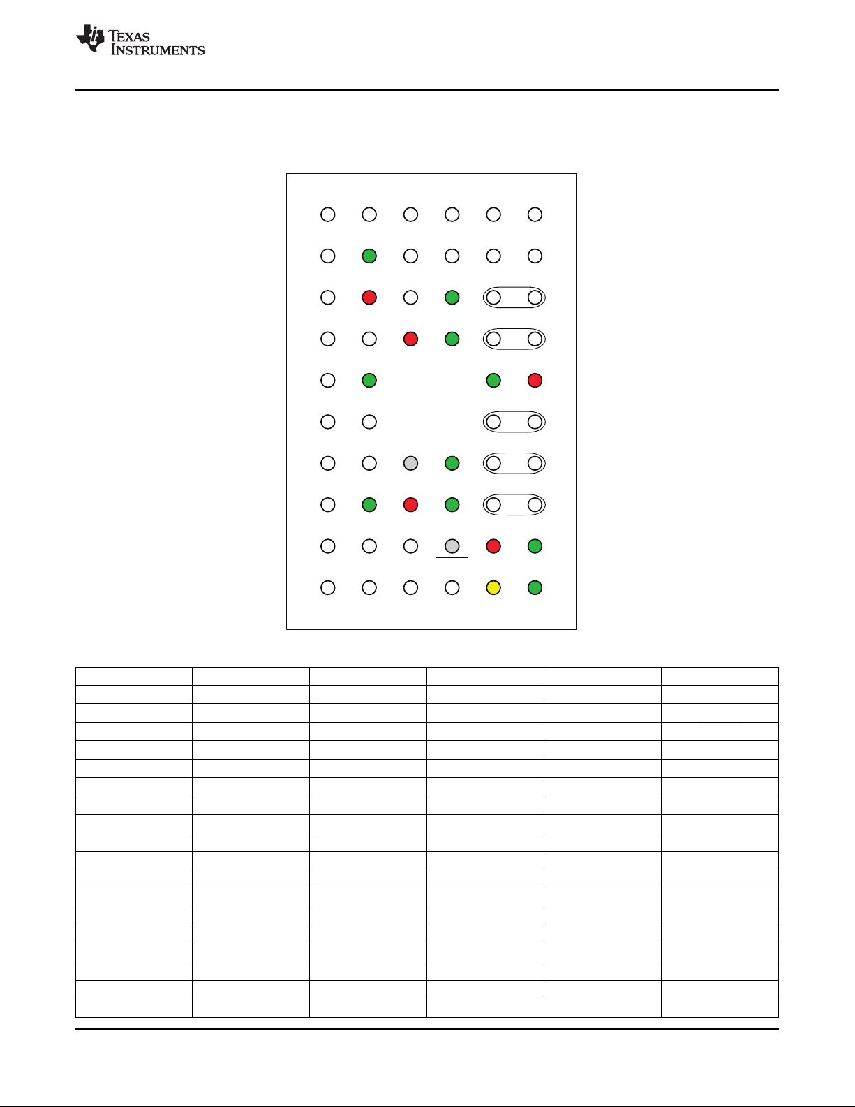
ZQL PACKAGE
(TOP VIEW)
ZQL PIN LIST
Copyright © 2009–2011, Texas Instruments Incorporated 5
Ball # Signal Ball # Signal Ball # Signal
A1 GND A2 CLKIN A3 D26
A4 D24 A5 D23 A6 D22
B1 GND B2 PLLVCC B3 SHTDN
B4 D25 B5 D21 B6 D20
C1 Y3M C2 Y3P C3 GND
C4 IOVCC C5 GND C6 D19
D1 CLKM D2 CLKP D3 GND
D4 CLKSEL D5 D18 D6 D17
E1 Y2M E2 Y2P E3 ball not populated
E4 ball not populated E5 D15 E6 D16
F1 LVDSVCC F2 GND F3 ball not populated
F4 ball not populated F5 GND F6 D14
G1 Y1M G2 Y1P G3 GND
G4 IOVCC G5 D12 G6 D13
H1 Y0M H2 Y0P H3 GND
H4 D10 H5 VCC H6 D11
J1 D27 J2 D0 J3 D3
J4 D6 J5 GND J6 D9
SN75LVDS83B
SLLS846B –MAY 2009–REVISED SEPTEMBER 2011
www.ti.com
ZQL PIN LIST (continued)
K1 D1 K2 D2 K3 D4
K4 D5 K5 D7 K6 D8
PIN FUNCTIONS
TERMINAL I/O DESCRIPTION
Y0P, Y0M, Y1P, Differential LVDS data outputs.
Y1M, Y2P, Y2M Outputs are high-impedance when SHTDN is pulled low (de-asserted)
Y3P, Y3M LVDS Out Output is high-impedance when SHTDN is pulled low (de-asserted).
CLKP, CLKM
D0 – D27
CMOS IN with
CLKIN Input pixel clock; rising or falling clock polarity is selectable by Control input CLKSEL.
SHTDN
CLKSEL
VCC 3.3V digital supply voltage
IOVCC I/O supply reference voltage (1.8V up to 3.3V matching the GPU data output signal swing)
PLLVCC Power Supply
LVDSVCC 3.3V LVDS output analog supply
GND Supply ground for VCC, IOVCC, LVDSVCC, and PLLVCC.
(1) For a multilayer pcb, it is recommended to keep one common GND layer underneath the device and connect all ground terminals
directly to this plane.
pulldn
Differential LVDS Data outputs.
Note: if the application only requires 18-bit color, this output can be left open.
Differential LVDS pixel clock output.
Output is high-impedance when SHTDN is pulled low (de-asserted).
Data inputs; supports 1.8V to 3.3V input voltage selectable by VDD supply. To connect a graphic
source successfully to a display, the bit assignment of D[27:0] is critical (and not necessarily
intuitive).
For input bit assignment see Figure 14 to Figure 17 for details.
Note: if application only requires 18-bit color, connect unused inputs D5, D10, D11, D16, D17, D23,
and D27 to GND.
Device shut down; pull low (de-assert) to shut down the device (low power, resets all registers) and
high (assert) for normal operation.
Selects between rising edge input clock trigger (CLKSEL = VIH) and falling edge input clock trigger
(CLKSEL = VIL).
(1)
3.3V PLL analog supply
6 Copyright © 2009–2011, Texas Instruments Incorporated
Parallel-Load7-bit
ShiftRegister
A,B,...G
SHIFT/LOAD
>CLK
7D0,D1,D2,D3,
D4,D6,D7
Y0P
Y0M
Parallel-Load7-bit
ShiftRegister
A,B,...G
SHIFT/LOAD
>CLK
7D8,D9,D12,D13,
D14,D15,D18
Y1P
Y1M
Parallel-Load7-bit
ShiftRegister
A,B,...G
SHIFT/LOAD
>CLK
7D19,D20,D21,D22,
D24,D25,D26
Y2P
Y2M
7XClock/PLL
7XCLK
>CLK
CLKINH
RISING/FALLINGEDGE
CLKIN
CLKOUTP
CLKOUTM
SHTDN
Parallel-Load7-bit
ShiftRegister
A,B,...G
SHIFT/LOAD
>CLK
7D27,D5,D10,D11,
D16, D17,D23
Y3P
Y3M
ControlLogic
CLKSEL
SN75LVDS83B
www.ti.com
SLLS846B –MAY 2009–REVISED SEPTEMBER 2011
FUNCTIONAL BLOCK DIAGRAM
Copyright © 2009–2011, Texas Instruments Incorporated 7
D0-1
D8-1
D19-1
D27-1
D7
D18
D26
D23 D17
D25
D15
D6
D16
D24
D14
D4
D11
D22
D13
D3
D10
D21
D12
D2
D5
D20
D9
D1
D27
D19
D8
D0
D23+1
D26+1
D18+1
D7+1
Dn
CLKIN
CLKOUT
Y0
Y1
Y2
Y3
Previouscycle
Currentcycle
Next
CLKIN
or
7V
Dor
IOVCC
LVDSVCC
SHTDN
50W
7V
5W
YnP or
YnM
10kW
300kW
SN75LVDS83B
SLLS846B –MAY 2009–REVISED SEPTEMBER 2011
Figure 1. Typical SN75LVDS83B Load and Shift Sequences
www.ti.com
Figure 2. Equivalent Input and Output Schematic Diagrams
8 Copyright © 2009–2011, Texas Instruments Incorporated
SN75LVDS83B
www.ti.com
SLLS846B –MAY 2009–REVISED SEPTEMBER 2011
ELECTRICAL CHARACTERISTICS
over operating free-air temperature range (unless otherwise noted)
PARAMETER TEST CONDITIONS MIN TYP
V
T
|VOD| 250 450
Δ|VOD| output voltage magnitude between 1 35 mV
V
OC(SS)
V
OC(PP)
I
IH
I
IL
I
OS
I
OZ
R
pdn
I
Q
I
CC
C
I
(1) All typical values are at VCC = 3.3V, TA= 25°C.
Input voltage threshold IOVCC/2 V
Differential steady-state output voltage mV
magnitude
RL= 100Ω, See Figure 4
Change in the steady-state differential
opposite binary states
Steady-state common-mode output
voltage
Peak-to-peak common-mode output
See Figure 4
t
(Dx, CLKin) = 1ns
R/F
1.125 1.375 V
voltage
High-level input current VIH= IOVCC 25 μA
Low-level input current VIL= 0 V ±10 μA
Short-circuit output current
VOY= 0 V ±24 mA
VOD= 0 V ±12 mA
High-impedance state output current VO= 0 V to VCC ±20 μA
Input pull-down integrated resistor on all
inputs (Dx, CLKSEL, SHTDN, CLKIN)
Quiescent current (average) 2 100 μA
IOVCC = 1.8V 200
IOVCC = 3.3V 100
disabled, all inputs at GND;
SHTDN = V
IL
SHTDN = VIH, RL= 100Ω (5 places),
grayscale pattern (Figure 5)
VCC = 3.3V, f
CLK
= 75MHz
I
(VCC)
I
(IOVCC)
I
(IOVCC)
+ I
+ I
(PLLVCC)
(LVDSVCC)
with IOVCC = 3.3V 0.4 mA
with IOVCC = 1.8V 0.1
SHTDN = VIH, RL= 100Ω (5 places), 50%
transition density pattern (Figure 5),
VCC = 3.3V, f
CLK
= 75MHz
I
(VCC)
I
(IOVCC)
I
(IOVCC)
+ I
+ I
(PLLVCC)
(LVDSVCC)
with IOVCC = 3.3V 0.6 mA
with IOVCC = 1.8V 0.2
SHTDN = VIH, RL= 100Ω (5 places), worstcase pattern (Figure 6),
VCC = 3.6V, f
Supply current (average)
CLK
= 75MHz
I
(VCC)
I
(IOVCC)
I
(IOVCC)
+ I
+ I
(PLLVCC)
(LVDSVCC)
with IOVCC = 3.3V 1.3 mA
with IOVCC = 1.8V 0.5
SHTDN = VIH, RL= 100Ω (5 places), worstcase pattern (Figure 6),
f
= 100MHz
CLK
I
(VCC)
I
(IOVCC)
I
(IOVCC)
+ I
+ I
(PLLVCC)
(LVDSVCC)
with IOVCC = 3.6V 1.6 mA
with IOVCC = 1.8V 0.6
SHTDN = VIH, RL= 100Ω (5 places), worstcase pattern (Figure 6),
f
= 135MHz
CLK
I
(VCC)
I
(IOVCC)
I
(IOVCC)
+ I
+ I
(PLLVCC)
(LVDSVCC)
with IOVCC = 3.6V 2.1 mA
with IOVCC = 1.8V 0.8
Input capacitance 2 pF
51.9
53.3
63.7
81.6
102.2
(1)
MAX UNIT
35 mV
kΩ
Copyright © 2009–2011, Texas Instruments Incorporated 9
SN75LVDS83B
SLLS846B –MAY 2009–REVISED SEPTEMBER 2011
www.ti.com
SWITCHING CHARACTERISTICS
over operating free-air temperature range (unless otherwise noted)
4
±26
±44
±35
±42
/7t
(1)
1
2
3
4
5
6
c
c
MAX UNIT
/7tc+ 0.1 ns
/7tc+ 0.1 ns
/7tc+ 0.1 ns
/7tc+ 0.1 ns
/7tc+ 0.1 ns
/7tc+ 0.1 ns
ns
ps
ns
PARAMETER TEST CONDITIONS MIN TYP
Delay time, CLKOUT↑ after Yn valid
t
t
t
t
t
t
t
t
0
1
2
3
4
5
6
c(o)
(serial bit position 0, equal D1, D9, -0.1 0 0.1 ns
D20, D5)
Delay time, CLKOUT↑ after Yn valid
(serial bit position 1, equal D0, D8,
1
/7tc- 0.1
D19, D27)
Delay time, CLKOUT↑ after Yn valid
(serial bit position 2, equal D7, D18,
2
/7tc- 0.1
D26. D23)
Delay time, CLKOUT↑ after Yn valid
(serial bit position 3; equal D6, D15,
D25, D17)
Delay time, CLKOUT↑ after Yn valid
(serial bit position 4, equal D4, D14,
See Figure 7, tC= 10ns,
|Input clock jitter| < 25ps
3
(2)
/7tc- 0.1
4
/7tc- 0.1
D24, D16)
Delay time, CLKOUT↑ after Yn valid
(serial bit position 5, equal D3, D13,
5
/7tc- 0.1
D22, D11)
Delay time, CLKOUT↑ after Yn valid
(serial bit position 6, equal D2, D12,
6
/7tc- 0.1
D21, D10)
Output clock period t
tC= 10ns; clean reference clock, see
Figure 8
tC= 10ns with 0.05UI added noise
modulated at 3MHz, see Figure 8
Δt
c(o)
Output clock cycle-to-cycle jitter
(3)
tC= 7.4ns; clean reference clock,
see Figure 8
tC= 7.4ns with 0.05UI added noise
modulated at 3MHz, see Figure 8
t
w
t
r/f
t
en
t
dis
High-level output clock pulse
duration
Differential output voltage transition
time (tror tf)
Enable time, SHTDN↑ to phase lock
(Yn valid)
Disable time, SHTDN↓ to off-state
(CLKOUT high-impedance)
See Figure 4 225 500 ps
f
= 135MHz, See Figure 9 6 µs
(clk)
f
= 135MHz, See Figure 10 7 ns
(clk)
(1) All typical values are at VCC= 3.3 V, TA= 25°C.
(2) |Input clock jitter| is the magnitude of the change in the input clock period.
(3) The output clock cycle-to-cycle jitter is the largest recorded change in the output clock period from one cycle to the next cycle observed
over 15,000 cycles.Tektronix TDSJIT3 Jitter Analysis software was used to derive the maximum and minimum jitter value.
THERMAL CHARACTERISTICS
PARAMETER TEST CONDITIONS UNIT
Junction-to-free-air
θ
JA
thermal resistance
Junction-to-case
θ
JC
thermal resistance
Junction-to-board
θ
JB
thermal resistance
Junction-to-top of
ψ
JT
package
Low-K JEDEC test board, 1s (single signal layer), no air flow 85
High-K JEDEC test board, 2s2p (double signal layer, double
buried power plane), no air flow
Cu cold plate measurement process 25.2 15.9 °C/W
EIA/JESD 51-8 31.0 32.5 °C/W
EIA/JESD 51-2 0.8 0.4 °C/W
10 Copyright © 2009–2011, Texas Instruments Incorporated
ZQL DGG
MIN TYP MAX MIN TYP MAX
67.1 63.4
°C/W

tsu
thold
Dn
CLKIN
V
OD
49.9 ±1%(2PLCS)W
YP
YM
t
f
t
r
0%
20%
80%
100%
0V
0V
V
OC
V
OD(H)
V
OC(SS)
V
OD(L)
V
OC(SS)
V
OC(PP)
SN75LVDS83B
www.ti.com
SLLS846B –MAY 2009–REVISED SEPTEMBER 2011
THERMAL CHARACTERISTICS (continued)
PARAMETER TEST CONDITIONS UNIT
ψ
Junction-to-board EIA/JESD 51-6 30.3 32.2 °C/W
JB
Operating ambient
T
A
temperature range
Virtual junction
T
J
temperature
ZQL DGG
MIN TYP MAX MIN TYP MAX
–10 70 -10 70 °C
0 105 0 105 °C
PARAMETER MEASUREMENT INFORMATION
All input timing is defined at IOVDD / 2 on an input signal with a 10% to 90% rise or fall time of less than 3 ns.
CLKSEL = 0V.
Figure 3. Set Up and Hold Time Definition
Copyright © 2009–2011, Texas Instruments Incorporated 11
Figure 4. Test Load and Voltage Definitions for LVDS Outputs.

CLKIN
D0,8,16
D1,9,17
D2,10,18
D3,11,19
D4-7,12-15,20-23
D24-27
T
CLKIN
EVENDn
ODDDn
t
7
t
0
t
1
t
2
t
3
t
4
t
5
t
6
CLKIN
CLKOUT
Yn
V
OD(L)
0.00V
t
0-6
t
7
1.40V
~2.5V
~0.5V
CLKIN
CLKOUT
or Yn
V
OD(H)
SN75LVDS83B
SLLS846B –MAY 2009–REVISED SEPTEMBER 2011
PARAMETER MEASUREMENT INFORMATION (continued)
The 16 grayscale test pattern test device power consumption for a typical display pattern.
www.ti.com
Figure 5. 16 Grayscale Test Pattern
12 Copyright © 2009–2011, Texas Instruments Incorporated
The worst-case test pattern produces nearly the maximum switching frequency for all of the LVDS outputs.
Figure 6. Worst-Case Power Test Pattern
CLKOUT is shown with CLKSEL at high-level.
CLKIN polarity depends on CLKSEL input level.
Figure 7. SN75LVDS83B Timing Definitions

VCO
Device
Under
Test
Reference
Modulation
v(t)= A sin(2 pf t)
mod
+
+
HP8656BSignal
Generator,
0.1MHz-990MHz
RFOutput
HP8665A Synthesized
SignalGenerator,
0.1MHz-4200MHz
RFOutput
ModulationInput
DeviceUnder
Test
CLKIN CLKOUT
DTS2070C
Digital
TimeScope
Input
ten
Invalid
Valid
CLKIN
Dn
SHTDN
Yn
tdis
CLKIN
SHTDN
CLKOUT
SN75LVDS83B
www.ti.com
SLLS846B –MAY 2009–REVISED SEPTEMBER 2011
PARAMETER MEASUREMENT INFORMATION (continued)
Figure 8. Output Clock Jitter Test Set Up
Figure 9. Enable Time Waveforms
Figure 10. Disable Time Waveforms
Copyright © 2009–2011, Texas Instruments Incorporated 13

f - Clock Frequency - MHz
clk
50
10 30 50 70 90 110 130
I - Average Supply Current - mA
CC
20
30
70
40
90
60
80
V = 3.6V
CC
V = 3.3V
CC
V = 3V
CC
100
Total Device Current (Using Grayscale
pattern) Over Pixel Clock Frequency
300
0.01 0.10 10
PeriodClockJitter-ps-pp
f -InputModularFrequency-MHz
(mod)
0
100
500
200
600
400
800
700
1
OutputJitter
InputJitter
CLKFrequencyDuringTest=100MHz
ClockSignal:135MHz
CLKL Signal
PRBSDataSignal
t -Time-1ns/div
k
V-Voltage-80mV/div
SN75LVDS83B
SLLS846B –MAY 2009–REVISED SEPTEMBER 2011
AVERAGE GRAYSCALE ICC OUTPUT CLOCK JITTER
vs vs
CLOCK FREQUENCY INPUT CLOCK JITTER
www.ti.com
TYPICAL CHARACTERISTICS
Figure 11. Figure 12.
TYPICAL PRBS OUTPUT SIGNAL
OVER ONE CLOCK PERIOD
Figure 13.
14 Copyright © 2009–2011, Texas Instruments Incorporated

SN75LVDS83B
www.ti.com
SLLS846B –MAY 2009–REVISED SEPTEMBER 2011
APPLICATION INFORMATION
This section describes the power up sequence, provides information on device connectivity to various GPU and
LCD display panels, and offers a pcb routing example.
Power Up Sequence
The SN75LVDS83B does not require a specific power up sequence.
It is permitted to power up IOVCC while VCC, VCCPLL, and VCCLVDS remain powered down and connected to
GND. The input level of the SHTDN during this time does not matter as only the input stage is powered up while
all other device blocks are still powered down.
It is also permitted to power up all 3.3V power domains while IOVCC is still powered down to GND. The device
will not suffer damage. However, in this case, all the I/Os are detected as logic HIGH, regardless of their true
input voltage level. Hence, connecting SHTDN to GND will still be interpreted as a logic HIGH; the LVDS output
stage will turn on. The power consumption in this condition is significantly higher than standby mode, but still
lower than normal mode.
The user experience can be impacted by the way a system powers up and powers down an LCD screen. The
following sequence is recommended:
Power up sequence (SN75LVDS83B SHTDN input initially low):
1. Ramp up LCD power (maybe 0.5ms to 10ms) but keep backlight turned off.
2. Wait for additional 0-200ms to ensure display noise won’t occur.
3. Enable video source output; start sending black video data.
4. Toggle LVDS83B shutdown to SHTDN = VIH.
5. Send >1ms of black video data; this allows the LVDS83B to be phase locked, and the display to show black
data first.
6. Start sending true image data.
7. Enable backlight.
Power Down sequence (SN75LVDS83B SHTDN input initially high):
1. Disable LCD backlight; wait for the minimum time specified in the LCD data sheet for the backlight to go low.
2. Video source output data switch from active video data to black image data (all visible pixel turn black); drive
this for >2 frame times.
3. Set SN75LVDS83B input SHTDN = GND; wait for 250ns.
4. Disable the video output of the video source.
5. Remove power from the LCD panel for lowest system power.
Signal Connectivity
While there is no formal industry standardized specification for the input interface of LVDS LCD panels, the
industry has aligned over the years on a certain data format (bit order). Figure 14 through Figure 17 show how
each signal should be connected from the graphic source through the SN75LVDS83B input, output and LVDS
LCD panel input. Detailed notes are provided with each figure.
Copyright © 2009–2011, Texas Instruments Incorporated 15

SN75LVDS83B24-bpc GPU
R0(LSB)
R1
R2
R3
R4
R5
R6
R7(MSB)
G0(LSB)
G1
G2
G3
G4
G5
G6
G7(MSB)
B0(LSB)
B1
B2
B3
B4
B5
B6
B7(MSB)
HSYNC
VSYNC
ENABLE
RSVD (Note C)
CLK
FORMAT1
D0
D1
D2
D3
D4
D6
D27
D5
D7
D8
D9
D12
D13
D14
D10
D11
D15
D18
D19
D20
D21
D22
D16
D17
D24
D25
D26
D23
CLKIN
Y0M
Y0P
Y1M
Y1P
Y2M
Y2P
Y3M
Y3P
CLKOUTM
CLKOUTP
FPC
Cable
VDD
GPU
IO
1.8V or 2.5V
or 3.3V
GND
C1
100
LVDS
timing
Controller
(8bpc, 24bpp)
100
100
100
100
to column
driver
to row driver
Main Board
IOVCC
CLKSEL
Rpullup
Rpulldown
(See Note B)
VCC
LVDSVCC
PLLVCC
GND
3.3V
C2 C3
3.3V
SHTDN
4.8k
24-bpp LCD Display
FORMAT2 (See Note A)
D27
D5
D0
D1
D2
D3
D4
D6
D10
D11
D7
D8
D9
D12
D13
D14
D16
D17
D15
D18
D19
D20
D21
D22
D24
D25
D26
D23
CLKIN
Panel connector
Main board connector
SN75LVDS83B
SLLS846B –MAY 2009–REVISED SEPTEMBER 2011
www.ti.com
16 Copyright © 2009–2011, Texas Instruments Incorporated
Note A. FORMAT: The majority of 24-bit LCD display panels require the two most significant bits (2 MSB ) of each
color to be transferred over the 4th serial data output Y3. A few 24-bit LCD display panels require the two LSBs of
each color to be transmitted over the Y3 output. The system designer needs to verify which format is expected by
checking the LCD display data sheet.
• Format 1: use with displays expecting the 2 MSB to be transmitted over the 4th data channel Y3. This is the
dominate data format for LCD panels.
• Format 2: use with displays expecting the 2 LSB to be transmitted over the 4th data channel.
Note B. Rpullup: install only to use rising edge triggered clocking.
Rpulldown: install only to use falling edge triggered clocking.
• C1: decoupling cap for the VDDIO supply; install at least 1x0.01µF.
• C2: decoupling cap for the VDD supply; install at least 1x0.1µF and 1x0.01µF.
• C3: decoupling cap for the VDDPLL and VDDLVDS supply; install at least 1x0.1µF and 1x0.01µF.
Note C. If RSVD is not driven to a valid logic level, then an external connection to GND is recommended.
Note D. RSVD must be driven to a valid logic level. All unused SN75LVDS83B inputs must be tied to a valid logic
level.
Figure 14. 24-Bit Color Host to 24-bit LCD Panel Application

SN75LVDS83B18-bpp GPU
R0(LSB)
R1
R2
R3
R4
R5(MSB)
G0(LSB)
G1
G2
G3
G4
G5(MSB)
B0(LSB)
B1
B2
B3
B4
B5(MSB)
HSYNC
VSYNC
ENABLE
RSVD
CLK
D0
D1
D2
D3
D4
D6
D27
D5
D7
D8
D9
D12
D13
D14
D10
D11
D15
D18
D19
D20
D21
D22
D16
D17
D24
D25
D26
D23
CLKIN
Y0M
Y0P
Y1M
Y1P
Y2M
Y2P
CLKOUTM
CLKOUTP
(See Note A)
(See Note B)
Y3M
Y3P
FPC
Cable
VDD
GPU
IO
1.8V or 2.5V
or 3.3V
GND
IOVCC
CLKSEL
Rpullup
Rpulldown
VCC
LVDSVCC
PLLVCC
GND
3.3V
C2C1 C3
3.3V
100
LVDS
timing
Controller
(6-bpc, 18-bpp)
100
100
100
to column
driver
to row driver
Main Board
SHTDN
4.8k
18-bpp LCD Display
Panel connector
Main board connector
SN75LVDS83B
www.ti.com
SLLS846B –MAY 2009–REVISED SEPTEMBER 2011
Note A. Leave output Y3 NC.
Note B.Rpullup: install only to use rising edge triggered clocking.
Rpulldown: install only to use falling edge triggered clocking.
• C1: decoupling cap for the VDDIO supply; install at least 1x0.01µF.
• C2: decoupling cap for the VDD supply; install at least 1x0.1µF and 1x0.01µF.
• C3: decoupling cap for the VDDPLL and VDDLVDS supply; install at least 1x0.1µF and 1x0.01µF.
Figure 15. 18-Bit Color Host to 18-Bit Color LCD Panel Display Application
Copyright © 2009–2011, Texas Instruments Incorporated 17

SN75LVDS83B
12-bpp GPU
R2
or VCC
R3 or GND
R0
R1
R2
R3
(MSB)
G2 or VCC
G3 or GND
G0
G1
G2
G3
(MSB)
B2 or VCC
B3 or GND
B0
B1
B2
B3
(MSB)
HSYNC
VSYNC
ENABLE
RSVD
CLK
D0
D1
D2
D3
D4
D6
D27
D5
D7
D8
D9
D12
D13
D14
D10
D11
D15
D18
D19
D20
D21
D22
D16
D17
D24
D25
D26
D23
CLKIN
Y0M
Y0P
Y1M
Y1P
Y2M
Y2P
CLKOUTM
CLKOUTP
Y3M
Y3P
FPC
Cable
VDD
GPU
IO
1.8V or 2.5V
or 3.3V
GND
IOVCC
CLKSEL
Rpullup
Rpulldown
(See Note C)
(See Note A)
VCC
LVDSVCC
PLLVCC
GND
3.3V
C2C1 C3
3.3V
100
LVDS
timing
Controller
(6-bpc, 18-bpp)
l
t
100
100
100
to column
driver
to row driver
Main Board
18-bpp LCD Display
SHTDN
4.8k
Panel connector
Main board connector
(See Note B)
(See Note B)
(See Note B)
SN75LVDS83B
SLLS846B –MAY 2009–REVISED SEPTEMBER 2011
www.ti.com
Note A. Leave output Y3 N.C.
Note B. R3, G3, B3: this MSB of each color also connects to the 5th bit of each color for increased dynamic range of
the entire color space at the expense of none-linear step sizes between each step. For linear steps with less dynamic
range, connect D1, D8, and D18 to GND.
R2, G2, B2: these outputs also connects to the LSB of each color for increased, dynamic range of the entire color
space at the expense of none-linear step sizes between each step. For linear steps with less dynamic range, connect
D0, D7, and D15 to VCC.
Note C.Rpullup: install only to use rising edge triggered clocking.
Rpulldown: install only to use falling edge triggered clocking.
• C1: decoupling cap for the VDDIO supply; install at least 1x0.01µF.
• C2: decoupling cap for the VDD supply; install at least 1x0.1µF and 1x0.01µF.
• C3: decoupling cap for the VDDPLL and VDDLVDS supply; install at least 1x0.1µF and 1x0.01µF.
Figure 16. 12-Bit Color Host to 18-Bit Color LCD Panel Display Application
18 Copyright © 2009–2011, Texas Instruments Incorporated

SN75LVDS83B24-bpp GPU
R2
R3
R4
R5
R6
R7
(MSB)
G2
G3
G4
G5
G6
G7
(MSB)
B2
B3
B4
B5
B6
B7
(MSB)
HSYNC
VSYNC
ENABLE
RSVD
CLK
D0
D1
D2
D3
D4
D6
D27
D5
D7
D8
D9
D12
D13
D14
D10
D11
D15
D18
D19
D20
D21
D22
D16
D17
D24
D25
D26
D23
CLKIN
Y0M
Y0P
Y1M
Y1P
Y2M
Y2P
CLKOUTM
CLKOUTP
Y3M
Y3P
FPC
Cable
VDD
GPU
IO
1.8V or 2.5V
or 3.3V
GND
IOVCC
CLKSEL
Rpullup
Rpulldown
(See Note C)
(See Note A)
VCC
LVDSVCC
PLLVCC
GND
3.3V
C2C1 C3
3.3V
100
LVDS
timing
Controller
(6-bpc, 18-bpp)
l
t
100
100
100
to column
driver
to row driver
Main Board
18-bpp LCD Display
SHTDN
4.8k
Panel connector
Main board connector
R0 and R1: NC
(See Note B)
B0 and B1: NC
(See Note B)
G0 and G1: NC
(See Note B)
B0 and B1: NC
(See Note B)
SN75LVDS83B
www.ti.com
SLLS846B –MAY 2009–REVISED SEPTEMBER 2011
Note A. Leave output Y3 NC.
Note B. R0, R1, G0, G1, B0, B1: For improved image quality, the GPU should dither the 24-bit output pixel down
to18-bit per pixel.
NoteC.Rpullup: install only to use rising edge triggered clocking.
Rpulldown: install only to use falling edge triggered clocking.
• C1: decoupling cap for the VDDIO supply; install at least 1x0.01µF.
• C2: decoupling cap for the VDD supply; install at least 1x0.1µF and 1x0.01µF.
• C3: decoupling cap for the VDDPLL and VDDLVDS supply; install at least 1x0.1µF and 1x0.01µF.
Figure 17. 24-Bit Color Host to 18-Bit Color LCD Panel Display Application
Copyright © 2009–2011, Texas Instruments Incorporated 19

J2
J8
J9
J7
J10
sma_surface
sma_surface
J6
J5
J1
SN65LVDS83BZQL
U1A
Y3M
C1
Y3P
C2
CLKM
D1
CLKP
D2
Y2P
E1
Y2M
E2
Y1M
G1
Y1P
G2
Y0M
H1
Y0P
H2
J4
J3
R5
4.7k
SN65LVDS83BZQL
U1B
D0
J2
D3
J3
D6
J4
D1
K1
D2
K2
D4
K3
D7
K5
R21
4.7k
R8
4.7k
R6
4.7k
JMP1
Header 7x2
1 2
14
R26
4.7k
R16
4.7k
R22
4.7k
R9
4.7k
R7
4.7k
R27
4.7k
SN65LVDS83BZQL
U1C
D18
D5
D15
E5
D14
F6
D12
G5
D13
G6
D9
J6
D8
K6
R17
4.7k
R23
4.7k
R10
4.7k
R11
4.7k
JMP4
Header 7x2
1 2
14
R28
4.7k
R24
4.7k
R12
4.7k
SN65LVDS83BZQL
U1D
D26
A3
D24
A4
D22
A6
D25
B4
D21
B5
D20
B6
D19
C6
R18
4.7k
JMP2
Header 7x2
1 2
14
R29
4.7k
R13
4.7k
R19
4.7k
R30
4.7k
SN65LVDS83BZQL
U1E
D23
A5
D17
D6
D16
E6
D10
H4
D11
H6
D27
J1
D5
K4
R14
4.7k
JMP3
Header 7x2
1 2
14
R20
4.7k
R31
4.7k
R25
4.7k
R4
4.7k
R15
4.7k
D2
D1
D6
D0
D7
D3
D4
D8
D9
D14
D13
D12
D18
D19
D22
D26
D21
D24
D25
D20
D5
D11
D27
D10
D23
D17
D16
D15
IOVCC
IOVCC
IOVCC
IOVCC
SN65LVDS83BZQL
U1I
PLLVCC
B2
IOVCC2
C4
LVDSVCC
F1
VCC
G4
IOVCC1
H5
VCC IOVCC
SN65LVDS83BZQL
U1H
PLLGND
A1
LVDSGND1
B1
GND1
C3
GND2
C5
GND3
D3
LVDSGND2
F2
GND4
F5
GND5
G3
GND6
H3
GND7
J5
U1J
SN65LVDS83BZQL
NC1
E3
NC2
E4
NC3
F3
NC4
F4
R2
SN65LVDS83BZQL
U1G
SHTDN
B3
CLKSEL
D4
JMP6
Header 2x2
1 2
3 4
R1
4.7k
SHTDN
CLKSEL
IOVCC IOVCC
C36
0.01uF
C39
0.01uF
C40
1uF
C33
0.01uF
C41
0.1uF
C32
0.1uF
C31
1uF
C42
0.01uF
C34
1uF
C37
1uF
C35
0.1uF
C38
0.1uF
VCC VCC
VCC IOVCC
PLACEUNDERLVDS83B
(bottompcbside)
sma_surface
sma_surface
sma_surface
sma_surface
sma_surface
sma_surface
sma_surface
sma_surface
SN75LVDS83B
SLLS846B –MAY 2009–REVISED SEPTEMBER 2011
Typical Application Schematic
Figure 18 represents the schematic drawing of the SN75LVDS83B evaluation module.
20 Copyright © 2009–2011, Texas Instruments Incorporated
www.ti.com
Figure 18. Schematic Example (SN75LVDS83B Evaluation Board)

D13
D14
D16
D17
D9
GND Y3M
D15
GND
GND
D10 GND
Y1P
Y2P
LVDS
VCC
Y1M
Y2M
LVDS
GND
Y0M
IOVCC
CLKM
CLKSEL
D8
CLKP
Y0P
D12
D11
D19
VCC
D3
D1
D27D6
D7
GND
D4D5
D0
D2
Y3P
D18
D22
D20
D26
LVDS
GND
+PLL
GND
PLL
GND
D24
D21
D23
SHTDND25
CLKIN
PLLVCC
IOVCC
GND
GND
R1
R2
R3
R4
R5
R6
G0
G1
R7
R8
G2
G3
G4
G5
B0
B1
B2
B3
B4
B5
G6
G7
B6
B7
HS
VS
EN
CLK
SN75LVDS83B
www.ti.com
SLLS846B –MAY 2009–REVISED SEPTEMBER 2011
PCB Routing
Figure 19 and Figure 20 show a possible breakout of the data input and output signals from the BGA package.
Figure 19. 24-Bit Color Routing (See Figure 14 for the Schematic)
Copyright © 2009–2011, Texas Instruments Incorporated 21

D13
D14
D16
D17
GND Y3M
D15
GND
GND
GND
Y1P
Y2P
LVDS
VCC
Y1M
Y2M
LVDS
GND
Y0M
ToGND
ToGND
IOVCC
CLKM
CLKSEL
D8
CLKP
Y0P
D12
D11
D19
D3
D1
D27D6
D7
GND
D4D5
D0
D2
Y3P
D18
D22
D20
D26
LVDS
GND
+PLL
GND
PLL
GND
D24
D21
D23
SHTDN
D25
CLKIN
PLLVCC
IOVCC
GND
GND
D10VCC
D9
R0R1R2R3R4R5G0G1
G2
G3
G4
G5
B0
B1
B2
B3
B4
B5
HS VS EN CLK
remains
unconnected
SN75LVDS83B
SLLS846B –MAY 2009–REVISED SEPTEMBER 2011
www.ti.com
Figure 20. 18-Bit Color Routing (See Figure 15, Figure 16, and Figure 17 for the Schematic)
22 Copyright © 2009–2011, Texas Instruments Incorporated

SN75LVDS83B
www.ti.com
SLLS846B –MAY 2009–REVISED SEPTEMBER 2011
REVISION HISTORY
Changes from Original (May 2009) to Revision A Page
• Changed text and replaced TBDs in Note A and Note B of Figure 14 ............................................................................... 16
• Changed Note B of Figure 15 - Replaced TBDs. ............................................................................................................... 17
• Changed Note B of Figure 16 - Replaced TBDs. ............................................................................................................... 18
• Changed Note C of Figure 17 - Replaced TBDs. ............................................................................................................... 19
• Changed Figure 19 - removed 3 GND pin locations. ......................................................................................................... 21
• Changed Figure 20 - removed 3 GND pin locations. ......................................................................................................... 22
Changes from Revision A (October 2009) to Revision B Page
• Added Storage temperature, Tsto ABSOLUTE MAXIMUM RATINGS ................................................................................ 2
• Added Note 3 to DISSIPATION RATINGS ........................................................................................................................... 3
• Deleted max values for Supply current (average) ................................................................................................................ 9
• Changed Enable time units from ns to µs .......................................................................................................................... 10
• Added Thermal Characteristics table .................................................................................................................................. 10
• Changed G7(LSB) to G7(MSB) in Figure 14 ...................................................................................................................... 16
• Added Note C to Figure 14 ................................................................................................................................................. 16
• Added Note D to Figure 14 ................................................................................................................................................. 16
• Added connection between GND and D23 to Figure 19 .................................................................................................... 21
Copyright © 2009–2011, Texas Instruments Incorporated 23

PACKAGE OPTION ADDENDUM
www.ti.com
27-Feb-2014
PACKAGING INFORMATION
Orderable Device Status
SN75LVDS83BDGG ACTIVE TSSOP DGG 56 35 Green (RoHS
SN75LVDS83BDGGR ACTIVE TSSOP DGG 56 2000 Green (RoHS
SN75LVDS83BZQLR ACTIVE BGA
(1)
The marketing status values are defined as follows:
ACTIVE: Product device recommended for new designs.
LIFEBUY: TI has announced that the device will be discontinued, and a lifetime-buy period is in effect.
NRND: Not recommended for new designs. Device is in production to support existing customers, but TI does not recommend using this part in a new design.
PREVIEW: Device has been announced but is not in production. Samples may or may not be available.
OBSOLETE: TI has discontinued the production of the device.
Package Type Package
(1)
MICROSTAR
JUNIOR
Drawing
Pins Package
Qty
ZQL 56 1000 Green (RoHS
Eco Plan
(2)
& no Sb/Br)
& no Sb/Br)
& no Sb/Br)
Lead/Ball Finish
(6)
CU NIPDAU Level-2-260C-1 YEAR -10 to 70 LVDS83B
CU NIPDAU Level-2-260C-1 YEAR -10 to 70 LVDS83B
SNAGCU Level-2-260C-1 YEAR -10 to 70 LVDS83B
MSL Peak Temp
(3)
Op Temp (°C) Device Marking
(4/5)
(2)
Eco Plan - The planned eco-friendly classification: Pb-Free (RoHS), Pb-Free (RoHS Exempt), or Green (RoHS & no Sb/Br) - please check http://www.ti.com/productcontent for the latest availability
information and additional product content details.
TBD: The Pb-Free/Green conversion plan has not been defined.
Pb-Free (RoHS): TI's terms "Lead-Free" or "Pb-Free" mean semiconductor products that are compatible with the current RoHS requirements for all 6 substances, including the requirement that
lead not exceed 0.1% by weight in homogeneous materials. Where designed to be soldered at high temperatures, TI Pb-Free products are suitable for use in specified lead-free processes.
Pb-Free (RoHS Exempt): This component has a RoHS exemption for either 1) lead-based flip-chip solder bumps used between the die and package, or 2) lead-based die adhesive used between
the die and leadframe. The component is otherwise considered Pb-Free (RoHS compatible) as defined above.
Green (RoHS & no Sb/Br): TI defines "Green" to mean Pb-Free (RoHS compatible), and free of Bromine (Br) and Antimony (Sb) based flame retardants (Br or Sb do not exceed 0.1% by weight
in homogeneous material)
(3)
MSL, Peak Temp. - The Moisture Sensitivity Level rating according to the JEDEC industry standard classifications, and peak solder temperature.
(4)
There may be additional marking, which relates to the logo, the lot trace code information, or the environmental category on the device.
(5)
Multiple Device Markings will be inside parentheses. Only one Device Marking contained in parentheses and separated by a "~" will appear on a device. If a line is indented then it is a continuation
of the previous line and the two combined represent the entire Device Marking for that device.
(6)
Lead/Ball Finish - Orderable Devices may have multiple material finish options. Finish options are separated by a vertical ruled line. Lead/Ball Finish values may wrap to two lines if the finish
value exceeds the maximum column width.
Samples
Addendum-Page 1

PACKAGE OPTION ADDENDUM
www.ti.com
Important Information and Disclaimer:The information provided on this page represents TI's knowledge and belief as of the date that it is provided. TI bases its knowledge and belief on information
provided by third parties, and makes no representation or warranty as to the accuracy of such information. Efforts are underway to better integrate information from third parties. TI has taken and
continues to take reasonable steps to provide representative and accurate information but may not have conducted destructive testing or chemical analysis on incoming materials and chemicals.
TI and TI suppliers consider certain information to be proprietary, and thus CAS numbers and other limited information may not be available for release.
27-Feb-2014
In no event shall TI's liability arising out of such information exceed the total purchase price of the TI part(s) at issue in this document sold by TI to Customer on an annual basis.
Addendum-Page 2

PACKAGE MATERIALS INFORMATION
www.ti.com 26-Mar-2014
TAPE AND REEL INFORMATION
*All dimensions are nominal
Device Package
Type
SN75LVDS83BDGGR TSSOP DGG 56 2000 330.0 24.4 8.6 15.6 1.8 12.0 24.0 Q1
SN75LVDS83BZQLR BGA MI
CROSTA
R JUNI
OR
Package
Drawing
Pins SPQ Reel
Diameter
(mm)
ZQL 56 1000 330.0 16.4 4.8 7.3 1.5 8.0 16.0 Q1
Reel
Width
W1 (mm)
A0
(mm)B0(mm)K0(mm)P1(mm)W(mm)
Pin1
Quadrant
Pack Materials-Page 1

PACKAGE MATERIALS INFORMATION
www.ti.com 26-Mar-2014
*All dimensions are nominal
Device Package Type Package Drawing Pins SPQ Length (mm) Width (mm) Height (mm)
SN75LVDS83BDGGR TSSOP DGG 56 2000 367.0 367.0 45.0
SN75LVDS83BZQLR BGA MICROSTAR
JUNIOR
ZQL 56 1000 336.6 336.6 28.6
Pack Materials-Page 2


MECHANICAL DATA
MTSS003D – JANUARY 1995 – REVISED JANUARY 1998
DGG (R-PDSO-G**) PLASTIC SMALL-OUTLINE PACKAGE
48 PINS SHOWN
0,50
48
1
1,20 MAX
0,27
0,17
25
24
A
0,15
0,05
0,08
M
6,20
8,30
6,00
7,90
Seating Plane
0,10
0,15 NOM
Gage Plane
0,25
0°–8°
0,75
0,50
DIM
NOTES: A. All linear dimensions are in millimeters.
B. This drawing is subject to change without notice.
C. Body dimensions do not include mold protrusion not to exceed 0,15.
D. Falls within JEDEC MO-153
PINS **
A MAX
A MIN
48
12,60
12,40
56
14,10
13,90
64
17,10
16,90
4040078/F 12/97
POST OFFICE BOX 655303 • DALLAS, TEXAS 75265

IMPORTANT NOTICE
Texas Instruments Incorporated and its subsidiaries (TI) reserve the right to make corrections, enhancements, improvements and other
changes to its semiconductor products and services per JESD46, latest issue, and to discontinue any product or service per JESD48, latest
issue. Buyers should obtain the latest relevant information before placing orders and should verify that such information is current and
complete. All semiconductor products (also referred to herein as “components”) are sold subject to TI’s terms and conditions of sale
supplied at the time of order acknowledgment.
TI warrants performance of its components to the specifications applicable at the time of sale, in accordance with the warranty in TI’s terms
and conditions of sale of semiconductor products. Testing and other quality control techniques are used to the extent TI deems necessary
to support this warranty. Except where mandated by applicable law, testing of all parameters of each component is not necessarily
performed.
TI assumes no liability for applications assistance or the design of Buyers’ products. Buyers are responsible for their products and
applications using TI components. To minimize the risks associated with Buyers’ products and applications, Buyers should provide
adequate design and operating safeguards.
TI does not warrant or represent that any license, either express or implied, is granted under any patent right, copyright, mask work right, or
other intellectual property right relating to any combination, machine, or process in which TI components or services are used. Information
published by TI regarding third-party products or services does not constitute a license to use such products or services or a warranty or
endorsement thereof. Use of such information may require a license from a third party under the patents or other intellectual property of the
third party, or a license from TI under the patents or other intellectual property of TI.
Reproduction of significant portions of TI information in TI data books or data sheets is permissible only if reproduction is without alteration
and is accompanied by all associated warranties, conditions, limitations, and notices. TI is not responsible or liable for such altered
documentation. Information of third parties may be subject to additional restrictions.
Resale of TI components or services with statements different from or beyond the parameters stated by TI for that component or service
voids all express and any implied warranties for the associated TI component or service and is an unfair and deceptive business practice.
TI is not responsible or liable for any such statements.
Buyer acknowledges and agrees that it is solely responsible for compliance with all legal, regulatory and safety-related requirements
concerning its products, and any use of TI components in its applications, notwithstanding any applications-related information or support
that may be provided by TI. Buyer represents and agrees that it has all the necessary expertise to create and implement safeguards which
anticipate dangerous consequences of failures, monitor failures and their consequences, lessen the likelihood of failures that might cause
harm and take appropriate remedial actions. Buyer will fully indemnify TI and its representatives against any damages arising out of the use
of any TI components in safety-critical applications.
In some cases, TI components may be promoted specifically to facilitate safety-related applications. With such components, TI’s goal is to
help enable customers to design and create their own end-product solutions that meet applicable functional safety standards and
requirements. Nonetheless, such components are subject to these terms.
No TI components are authorized for use in FDA Class III (or similar life-critical medical equipment) unless authorized officers of the parties
have executed a special agreement specifically governing such use.
Only those TI components which TI has specifically designated as military grade or “enhanced plastic” are designed and intended for use in
military/aerospace applications or environments. Buyer acknowledges and agrees that any military or aerospace use of TI components
which have not been so designated is solely at the Buyer's risk, and that Buyer is solely responsible for compliance with all legal and
regulatory requirements in connection with such use.
TI has specifically designated certain components as meeting ISO/TS16949 requirements, mainly for automotive use. In any case of use of
non-designated products, TI will not be responsible for any failure to meet ISO/TS16949.
Products Applications
Audio www.ti.com/audio Automotive and Transportation www.ti.com/automotive
Amplifiers amplifier.ti.com Communications and Telecom www.ti.com/communications
Data Converters dataconverter.ti.com Computers and Peripherals www.ti.com/computers
DLP® Products www.dlp.com Consumer Electronics www.ti.com/consumer-apps
DSP dsp.ti.com Energy and Lighting www.ti.com/energy
Clocks and Timers www.ti.com/clocks Industrial www.ti.com/industrial
Interface interface.ti.com Medical www.ti.com/medical
Logic logic.ti.com Security www.ti.com/security
Power Mgmt power.ti.com Space, Avionics and Defense www.ti.com/space-avionics-defense
Microcontrollers microcontroller.ti.com Video and Imaging www.ti.com/video
RFID www.ti-rfid.com
OMAP Applications Processors www.ti.com/omap TI E2E Community e2e.ti.com
Wireless Connectivity www.ti.com/wirelessconnectivity
Mailing Address: Texas Instruments, Post Office Box 655303, Dallas, Texas 75265
Copyright © 2014, Texas Instruments Incorporated

 Loading...