

TEXAS INSTRUMENTS SN65LVDS387, SN75LVDS387, SN65LVDS389, SN75LVDS389, SN65LVDS391 Technical data
...
查询SN65LVDS387供应商
SN65LVDS387, SN75LVDS387, SN65LVDS389
SN75LVDS389, SN65LVDS391, SN75LVDS391
HIGH-SPEED DIFFERENTIAL LINE DRIVERS
SLLS362D – SEPTEMBER 1999 – REVISED MA Y 2001
D
Four (’391), Eight (’389) or Sixteen (’387)
Line Drivers Meet or Exceed the
Requirements of ANSI EIA/TIA-644
Standard
D
Designed for Signaling Rates† up to
630 Mbps With Very Low Radiation (EMI)
D
Low-Voltage Differential Signaling With
Typical Output Voltage of 350 mV and a
100-Ω Load
D
Propagation Delay Times Less Than 2.9 ns
D
Output Skew Is Less Than 150 ps
D
Part-to-Part Skew Is Less Than 1.5 ns
D
35-mW Total Power Dissipation in Each
Driver Operating at 200 MHz
D
Driver Is High Impedance When Disabled or
With V
D
SN65’ Version Bus-Pin ESD Protection
< 1.5 V
CC
Exceeds 15 kV
D
Packaged in Thin Shrink Small-Outline
Package With 20-mil Terminal Pitch
D
Low-Voltage TTL (LVTTL) Logic Inputs Are
5-V Tolerant
description
This family of four, eight, and sixteen differential
line drivers implements the electrical characteristics of low-voltage differential signaling (LVDS).
This signaling technique lowers the output voltage
levels of 5-V differential standard levels (such as
EIA/TIA-422B) to reduce the power , increase the
switching speeds, and allow operation with a
3.3-V supply rail. Any of the sixteen current-mode
drivers will deliver a minimum differential output
voltage magnitude of 247 mV into a 100-Ω load
when enabled.
’LVDS389
DBT PACKAGE
(TOP VIEW)
GND
GND
GND
GND
GND
GND
EN1,2
EN3,4
1
V
2
CC
3
ENA
4
A1A
5
A2A
6
A3A
7
A4A
8
9
V
10
CC
11
B1A
12
B2A
13
B3A
14
B4A
15
ENB
16
17
18
V
CC
19
’LVDS391
D OR PW PACKAGE
(TOP VIEW)
1
1A
2
2A
3
V
4
CC
GND
3A
4A
5
6
7
8
38
37
36
35
34
33
32
31
30
29
28
27
26
25
24
23
22
21
20
16
15
14
13
12
11
10
’LVDS387
DGG PACKAGE
(TOP VIEW)
A1Y
GND
A1Z
A2Y
A2Z
GND
A3Y
A3Z
A4Y
A4Z
NC
NC
NC
B1Y
B1Z
B2Y
B2Z
GND
B3Y
B3Z
B4Y
GND
B4Z
1Y
1Z
2Y
2Z
3Y
GND
3Z
4Y
9
4Z
GND
V
CC
V
CC
ENA
A1A
A2A
A3A
A4A
ENB
B1A
B2A
B3A
B4A
V
CC
V
CC
C1A
C2A
C3A
C4A
ENC
D1A
D2A
D3A
D4A
END
V
CC
V
CC
1
2
3
4
5
6
7
8
9
10
11
12
13
14
15
16
17
18
19
20
21
22
23
24
25
26
27
28
29
30
31
32
64
63
62
61
60
59
58
57
56
55
54
53
52
51
50
49
48
47
46
45
44
43
42
41
40
39
38
37
36
35
34
33
A1Y
A1Z
A2Y
A2Z
A3Y
A3Z
A4Y
A4Z
B1Y
B1Z
B2Y
B2Z
B3Y
B3Z
B4Y
B4Z
C1Y
C1Z
C2Y
C2Z
C3Y
C3Z
C4Y
C4Z
D1Y
D1Z
D2Y
D2Z
D3Y
D3Z
D4Y
D4Z
The intended application of this device and signaling technique is for point-to-point and multidrop baseband data
transmission over controlled impedance media of approximately 100 Ω. The transmission media can be
printed-circuit board traces, backplanes, or cables. The large number of drivers integrated into the same
substrate, along with the low pulse skew of balanced signaling, allows extremely precise timing alignment of
clock and data for synchronous parallel data transfers. When used with the companion 16- or 8-channel
receivers, the SN65LVDS386 or SN65LVDS388, over 300 million data transfers per second in single-edge
clocked systems are possible with very little power. (Note: The ultimate rate and distance of data transfer is
dependent upon the attenuation characteristics of the media, the noise coupling to the environment, and other
system characteristics.)
Please be aware that an important notice concerning availability, standard warranty, and use in critical applications of
Texas Instruments semiconductor products and disclaimers thereto appears at the end of this data sheet.
†
Signaling rate, 1/t, where t is the minimum unit interval and is expressed in the units bits/s (bits per second)
PRODUCTION DATA information is current as of publication date.
Products conform to specifications per the terms of Texas Instruments
standard warranty. Production processing does not necessarily include
testing of all parameters.
POST OFFICE BOX 655303 • DALLAS, TEXAS 75265
Copyright 2001, Texas Instruments Incorporated
1
SN65LVDS387, SN75LVDS387, SN65LVDS389
SN75LVDS389, SN65LVDS391, SN75LVDS391
HIGH-SPEED DIFFERENTIAL LINE DRIVERS
SLLS362D – SEPTEMBER 1999 – REVISED MAY 2001
description (continued)
When disabled, the driver outputs are high impedance. Each driver input (A) and enable (EN) have an internal
pulldown that will drive the input to a low level when open circuited.
The SN65L VDS387, SN65LVDS389, and SN65LVDS391 are characterized for operation from –40°C to 85°C.
The SN75LVDS387, SN75LVDS389, and SN75LVDS391 are characterized for operation from 0°C to 70°C.
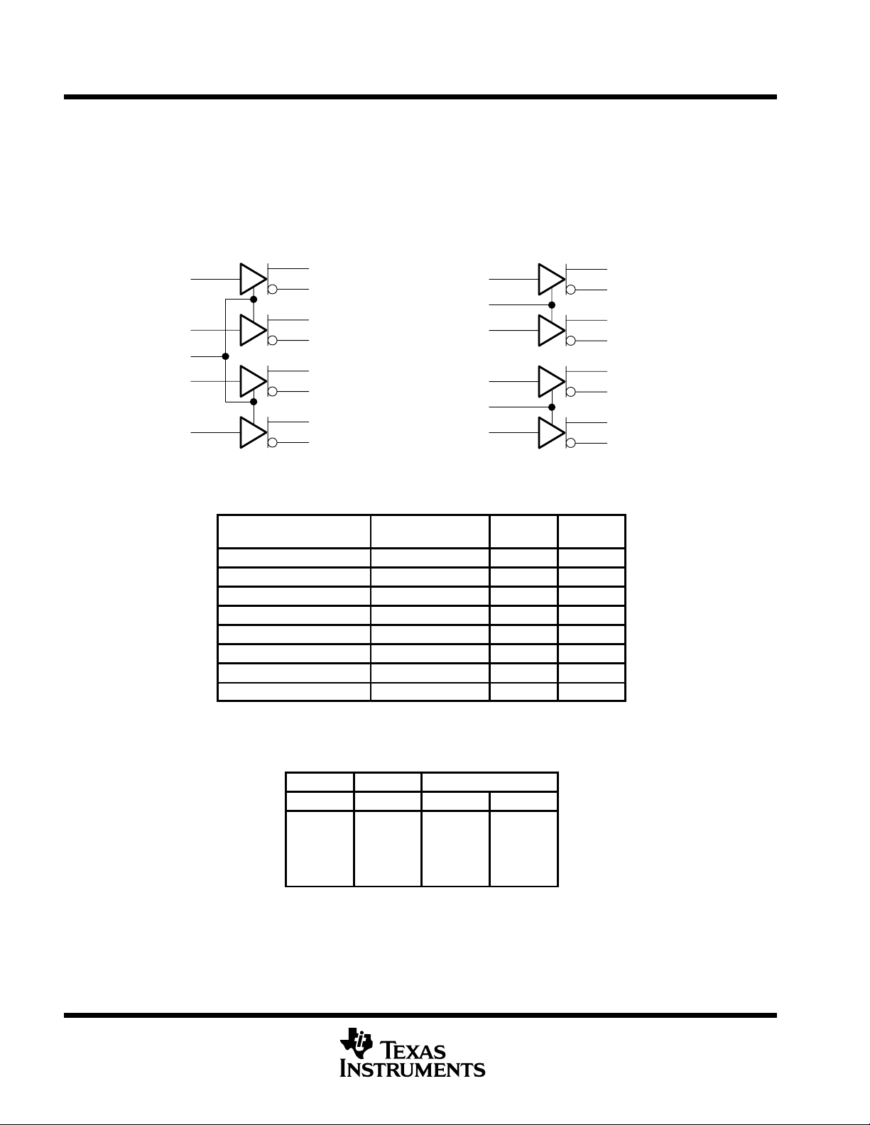
logic diagram (positive logic)
1A
2A
EN
3A
4A
(1/4 of ’LVDS387 or 1/2 of ’LVDS389 shown)
PART NUMBER
SN65LVDS387DGG –40°C to 85°C 16 15 kV
SN75LVDS387DGG 0°C to 70°C 16 4 kV
SN65LVDS389DBT –40°C to 85°C 8 15 kV
SN75LVDS389DBT 0°C to 70°C 8 4 kV
SN65LVDS391D –40°C to 85°C 4 15 kV
SN75LVDS391D 0°C to 70°C 4 4 kV
SN65LVDS391PW –40°C to 85°C 4 15 kV
SN75LVDS391PW 0°C to 70°C 4 4 kV
†
This package is available taped and reeled. To order this packaging option, add
an R suffix to the part number (e.g., SN65LVDS387DGGR).
1Y
1Z
2Y
2Z
3Y
3Z
4Y
4Z
†
EN
EN
AVAILABLE OPTIONS
TEMPERATURE
RANGE
1A
2A
3A
4A
(’LVDS391 shown)
NO. OF
DRIVERS
BUS-PIN
1Y
1Z
2Y
2Z
3Y
3Z
4Y
4Z
ESD
DRIVER FUNCTION TABLE
INPUT
A EN Y Z
H H H L
L H L H
X L Z Z
OPEN H L H
H = high-level, L = low-level, X = irrelevant,
Z = high-impedance (off)
2
POST OFFICE BOX 655303 • DALLAS, TEXAS 75265
ENABLE OUTPUTS

O erating free-air tem erature, T
A
equivalent input and output schematic diagrams
EQUIVALENT OF EACH A OR EN INPUT TYPICAL OF ALL OUTPUTS
V
CC
SN65LVDS387, SN75LVDS387, SN65LVDS389
SN75LVDS389, SN65LVDS391, SN75LVDS391
HIGH-SPEED DIFFERENTIAL LINE DRIVERS
SLLS362D – SEPTEMBER 1999 – REVISED MAY 2001
V
CC
7 V
50 Ω
10 kΩ
300 kΩ
–0.5 V to 4 V. . . . . . . . . . . . . . . . . . . . . . . . . . . . . . . . . . . . . . . . . . . . . . . . . . . . . . . . . .
CC
5 Ω
Y or Z
Output
7 V
†
A or EN
Input
absolute maximum ratings over operating free-air temperature (unless otherwise noted)
Supply voltage range, V
Input voltage range: Inputs –0.5 V to 6 V. . . . . . . . . . . . . . . . . . . . . . . . . . . . . . . . . . . . . . . . . . . . . . . . . . . . . . . . .
Y or Z –0.5 V to 4 V. . . . . . . . . . . . . . . . . . . . . . . . . . . . . . . . . . . . . . . . . . . . . . . . . . . . . . . . .
Electrostatic discharge: SN65’ (Y, Z, and GND) Class 3, A:15 kV, B: 500 V. . . . . . . . . . . . . . . . . . . . . . . . . . . . .
SN75’ (Y, Z, and GND) Class 3, A:4 kV, B: 400 V. . . . . . . . . . . . . . . . . . . . . . . . . . . . . .
Continuous power dissipation (see Dissipation Rating Table). . . . . . . . . . . . . . . . . . . . . . . . . . . . . . . . . . . . . . . .
Storage temperature range –65°C to 150°C. . . . . . . . . . . . . . . . . . . . . . . . . . . . . . . . . . . . . . . . . . . . . . . . . . . . . . . .
Lead temperature 1,6 mm (1/16 in) from case for 10 seconds 260°C. . . . . . . . . . . . . . . . . . . . . . . . . . . . . . . . . .
†
Stresses beyond those listed under “absolute maximum ratings” may cause permanent damage to the device. These are stress ratings only, and
functional operation of the device at these or any other conditions beyond those indicated under “recommended operating conditions” is not
implied. Exposure to absolute-maximum-rated conditions for extended periods may affect device reliability.
NOTES: 1. All voltage values, except differential I/O bus voltages, are with respect to network ground terminal.
‡
This is the inverse of the junction-to-ambient thermal resistance when board-mounted (low-k) and with no air flow.
2. Tested in accordance with MIL-STD-883C Method 3015.7.
DISSIPATION RATING TABLE
PACKAGE
D 950 mW 7.6 mW/°C 608 mW 494 mW
DBT 1071 mW 8.5 mW/°C 688 mW 556 mW
DGG 2094 mW 16.7 mW/°C 1342 mW 1089 mW
PW 774 mW 6.2 mW/°C 496 mW 402 mW
TA ≤ 25°C
DERATING FACTOR
ABOVE TA = 25°C
‡
TA = 70°C
POWER RATING
TA = 85°C
POWER RATING
recommended operating conditions
Supply voltage, V
High-level input voltage, V
Low-level input voltage, V
p
MIN NOM MAX UNIT
CC
IH
IL
p
POST OFFICE BOX 655303 • DALLAS, TEXAS 75265
SN75’ 0 70 °C
SN65’ –40 85 °C
3 3.3 3.6 V
2 V
0.8 V
3
SN65LVDS387, SN75LVDS387, SN65LVDS389
R
100 Ω
Enabled
ICCSupply current
mA
V
IN
V
CC
IOSShort-circuit output current
R
L
100 Ω
L
See Figure 5
SN75LVDS389, SN65LVDS391, SN75LVDS391
HIGH-SPEED DIFFERENTIAL LINE DRIVERS
SLLS362D – SEPTEMBER 1999 – REVISED MAY 2001
electrical characteristics over recommended operating conditions (unless otherwise noted)
PARAMETER TEST CONDITIONS MIN TYP†MAX UNIT
|VOD| Differential output voltage magnitude
∆|VOD|
V
OC(SS)
∆V
OC(SS)
V
OC(PP)
I
IH
I
IL
I
OZ
I
O(OFF)
C
IN
C
O
†
All typical values are at 25°C and with a 3.3-V supply.
Change in differential output voltage
magnitude between logic states
Steady-state common-mode output voltage 1.125 1.375 V
Change in steady-state common-mode output
voltage between logic states
Peak-to-peak common-mode output voltage 50 150 mV
pp
High-level input current VIH = 2 V 3 20 µA
Low-level input current VIL = 0.8 V 2 10 µA
p
High-impedance output current VO = 0 V or V
Power-off output current VCC = 1.5 V, VO = 2.4 V ±1 µA
Input capacitance VI = 0.4 sin (4E6πt) + 0.5 V 5 pF
Output capacitance
=
L
See Figure 1 and Figure 2
See Figure 3
’LVDS387
’LVDS389
’LVDS391
’LVDS387
’LVDS389
’LVDS391
VOY or VOZ = 0 V ±24 mA
VOD = 0 V ±12 mA
VI = 0.4 sin (4E6πt) + 0.5 V,
Disabled
,,
,
RL = 100 Ω,
VIN = 0.8 V or 2 V
Disabled,
= 0 V or
CC
247 340 454
–50 50
–50 50 mV
85 95
50 70
20 26
0.5 1.5
0.5 1.5
0.5 1.3
±1 µA
9.4 pF
mV
switching characteristics over recommended operating conditions (unless otherwise noted)
PARAMETER TEST CONDITIONS MIN TYP†MAX UNIT
t
PLH
t
PHL
t
r
t
f
t
sk(p)
t
sk(o)
t
sk(pp)
t
PZH
t
PZL
t
PHZ
t
PLZ
†
All typical values are at 25°C and with a 3.3-V supply.
‡
t
sk(o)
§
t
sk(pp)
sheet when both devices operate with the same supply voltage, at the same temperature, and have the same test circuits.
Propagation delay time, low-to-high-level output 0.9 1.7 2.9 ns
Propagation delay time, high-to-low-level output 0.9 1.6 2.9 ns
Differential output signal rise time
Differential output signal fall time
Pulse skew (|t
Output skew
Part-to-part skew
Propagation delay time, high-impedance-to-high-level output 6.4 15 ns
Propagation delay time, high-impedance-to-low-level output
Propagation delay time, high-level-to-high-impedance output
Propagation delay time, low-level-to-high-impedance output 4.5 15 ns
is the magnitude of the time difference between the t
is the magnitude of the difference in propagation delay times between any specified terminals of any two devices characterized in this data
‡
PHL
– t
|)
PLH
§
or t
PLH
of all drivers of a single device with all of their inputs connected together.
PHL
=
CL = 10 pF,
See Figure 4
,
0.4 0.8 1 ns
0.4 0.8 1 ns
150 500 ps
80 150 ps
1.5 ns
5.9 15 ns
3.5 15 ns
4
POST OFFICE BOX 655303 • DALLAS, TEXAS 75265
SN65LVDS387, SN75LVDS387, SN65LVDS389
SN75LVDS389, SN65LVDS391, SN75LVDS391
HIGH-SPEED DIFFERENTIAL LINE DRIVERS
SLLS362D – SEPTEMBER 1999 – REVISED MAY 2001
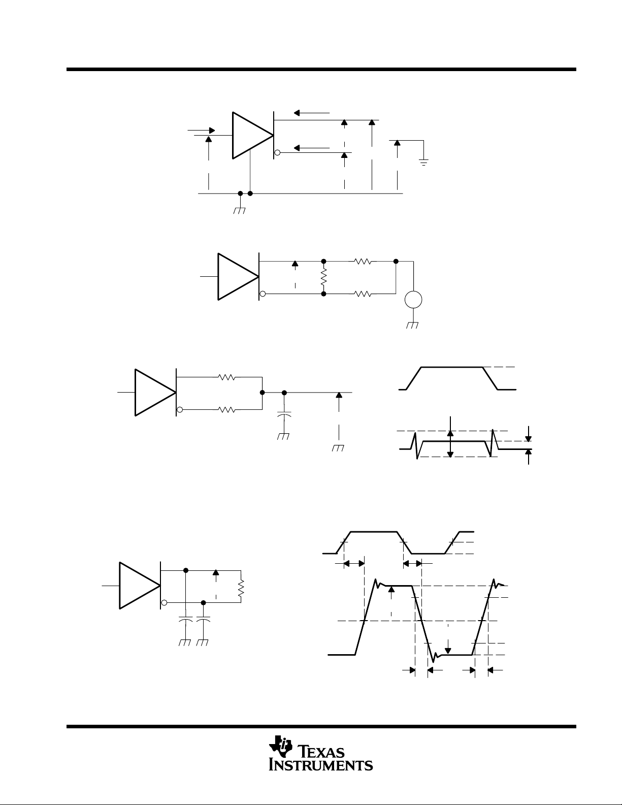
PARAMETER MEASUREMENT INFORMATION
I
OY
GND
Y
V
I
OZ
Z
OD
V
OY
V
V
OZ
OC
(VOY + VOZ)/2
I
I
A
V
I
Figure 1. Voltage and Current Definitions
Input
Y
V
OD
Z
100 Ω
3.75 kΩ
3.75 kΩ
±
0 V ≤ V
TEST
≤ 2.4 V
Figure 2. VOD Test Circuit
49.9 Ω ± 1% (2 Places)
Y
V
Input
Z
50 pF
NOTE: All input pulses are supplied by a generator having the following characteristics: tr or tf ≤ 1 ns, pulse repetition rate (PRR) = 0.5 Mpps,
pulse width = 500 ± 10 ns. CL includes instrumentation and fixture capacitance within 0,06 m of the D.U.T . The measurement of V
is made on test equipment with a –3 dB bandwidth of at least 300 MHz.
V
OC
I
V
OC(PP)
V
O
3 V
0 V
V
OC(SS)
OC(PP)
Figure 3. Test Circuit and Definitions for the Driver Common-Mode Output V oltage
Input
t
Y
PLH
t
PHL
2 V
1.4 V
0.8 V
Input
Z
NOTE: All input pulses are supplied by a generator having the following characteristics: tr or tf ≤ 1 ns, pulse repetition rate (PRR) = 50 Mpps, pulse
width = 10 ± 0.2 ns. CL includes instrumentation and fixture capacitance within 0,06 m of the D.U.T.
V
OD
CL = 10 pF
(2 Places)
100 Ω ± 1 %
Output
0 V
V
OD(H)
V
OD(L)
t
f
t
r
100%
80%
20%
0%
Figure 4. Test Circuit, Timing, and Voltage Definitions for the Differential Output Signal
POST OFFICE BOX 655303 • DALLAS, TEXAS 75265
5

SN65LVDS387, SN75LVDS387, SN65LVDS389
SN75LVDS389, SN65LVDS391, SN75LVDS391
HIGH-SPEED DIFFERENTIAL LINE DRIVERS
SLLS362D – SEPTEMBER 1999 – REVISED MAY 2001
PARAMETER MEASUREMENT INFORMATION
Y
0.8 V or 2 V
Input
Input
t
PZH
V
OY
or
V
OZ
t
PZL
V
OZ
or
V
OY
NOTE: All input pulses are supplied by a generator having the following characteristics: tr or tf ≤ 1 ns, pulse repetition rate (PRR) = 0.5 Mpps,
pulse width = 500 ± 10 ns. CL includes instrumentation and fixture capacitance within 0,06 m of the D.U.T.
Z
CL = 10 pF
(2 Places)
49.9 Ω ± 1% (2 Places)
V
OYVOZ
2 V
1.4 V
0.8 V
t
PHZ
≅ 1.4 V
1.3 V
1.2 V
t
PLZ
1.2 V
1.1 V
≅ 1 V
+
1.2 V
–
Figure 5. Enable and Disable Time Circuit and Definitions
6
POST OFFICE BOX 655303 • DALLAS, TEXAS 75265

SN65LVDS387, SN75LVDS387, SN65LVDS389
SN75LVDS389, SN65LVDS391, SN75LVDS391
HIGH-SPEED DIFFERENTIAL LINE DRIVERS
SLLS362D – SEPTEMBER 1999 – REVISED MAY 2001
TYPICAL CHARACTERISTICS
’LVDS391
SUPPLY CURRENT (RMS)
vs
SWITCHING FREQUENCY
60
All outputs loaded and enabled.
50
240
220
40
30
– Supply Current – mA
20
CC
I
10
0
0 50 100 150 200 250 300
’LVDS387
SUPPLY CURRENT (RMS)
vs
SWITCHING FREQUENCY
VCC = 3.6 V
VCC = 3.3 V
VCC = 3 V
f – Frequency – MHz
Figure 6
’LVDS389
SUPPLY CURRENT (RMS)
vs
SWITCHING FREQUENCY
110
100
200
180
160
140
– Supply Current – mA
CC
120
I
100
80
0 50 100 150 200 250 300 350
VCC = 3.6 V
VCC = 3.3 V
VCC = 3 V
All outputs loaded and enabled.
f – Frequency – MHz
Figure 7
90
80
70
– Supply Current – mA
60
CC
I
50
40
0 50 100 150 200 250 300
POST OFFICE BOX 655303 • DALLAS, TEXAS 75265
VCC = 3.6 V
VCC = 3.3 V
VCC = 3 V
All outputs loaded and enabled.
f – Frequency – MHz
Figure 8
7

SN65LVDS387, SN75LVDS387, SN65LVDS389
SN75LVDS389, SN65LVDS391, SN75LVDS391
HIGH-SPEED DIFFERENTIAL LINE DRIVERS
SLLS362D – SEPTEMBER 1999 – REVISED MAY 2001
TYPICAL CHARACTERISTICS
LOW-TO-HIGH PROPAGATION DELAY TIME
vs
FREE-AIR TEMPERATURE
2.1
2.0
1.9
1.8
1.7
1.6
1.5
1.4
PLH – Low-To-High Propagation Delay Time – ns
t
1.3
–40 –20 0 20 40 60 80 100
VCC = 3.6 V
VCC = 3 V
VCC = 3.3 V
TA – Free-Air Temperature – °C
Figure 9
LOW-LEVEL OUTPUT VOLTAGE
vs
4
LOW-LEVEL OUTPUT CURRENT
VCC = 3.3 V
TA = 25°C
HIGH-TO-LOW PROPAGATION DELAY TIME
vs
FREE-AIR TEMPERATURE
2.2
2.0
VCC = 3 V
1.8
1.6
1.4
1.2
PHL – High-To-Low Propagation Delay Time – ns
t
1.0
–40 –20 0 20 40 60 80 100
Ta – Free-Air Temperature – °C
VCC = 3.3 V
VCC = 3.6 V
Figure 10
HIGH-LEVEL OUTPUT VOLTAGE
vs
3.5
3
HIGH-LEVEL OUTPUT CURRENT
VCC = 3.3 V
TA = 25°C
3
2
– Low-Level Output Voltage – V
1
OL
V
0
0
IOL – Low-Level Output Current – mA
2
46
Figure 11
8
POST OFFICE BOX 655303 • DALLAS, TEXAS 75265
– High-Level Output Voltage – V
V
OH
2.5
1.5
0.5
2
1
0
–4
–3
IOH – High-Level Output Current – mA
–20
–1
Figure 12

SN65LVDS387, SN75LVDS387, SN65LVDS389
SN75LVDS389, SN65LVDS391, SN75LVDS391
HIGH-SPEED DIFFERENTIAL LINE DRIVERS
SLLS362D – SEPTEMBER 1999 – REVISED MAY 2001
TYPICAL CHARACTERISTICS
OUTPUT VOLTAGE
vs
TIME
V
OY
V
OZ
V
OD
– Output Voltage – V
O
V
t – Time – ns
Figure 13
POST OFFICE BOX 655303 • DALLAS, TEXAS 75265
9

SN65LVDS387, SN75LVDS387, SN65LVDS389
SN75LVDS389, SN65LVDS391, SN75LVDS391
HIGH-SPEED DIFFERENTIAL LINE DRIVERS
SLLS362D – SEPTEMBER 1999 – REVISED MAY 2001
APPLICATION INFORMATION
Host
Controller
SN65LVDS387 or 389
Host
DBn
DBn–1
DBn–2
DBn–3
DB2
DB1
DB0
TX Clock
Power Power
Balanced Interconnect
T
T
T
T
T
T
T
T
Indicates twisting of the
conductors.
Target
DBn
DBn–1
DBn–2
DBn–3
DB2
DB1
DB0
RX Clock
LVDS Receiver(s)
Indicates the line termination
T
circuit.
Target
Controller
Figure 14. Typical Application Schematic
Signaling Rate vs Distance
The ultimate data transfer rate over a given cable or trace length involves many variables. Starting with the
capabilities of this LVDS driver to reproduce a data pulse as short as 1.6 ns (a 630 Mbps signaling rate) with
less than 500 ps of pulse distortion, any degradation of this pulse by the transmission media will necessarily
reduce the timing margin at the receiving end of the data link.
The timing uncertainty induced by the transmission media is commonly referred to as jitter and comes from
numerous sources. The characteristics of a particular transmission media can be quantified by using an
eyepattern measurement such as shown in Figure 12, which shows about 340 ps of jitter or 20% of the data
pulse width.
10
POST OFFICE BOX 655303 • DALLAS, TEXAS 75265

LENGTH
SN65LVDS387, SN75LVDS387, SN65LVDS389
SN75LVDS389, SN65LVDS391, SN75LVDS391
HIGH-SPEED DIFFERENTIAL LINE DRIVERS
SLLS362D – SEPTEMBER 1999 – REVISED MAY 2001
APPLICATION INFORMATION
height
abs.
jitter
width
unit interval
Figure 15. Typical LVDS Eyepattern
A generally accepted range of jitter at the receiver inputs that allows data recovery is 5% to 20% of the unit
interval (data pulse width). Table 1 shows the signaling rate achieved on various cables and lengths at a 5%
eyepattern jitter with a typical LVDS driver.
Table 1. Signaling Rates for Various Cables for 5% Eyepattern Jitter
†
CABLE
(m)
1 240 200 240 270 180 230
5 205 210 230 250 215 230
10 180 150 195 200 145 180
†
Cable A: CAT 3, specified up to 16 MHz, no shield, outside conductor diameter (∅) 0.52 mm
Cable B: CAT 5, specified up to 100 MHz, no shield, ∅ 0.52 mm
Cable C: CAT 5, specified up to 100 MHz, taped over all shield, ∅ 0.52 mm
Cable D: CAT 5 (exceeding CAT 5), specified up to 300 MHz, braided over all shield plus taped individual shield for any
Cable E: CAT 5 (exceeding CAT 5), specified up to 350 MHz, ∅ 0.64 mm (AWG22), no shield
Cable F: CAT 5 (exceeding CAT 5), specified up to 350 MHz, “self-shielded”, ∅0.64 mm (AWG22)
A
(Mbps)
pair, ∅ 0.64 mm (A WG22)
B
(Mbps)
C
(Mbps)
D
(Mbps)
E
(Mbps)
F
(Mbps)
During synchronous parallel transfers, skew between the data and clock lines will also reduce the timing margin.
This must be accounted for in the system timing budget. Fortunately, the low output skew of this L VDS driver
will generally be a small portion of this budget.
other LVDS products
For other products and applications notes in the LVDS and LVDM product families visit our Web site at
http://www.ti.com/sc/datatran.
POST OFFICE BOX 655303 • DALLAS, TEXAS 75265
11

SN65LVDS387, SN75LVDS387, SN65LVDS389
SN75LVDS389, SN65LVDS391, SN75LVDS391
HIGH-SPEED DIFFERENTIAL LINE DRIVERS
SLLS362D – SEPTEMBER 1999 – REVISED MAY 2001
MECHANICAL DATA
D (R-PDSO-G**) PLASTIC SMALL-OUTLINE PACKAGE
14 PINS SHOWN
0.050 (1,27)
14
1
0.069 (1,75) MAX
A
0.020 (0,51)
0.014 (0,35)
0.010 (0,25)
0.004 (0,10)
DIM
8
7
PINS **
0.010 (0,25)
0.157 (4,00)
0.150 (3,81)
M
0.244 (6,20)
0.228 (5,80)
Seating Plane
0.004 (0,10)
8
14
0.008 (0,20) NOM
0°–8°
16
Gage Plane
0.010 (0,25)
0.044 (1,12)
0.016 (0,40)
A MAX
A MIN
NOTES: A. All linear dimensions are in inches (millimeters).
12
B. This drawing is subject to change without notice.
C. Body dimensions do not include mold flash or protrusion, not to exceed 0.006 (0,15).
D. Falls within JEDEC MS-012
POST OFFICE BOX 655303 • DALLAS, TEXAS 75265
0.197
(5,00)
0.189
(4,80)
0.344
(8,75)
0.337
(8,55)
0.394
(10,00)
0.386
(9,80)
4040047/D 10/96

SN65LVDS387, SN75LVDS387, SN65LVDS389
SN75LVDS389, SN65LVDS391, SN75LVDS391
HIGH-SPEED DIFFERENTIAL LINE DRIVERS
SLLS362D – SEPTEMBER 1999 – REVISED MAY 2001
MECHANICAL DATA
DBT (R-PDSO-G**) PLASTIC SMALL-OUTLINE PACKAGE
30 PINS SHOWN
0,50
30
1
1,20 MAX
0,27
0,17
16
4,50
4,30
15
A
Seating Plane
0,15
0,05
0,08
M
0,15 NOM
6,60
6,20
Gage Plane
0,25
0°–8°
0,75
0,50
0,10
PINS **
DIM
A MAX
A MIN
NOTES: A. All linear dimensions are in millimeters.
B. This drawing is subject to change without notice.
C. Body dimensions do not include mold flash or protrusion.
D. Falls within JEDEC MO-153
28
7,90
7,70
30
7,90
7,70
38
9,80 11,10
44
50
12,60
12,409,60 10,90
4073252/D 09/97
POST OFFICE BOX 655303 • DALLAS, TEXAS 75265
13

SN65LVDS387, SN75LVDS387, SN65LVDS389
SN75LVDS389, SN65LVDS391, SN75LVDS391
HIGH-SPEED DIFFERENTIAL LINE DRIVERS
SLLS362D – SEPTEMBER 1999 – REVISED MAY 2001
MECHANICAL DATA
DGG (R-PDSO-G**) PLASTIC SMALL-OUTLINE PACKAGE
48 PINS SHOWN
0,50
48
1
1,20 MAX
0,27
0,17
25
24
A
0,15
0,05
0,08
M
8,30
6,20
7,90
6,00
Seating Plane
0,10
0,15 NOM
Gage Plane
0,25
0°–8°
0,75
0,50
DIM
NOTES: A. All linear dimensions are in millimeters.
B. This drawing is subject to change without notice.
C. Body dimensions do not include mold protrusion not to exceed 0,15.
D. Falls within JEDEC MO-153
PINS **
A MAX
A MIN
48
12,60
12,40
56
14,10
13,90
64
17,10
16,90
4040078/F 12/97
14
POST OFFICE BOX 655303 • DALLAS, TEXAS 75265

SN65LVDS387, SN75LVDS387, SN65LVDS389
SN75LVDS389, SN65LVDS391, SN75LVDS391
HIGH-SPEED DIFFERENTIAL LINE DRIVERS
SLLS362D – SEPTEMBER 1999 – REVISED MAY 2001
MECHANICAL DATA
PW (R-PDSO-G**) PLASTIC SMALL-OUTLINE PACKAGE
14 PINS SHOWN
0,65
1,20 MAX
14
0,30
0,19
8
4,50
4,30
PINS **
7
Seating Plane
0,15
0,05
8
1
A
DIM
6,60
6,20
14
0,10
0,10
M
0,15 NOM
Gage Plane
0,25
0°–8°
2016
24
28
0,75
0,50
A MAX
A MIN
NOTES: A. All linear dimensions are in millimeters.
B. This drawing is subject to change without notice.
C. Body dimensions do not include mold flash or protrusion not to exceed 0,15.
D. Falls within JEDEC MO-153
3,10
2,90
5,10
4,90
5,10
4,90
6,60
6,40
7,90
7,70
9,80
9,60
4040064/F 01/97
POST OFFICE BOX 655303 • DALLAS, TEXAS 75265
15

PACKAGE OPTION ADDENDUM
www.ti.com
14-Mar-2005
PACKAGING INFORMATION
Orderable Device Status
(1)
Package
Type
Package
Drawing
Pins Package
Qty
Eco Plan
SN65LVDS387DGG ACTIVE TSSOP DGG 64 25 None CU NIPDAU Level-1-220C-UNLIM
SN65LVDS387DGGR ACTIVE TSSOP DGG 64 2000 None CU NIPDAU Level-1-220C-UNLIM
SN65LVDS389DBT ACTIVE SM8 DBT 38 50 None CU NIPDAU Level-2-220C-1 YEAR
SN65LVDS389DBTG4 PREVIEW SM8 DBT 38 50 None Call TI Call TI
SN65LVDS389DBTR ACTIVE SM8 DBT 38 2000 None CU NIPDAU Level-2-220C-1 YEAR
SN65LVDS389DBTRG4 PREVIEW SM8 DBT 38 2000 None Call TI Call TI
SN65LVDS391D ACTIVE SOIC D 16 40 Pb-Free
SN65LVDS391DR ACTIVE SOIC D 16 2500 Pb-Free
SN65LVDS391PW ACTIVE TSSOP PW 16 90 None CU NIPDAU Level-1-220C-UNLIM
SN65LVDS391PWR ACTIVE TSSOP PW 16 2000 None CU NIPDAU Level-1-220C-UNLIM
SN75LVDS387DGG ACTIVE TSSOP DGG 64 25 None CU NIPDAU Level-1-220C-UNLIM
SN75LVDS387DGGR ACTIVE TSSOP DGG 64 2000 None CU NIPDAU Level-1-220C-UNLIM
SN75LVDS389DBT ACTIVE SM8 DBT 38 50 None CU NIPDAU Level-2-220C-1 YEAR
SN75LVDS389DBTG4 ACTIVE SM8 DBT 38 50 Green (RoHS &
no Sb/Br)
SN75LVDS389DBTR ACTIVE SM8 DBT 38 2000 None CU NIPDAU Level-2-220C-1 YEAR
SN75LVDS389DBTRG4 ACTIVE SM8 DBT 38 2000 Green(RoHS &
no Sb/Br)
SN75LVDS391D ACTIVE SOIC D 16 40 Pb-Free
SN75LVDS391DR ACTIVE SOIC D 16 2500 Pb-Free
SN75LVDS391PW ACTIVE TSSOP PW 16 90 None CU NIPDAU Level-1-220C-UNLIM
SN75LVDS391PWR ACTIVE TSSOP PW 16 2000 None CU NIPDAU Level-1-220C-UNLIM
(1)
The marketing status values are defined as follows:
ACTIVE: Product device recommended for new designs.
LIFEBUY: TI has announced that the device will be discontinued, and a lifetime-buy period is in effect.
NRND: Not recommended for new designs. Device is in production to support existing customers, but TI does not recommend using this part in
a new design.
PREVIEW: Device has been announced but is not in production. Samples may or may not be available.
OBSOLETE: TI has discontinued the production of the device.
(RoHS)
(RoHS)
(RoHS)
(RoHS)
(2)
Lead/Ball Finish MSL Peak Temp
CU NIPDAU Level-2-260C-1YEAR/
Level-1-220C-UNLIM
CU NIPDAU Level-2-260C-1YEAR/
Level-1-220C-UNLIM
CU NIPDAU Level-2-260C-1 YEAR
CU NIPDAU Level-2-260C-1 YEAR
CU NIPDAU Level-2-260C-1YEAR/
Level-1-220C-UNLIM
CU NIPDAU Level-2-260C-1YEAR/
Level-1-220C-UNLIM
(3)
(2)
Eco Plan - May not be currently available - please check http://www.ti.com/productcontent for the latest availability information and additional
product content details.
None: Not yet available Lead (Pb-Free).
Pb-Free (RoHS): TI's terms "Lead-Free" or "Pb-Free" mean semiconductor products that are compatible with the current RoHS requirements
for all 6 substances, including the requirement that lead not exceed 0.1% by weight in homogeneous materials. Where designed to be soldered
at high temperatures, TI Pb-Free products are suitable for use in specified lead-free processes.
Green (RoHS & no Sb/Br): TI defines "Green" to mean "Pb-Free" and in addition, uses package materials that do not contain halogens,
including bromine (Br) or antimony (Sb) above 0.1% of total product weight.
(3)
MSL, Peak Temp. -- The Moisture Sensitivity Level rating according to the JEDECindustry standard classifications, and peak solder
temperature.
Important Information and Disclaimer:The information provided on this page represents TI's knowledge and belief as of the date that it is
provided. TI bases its knowledge and belief on information provided by third parties, and makes no representation or warranty as to the
accuracy of such information. Efforts are underway to better integrate information from third parties. TI has taken and continues to take
Addendum-Page 1

PACKAGE OPTION ADDENDUM
www.ti.com
reasonable steps to provide representative and accurate information but may not have conducted destructive testing or chemical analysis on
incoming materials and chemicals. TI and TI suppliers consider certain information to be proprietary, and thus CAS numbers and other limited
information may not be available for release.
In no event shall TI's liability arising out of such information exceed the total purchase price of the TI part(s) at issue in this document sold by TI
to Customer on an annual basis.
14-Mar-2005
Addendum-Page 2

IMPORTANT NOTICE
Texas Instruments Incorporated and its subsidiaries (TI) reserve the right to make corrections, modifications,
enhancements, improvements, and other changes to its products and services at any time and to discontinue
any product or service without notice. Customers should obtain the latest relevant information before placing
orders and should verify that such information is current and complete. All products are sold subject to TI’s terms
and conditions of sale supplied at the time of order acknowledgment.
TI warrants performance of its hardware products to the specifications applicable at the time of sale in
accordance with TI’s standard warranty. Testing and other quality control techniques are used to the extent TI
deems necessary to support this warranty . Except where mandated by government requirements, testing of all
parameters of each product is not necessarily performed.
TI assumes no liability for applications assistance or customer product design. Customers are responsible for
their products and applications using TI components. To minimize the risks associated with customer products
and applications, customers should provide adequate design and operating safeguards.
TI does not warrant or represent that any license, either express or implied, is granted under any TI patent right,
copyright, mask work right, or other TI intellectual property right relating to any combination, machine, or process
in which TI products or services are used. Information published by TI regarding third-party products or services
does not constitute a license from TI to use such products or services or a warranty or endorsement thereof.
Use of such information may require a license from a third party under the patents or other intellectual property
of the third party, or a license from TI under the patents or other intellectual property of TI.
Reproduction of information in TI data books or data sheets is permissible only if reproduction is without
alteration and is accompanied by all associated warranties, conditions, limitations, and notices. Reproduction
of this information with alteration is an unfair and deceptive business practice. TI is not responsible or liable for
such altered documentation.
Resale of TI products or services with statements different from or beyond the parameters stated by TI for that
product or service voids all express and any implied warranties for the associated TI product or service and
is an unfair and deceptive business practice. TI is not responsible or liable for any such statements.
Following are URLs where you can obtain information on other Texas Instruments products and application
solutions:
Products Applications
Amplifiers amplifier.ti.com Audio www.ti.com/audio
Data Converters dataconverter.ti.com Automotive www.ti.com/automotive
DSP dsp.ti.com Broadband www.ti.com/broadband
Interface interface.ti.com Digital Control www.ti.com/digitalcontrol
Logic logic.ti.com Military www.ti.com/military
Power Mgmt power.ti.com Optical Networking www.ti.com/opticalnetwork
Microcontrollers microcontroller.ti.com Security www.ti.com/security
Telephony www.ti.com/telephony
Video & Imaging www.ti.com/video
Wireless www.ti.com/wireless
Mailing Address: Texas Instruments
Post Office Box 655303 Dallas, Texas 75265
Copyright 2005, Texas Instruments Incorporated

Copyright © Each Manufacturing Company.
All Datasheets cannot be modified without permission.
This datasheet has been download from :
www.AllDataSheet.com
100% Free DataSheet Search Site.
Free Download.
No Register.
Fast Search System.
www.AllDataSheet.com
 Loading...