

Datasheet SN75LVDM976DGG, SN75LVDM976DGGR, SN75LVDM976DL, SN75LVDM976DLR, SN75LVDM977DGG Datasheet (Texas Instruments)
...
SN75LVDM976, SN75LVDM977
9-CHANNEL DUAL-MODE TRANSCEIVERS
SLLS292B – APRIL 1998 – REVISED JANUARY 2000
1
POST OFFICE BOX 655303 • DALLAS, TEXAS 75265
D
9 Channels for the Data and Control Paths
of the Small Computer Systems Interface
(SCSI)
D
Supports Single-Ended and Low-Voltage
Differential (LVD) SCSI
D
CMOS Input Levels (’LVDM976) or TTL
Input Levels (’LVDM977) Available
D
Includes DIFFSENS Comparators on CDE0
D
Single-Ended Receivers Include Noise
Pulse Rejection Circuitry
D
Packaged in Thin Shrink Small-Outline
Package With 20-Mil Terminal Pitch
D
Low Disabled Supply Current 7 mA
Maximum
D
Power-Up/Down Glitch Protection
D
Bus is High-Impedance With VCC = 1.5 V
D
Pin-Compatible With the SN75976ADGG
High-Voltage Differential Transceiver
description
The SN75LVDM976 and SN75LVDM977 have
nine transceivers for transmitting or receiving the
signals to or from a SCSI data bus. They offer
electrical compatibility to both the single-ended
signaling of X3.277:1996–SCSI–3 Parallel Interface (Fast–20) and the new low-voltage differential signaling method of proposed standard
1142–D SCSI Parallel Interface – 2 (SPI–2).
The differential drivers are nonsymmetrical. The
SCSI bus uses a dc bias on the line to allow
terminated fail safe and wired-OR signaling. This bias can be as high as 125 mV and induces a difference in
the high-to-low and low-to-high transition times of a symmetrical driver. In order to reduce pulse skew, an LVD
SCSI driver’s output characteristics become nonsymmetrical. In other words, there is more assertion current
than negation current to or from the driver. This allows the actual differential signal voltage on the bus to be
symmetrical about 0 V. Even though the driver output characteristics are nonsymmetrical, the design of the
’L VDM976 drivers maintains balanced signaling. Balanced means that the current that flows in each signal line
is nearly equal but opposite in direction and is one of the keys to the low-noise performance of a differential bus.
AVAILABLE OPTIONS
PACKAGE
T
A
TSSOP
(DGG)
CMOS INPUT LEVELS
TSSOP
(DGG)
TTL INPUTS LEVELS
0°C to 70°C
SN75LVDM976DGG
SN75LVDM976DGGR
†
SN75LVDM977DGG
SN75LVDM977DGGR
†
†
The R suffix designates a taped and reeled package.
Copyright 2000, Texas Instruments Incorporated
PRODUCTION DATA information is current as of publication date.
Products conform to specifications per the terms of Texas Instruments
standard warranty. Production processing does not necessarily include
testing of all parameters.
Please be aware that an important notice concerning availability, standard warranty, and use in critical applications of
Texas Instruments semiconductor products and disclaimers thereto appears at the end of this data sheet.
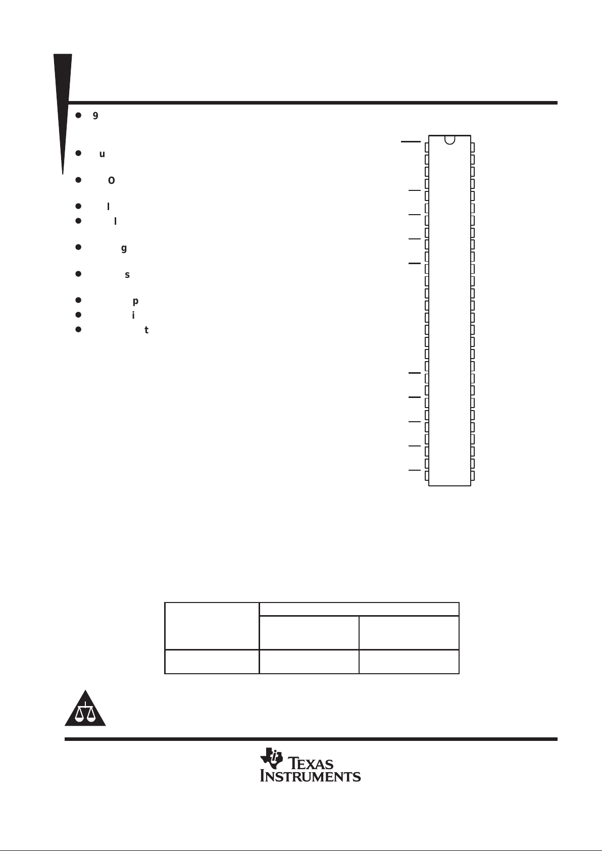
DGG PACKAGE
(TOP VIEW)
1
2
3
4
5
6
7
8
9
10
11
12
13
14
15
16
17
18
19
20
21
22
23
24
25
26
27
28
56
55
54
53
52
51
50
49
48
47
46
45
44
43
42
41
40
39
38
37
36
35
34
33
32
31
30
29
INV/NON
GND
GND
1A
1DE/RE
2A
2DE/RE
3A
3DE/RE
4A
4DE/RE
V
CC
GND
GND
GND
GND
GND
V
CC
5A
5DE/RE
6A
6DE/RE
7A
7DE/RE
8A
8DE/RE
9A
9DE/RE
CDE2
CDE1
CDE0
9B+
9B
–
8B+
8B
–
7B+
7B
–
6B+
6B
–
V
CC
GND
GND
GND
GND
GND
V
CC
5B+
5B
–
4B+
4B
–
3B+
3B
–
2B+
2B
–
1B+
1B
–

SN75LVDM976, SN75LVDM977
9-CHANNEL DUAL-MODE TRANSCEIVERS
SLLS292B – APRIL 1998 – REVISED JANUARY 2000
2
POST OFFICE BOX 655303 • DALLAS, TEXAS 75265
description (continued)
The signal symmetry requirements of the L VD-SCSI bus mean you can no longer obtain logical inversion of a
signal by simply reversing the differential signal connections. This requires the ability to invert the logic
convention through the INV/NON terminal. This input would be a low for SCSI controllers with active-high data
and high for active-low data. In either case, the B+ signals of the transceiver must be connected to the SIGNAL+
line of the SCSI bus and the B– of the transceiver to the SIGNAL– line.
The CDE0 input incorporates a window comparator to detect the status of the DIFFSENS line of a SCSI bus.
This line is below 0.5 V, if using single-ended signals, between 1.7 V and 1.9 V if low-voltage differential, and
between 2.4 V and 5.5 V if high-voltage differential. The outputs assume the characteristics of single-ended or
L VD accordingly or place the outputs into high-impedance, when HVD is detected. This, and the INV/NON
input,
are the only differences to the trade-standard function of the SN75976A HVD transceiver.
Two options are offered to minimize the signal noise margins on the interface between the communications
controller and the transceiver. The SN75LVDM976 has logic input voltage thresholds of about 0.5 VCC. The
SN75L VDM977 has a fixed logic input voltage threshold of about 1.5 V. The input voltage threshold should be
selected to be near the middle of the output voltage swing of the corresponding driver circuit.
The SN75L VDM976 and SN75L VDM977 are characterized for operation over an free-air temperature range of
T
A
= 0°C to 70°C.
SN75LVDM976, SN75LVDM977
9-CHANNEL DUAL-MODE TRANSCEIVERS
SLLS292B – APRIL 1998 – REVISED JANUARY 2000
3
POST OFFICE BOX 655303 • DALLAS, TEXAS 75265
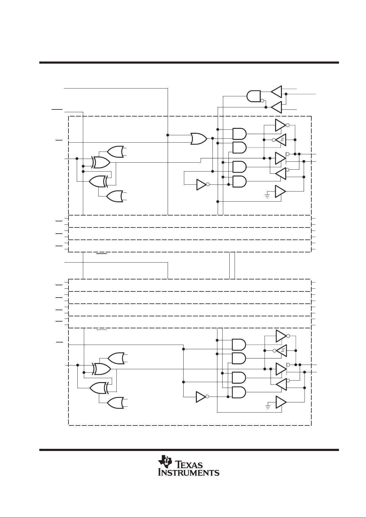
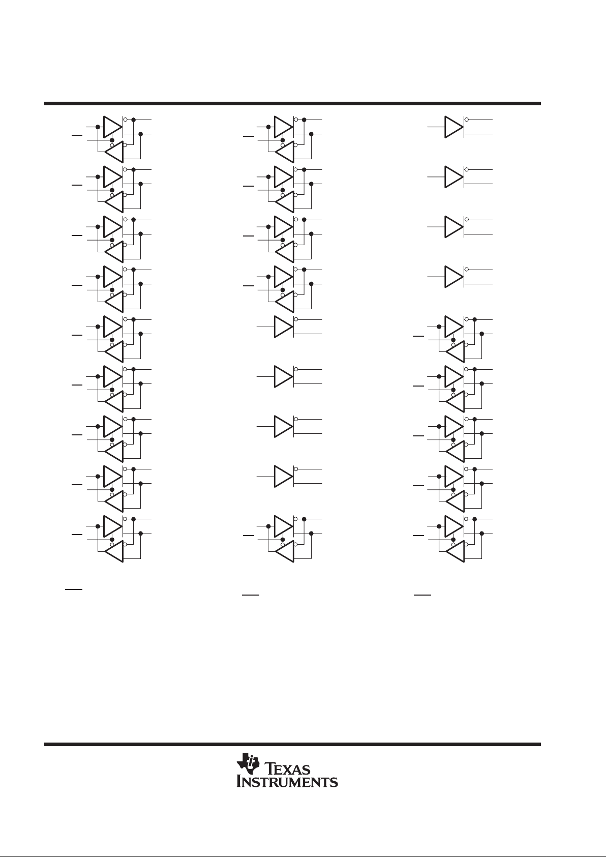
logic diagram (positive logic)
1B–
2B–
2B+
3B–
3B+
4B–
4B+
Channel 4
Channel 3
Channel 2
4DE/RE
4A
3DE/RE
3A
2DE/RE
2A
1DE/RE
1A
CDE1
CDE0
+
–
–
+
1B+
INV/NON
5B–
5B+
6B–
6B+
7B–
7B+
Channel 7
Channel 6
Channel 5
7DE/RE
7A
6DE/RE
6A
5DE/RE
5A
8B–
8B+
Channel 8
8DE/RE
8A
2.4 V
(Internal)
0.5 V
(Internal)
CDE2
9B–
9DE/RE
9A
9B+
1DEb
1DEa
1REb
1REa
SE
LVD
SE LVD
SE LVDINV/NON
INV/NON
9DEb
9DEa
9REb
9REa
1DEb
1REb
1DEa
1REa
9DEb
9REb
9DEa
9REa
A
B
B–
B+
A
DE/RE
V
ID
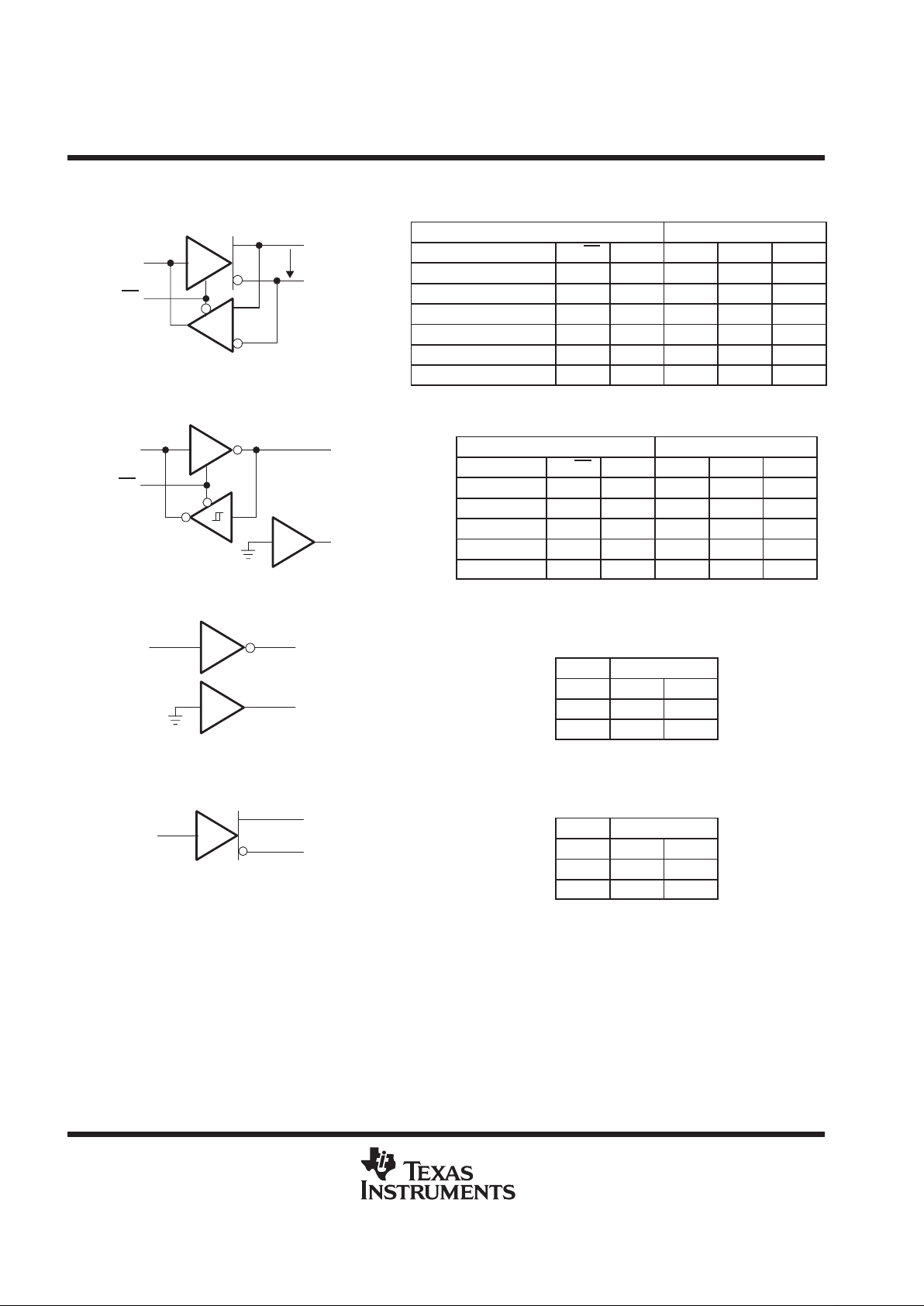
Figure 1. Inverting LVD Transceiver
B–
B+
A
DE/RE
Figure 2. Inverting Single-Ended Transceiver
B–
B+
A
Figure 3. Inverting Single-Ended Driver
B–
B+
A
Figure 4. Inverting LVD Driver
SN75LVDM976, SN75LVDM977
9-CHANNEL DUAL-MODE TRANSCEIVERS
SLLS292B – APRIL 1998 – REVISED JANUARY 2000
4
POST OFFICE BOX 655303 • DALLAS, TEXAS 75265
logic diagrams and function tables
FUNCTION TABLE
Inputs
Outputs
(B+ – B–) DE/RE A B+ B– A
VID ≥ 30 mV L NA Z Z L
–30 mV < VID < 30 mV L NA Z Z ?
VID –30 mV L NA Z Z H
Open circuit L NA Z Z ?
NA H L H L Z
NA H H L H Z
FUNCTION TABLE
Inputs
Outputs
B– DE/RE A B+ B– A
H L NA L Z L
L L NA L Z H
Open circuit L NA L Z ?
NA H L L H Z
NA H H L L Z
FUNCTION TABLE
Input
Outputs
A B+ B–
L L H
H L L
FUNCTION TABLE
Input
Outputs
A B+ B–
L H L
H L H
B–
B+
A
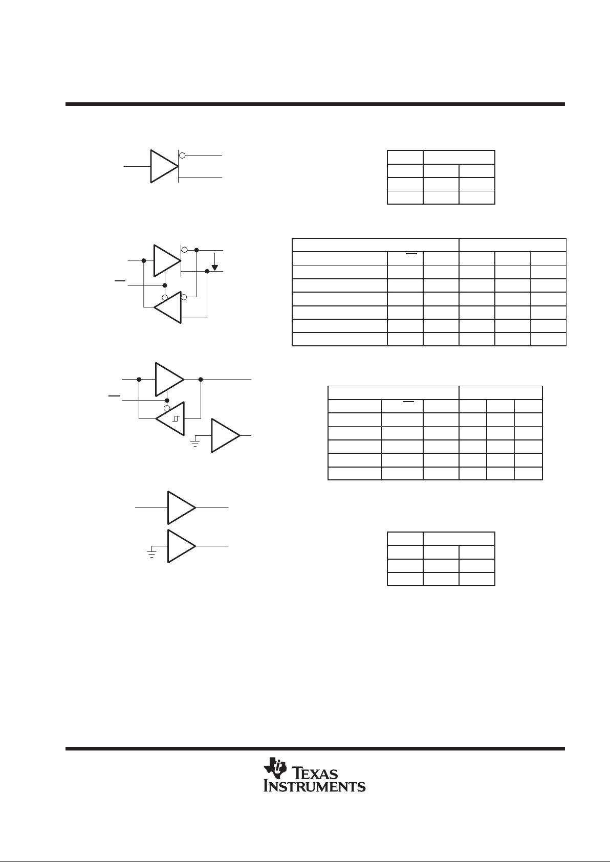
Figure 5. Noninverting LVD Driver
B–
B+
A
DE/RE
V
ID
Figure 6. Noninverting LVD Transceiver
B–
B+
A
DE/RE
Figure 7. Noninverting Single-Ended Transceiver
B–
B+
A
Figure 8. Noninverting Single-Ended Driver
SN75LVDM976, SN75LVDM977
9-CHANNEL DUAL-MODE TRANSCEIVERS
SLLS292B – APRIL 1998 – REVISED JANUARY 2000
5
POST OFFICE BOX 655303 • DALLAS, TEXAS 75265
logic diagrams and function tables (continued)
FUNCTION TABLE
Input
Outputs
A B+ B–
L L H
H H L
FUNCTION TABLE
Inputs
Outputs
(B+ – B–) DE/RE A B+ B– A
VID ≥ 30 mV L NA Z Z H
–30 mV < VID < 30 mV L NA Z Z ?
VID ≤ –30 mV L NA Z Z L
Open circuit L NA Z Z ?
NA H L L H Z
NA H H H L Z
FUNCTION TABLE
Inputs
Outputs
B– DE/RE A B+ B– A
H L NA L Z H
L L NA L Z L
Open Circuit L NA L Z ?
NA H L L L Z
NA H H L H Z
FUNCTION TABLE
Input
Outputs
A B+ B–
L L L
H L H
SN75LVDM976, SN75LVDM977
9-CHANNEL DUAL-MODE TRANSCEIVERS
SLLS292B – APRIL 1998 – REVISED JANUARY 2000
6
POST OFFICE BOX 655303 • DALLAS, TEXAS 75265
1B–
1B+
1A
1DE/RE
2B–
2B+
2A
2DE/RE
3B–
3B+
3A
3DE/RE
4B–
4B+
4A
4DE/RE
5B–
5B+
5A
5DE/RE
6B–
6B+
6A
6DE/RE
7B–
7B+
7A
7DE/RE
8B–
8B+
8A
8DE/RE
9B–
9B+
9A
9DE/RE
Control Inputs
CDE0 0.7 V < VI < 1.9 V
INV/NON
L
CDE1 L
CDE2 L
(a)
1A
1DE/RE
2A
2DE/RE
3A
3DE/RE
4A
4DE/RE
5A
6A
7A
8A
9A
9DE/RE
Control Inputs
CDE0 0.7 V < VI < 1.9 V
INV/NON
L
CDE1 L
CDE2 H
1B–
1B+
2B–
2B+
3B–
3B+
4B–
4B+
5B–
5B+
6B–
6B+
7B–
7B+
8B–
8B+
9B–
9B+
(b)
1A
2A
3A
4A
5A
5DE/RE
6A
6DE/RE
7A
7DE/RE
8A
8DE/RE
9A
9DE/RE
Control Inputs
CDE0 0.7 V < VI < 1.9 V
INV/NON
L
CDE1 H
CDE2 L
1B–
1B+
2B–
2B+
3B–
3B+
4B–
4B+
5B–
5B+
6B–
6B+
7B–
7B+
8B–
8B+
9B–
9B+
(c)
Figure 9. Logic Diagrams
SN75LVDM976, SN75LVDM977
9-CHANNEL DUAL-MODE TRANSCEIVERS
SLLS292B – APRIL 1998 – REVISED JANUARY 2000
7
POST OFFICE BOX 655303 • DALLAS, TEXAS 75265
1A
2A
3A
4A
5A
6A
7A
8A
9A
9DE/RE
1B–
1B+
2B–
2B+
3B–
3B+
4B–
4B+
5B–
5B+
6B–
6B+
7B–
7B+
8B–
8B+
9B–
9B+
Control Inputs
CDE0 0.7 V < VI < 1.9 V
INV/NON
L
CDE1 H
CDE2 H
(a)
1A
1DE/RE
2A
2DE/RE
3A
3DE/RE
4A
4DE/RE
5A
5DE/RE
6A
6DE/RE
7A
7DE/RE
8A
8DE/RE
9A
9DE/RE
1B–
1B+
2B–
2B+
3B–
3B+
4B–
4B+
5B–
5B+
6B–
6B+
7B–
7B+
8B–
8B+
9B–
9B+
Control Inputs
CDE0 0.7 V < VI < 1.9 V
INV/NON
H
CDE1 L
CDE2 L
(b)
1A
1DE/RE
2A
2DE/RE
3A
3DE/RE
4A
4DE/RE
5A
6A
7A
8A
9A
9DE/RE
Control Inputs
CDE0 0.7 V < VI < 1.9 V
INV/NON
H
CDE1 L
CDE2 H
(C)
1B–
1B+
2B–
2B+
3B–
3B+
4B–
4B+
5B–
5B+
6B–
6B+
7B–
7B+
8B–
8B+
9B–
9B+
Figure 10. Logic Diagrams

SN75LVDM976, SN75LVDM977
9-CHANNEL DUAL-MODE TRANSCEIVERS
SLLS292B – APRIL 1998 – REVISED JANUARY 2000
8
POST OFFICE BOX 655303 • DALLAS, TEXAS 75265
1A
2A
3A
4A
5A
6A
7A
8A
9A
9DE/RE
1B–
1B+
2B–
2B+
3B–
3B+
4B–
4B+
5B–
5B+
6B–
6B+
7B–
7B+
8B–
8B+
9B–
9B+
Control Inputs
CDE0 0.7 V < VI < 1.9 V
INV/NON
H
CDE1 H
CDE2 H
(a)
1A
1DE/RE
2A
2DE/RE
3A
3DE/RE
4A
4DE/RE
5A
5DE/RE
6A
6DE/RE
7A
7DE/RE
8A
8DE/RE
9A
9DE/RE
1B–
1B+
2B–
2B+
3B–
3B+
4B–
4B+
5B–
5B+
6B–
6B+
7B–
7B+
8B–
8B+
9B–
9B+
Control Inputs
CDE0 VI < 0.5 V
INV/NON
L
CDE1 L
CDE2 L
(b)
1A
1DE/RE
2A
2DE/RE
3A
3DE/RE
4A
4DE/RE
5A
6A
7A
8A
9A
9DE/RE
1B–
1B+
2B–
2B+
3B–
3B+
4B–
4B+
5B–
5B+
6B–
6B+
7B–
7B+
8B–
8B+
9B–
9B+
Control Inputs
CDE0 VI < 0.5 V
INV/NON
L
CDE1 L
CDE2 H
(c)
Figure 11. Logic Diagrams
SN75LVDM976, SN75LVDM977
9-CHANNEL DUAL-MODE TRANSCEIVERS
SLLS292B – APRIL 1998 – REVISED JANUARY 2000
9
POST OFFICE BOX 655303 • DALLAS, TEXAS 75265
1A
2A
3A
4A
5A
5DE/RE
6A
6DE/RE
7A
7DE/RE
8A
8DE/RE
9A
9DE/RE
1B–
1B+
2B–
2B+
3B–
3B+
4B–
4B+
5B–
5B+
6B–
6B+
7B–
7B+
8B–
8B+
9B–
9B+
Control Inputs
CDE0 VI < 0.5 V
INV/NON
L
CDE1 H
CDE2 L
(a)
Control Inputs
CDE0 VI < 0.5 V
INV/NON
L
CDE1 H
CDE2 H
(b)
1A
2A
3A
4A
5A
6A
7A
8A
9A
9DE/RE
1B–
1B+
2B–
2B+
3B–
3B+
4B–
4B+
5B–
5B+
6B–
6B+
7B–
7B+
8B–
8B+
9B–
9B+
Control Inputs
CDE0 VI < 0.5 V
INV/NON
H
CDE1 L
CDE2 L
(c)
1A
1DE/RE
2A
2DE/RE
3A
3DE/RE
4A
4DE/RE
5A
5DE/RE
6A
6DE/RE
7A
7DE/RE
8A
8DE/RE
9A
9DE/RE
1B–
1B+
2B–
2B+
3B–
3B+
4B–
4B+
5B–
5B+
6B–
6B+
7B–
7B+
8B–
8B+
9B–
9B+
Figure 12. Logic Diagrams

SN75LVDM976, SN75LVDM977
9-CHANNEL DUAL-MODE TRANSCEIVERS
SLLS292B – APRIL 1998 – REVISED JANUARY 2000
10
POST OFFICE BOX 655303 • DALLAS, TEXAS 75265
Control Inputs
CDE0 VI < 0.5 V
INV/NON
H
CDE1 L
CDE2 H
(a)
1A
1DE/RE
2A
2DE/RE
3A
3DE/RE
4A
4DE/RE
5A
6A
7A
8A
9A
9DE/RE
1B–
1B+
2B–
2B+
3B–
3B+
4B–
4B+
5B–
5B+
6B–
6B+
7B–
7B+
8B–
8B+
9B–
9B+
1A
2A
3A
4A
5A
5DE/RE
6A
6DE/RE
7A
7DE/RE
8A
8DE/RE
9A
9DE/RE
1B–
1B+
2B–
2B+
3B–
3B+
4B–
4B+
5B–
5B+
6B–
6B+
7B–
7B+
8B–
8B+
9B–
9B+
Control Inputs
CDE0 VI < 0.5 V
INV/NON
H
CDE1 H
CDE2 L
(b)
1A
2A
3A
4A
5A
6A
7A
8A
9A
9DE/RE
1B–
1B+
2B–
2B+
3B–
3B+
4B–
4B+
5B–
5B+
6B–
6B+
7B–
7B+
8B–
8B+
9B–
9B+
Control Inputs
CDE0 VI < 0.5 V
INV/NON
H
CDE1 H
CDE2 H
(b)
Figure 13. Logic Diagrams

SN75LVDM976, SN75LVDM977
9-CHANNEL DUAL-MODE TRANSCEIVERS
SLLS292B – APRIL 1998 – REVISED JANUARY 2000
11
POST OFFICE BOX 655303 • DALLAS, TEXAS 75265
Control Inputs
CDE0 VI > 2.5 V
INV/NON
X
CDE1 X
CDE2 X
1A
2A
3A
4A
5A
6A
7A
8A
9A
1B–
1B+
2B–
2B+
3B–
3B+
4B–
4B+
5B–
5B+
6B–
6B+
7B–
7B+
8B–
8B+
9B–
9B+
High Z
High Z
High Z
High Z
High Z
High Z
High Z
High Z
High Z
High Z
High Z
High Z
High Z
High Z
High Z
High Z
High Z
High Z
High Z
High Z
High Z
High Z
High Z
High Z
High Z
High Z
High Z
Figure 14. Logic Diagrams

SN75LVDM976, SN75LVDM977
9-CHANNEL DUAL-MODE TRANSCEIVERS
SLLS292B – APRIL 1998 – REVISED JANUARY 2000
12
POST OFFICE BOX 655303 • DALLAS, TEXAS 75265
input and output equivalent schematic diagrams
V
CC
Input
10uA
V
CC
Input
10uA
CDE1, CDE2, DE/RE
Inputs
A and INV/NON Inputs
I
ref
37 Ω
BN
V
CC
I
ref
113 Ω
15 Ω 113 Ω
V
CC
I
ref
I
ref
V
CC
113 Ω
37 Ω
15 Ω 15 Ω
BP
B+ Input
B– Input
V
CC
A Output
A
V
CC
Input
CDE0 Input

SN75LVDM976, SN75LVDM977
9-CHANNEL DUAL-MODE TRANSCEIVERS
SLLS292B – APRIL 1998 – REVISED JANUARY 2000
13
POST OFFICE BOX 655303 • DALLAS, TEXAS 75265
Terminal Functions
TERMINAL
’LVDM976
’LVDM977
NAME NO.
Logi
c
Level
Logi
c
Level
I/O
Termination
DESCRIPTION
1A – 9A 4,6,8,10,
19,21,23,
25,27
CMOS TTL I/O Pullup 1A – 9A carry data to and from the communication controller.
1B– – 9B–29,31,33,
35,37,46,
48,50,52
LVD or
TTL
LVD or
TTL
I/O None 1B– to 9B– are the signals to and from the data bus. When
INV/NON
is low, the logic sense is the opposite that of the A
input (inverted). When INV/NON
is high, the logic sense is the
same as the A input (noninverted).
1B+ – 9B+30,32,34,
36,38,47,
49,51,53
LVD or
GND
LVD or
GND
I/O None When in the LVD mode, 1B+ – 9B+ are signals to or from the
data bus and follow the same logic sense as the A input when
INV/NON
is low (noninverted). The logic sense is opposite that
of the A input (inverted) when INV/NON
is high. When in
single-ended mode, these terminals become a ground
connection through a transistor and do not switch.
CDE0 54 Trinary Trinary Input None CDE0 is the common driver enable 0. With the driver enabled
and the CDE0 input less than 0.5 V, the driver output is
single-ended mode. With the driver enabled and the CDE0
input between 0.7 V and 1.9 V the driver output is LVD mode.
All drivers are disabled when the input is greater than 2.4 V.
CDE1 55 CMOS TTL Input Pulldown CDE1 is the common driver enable 1. When CDE1 is high,
drivers 1 – 4 are enabled
CDE2 56 CMOS TTL Input Pulldown CDE2 is the common driver enable 2. When CDE2 is high,
drivers 5 to 8 are enabled.
1DE/RE –
9DE/RE
5,7,9,11,
20,22,24,
26,28
CMOS TTL Input Pulldown 1DE/RE – 9DE/RE are direction controls that transmit data to
the bus when it is high and CDE0 is below 2.2 V. Data is
received from the bus when 1DE/RE
– 9DE/RE, CDE1, and
CDE2 are low.
GND 2,3,13,14,
15,16,17,
40,41,42,
43,44
NA NA Power NA GND is the circuit ground.
INV/NON 1 CMOS CMOS Input Pullup A high-level input to INV/NON inverts the logic to and
from the A terminals. (i.e., the voltage at A terminal and
the corresponding B– terminal are in phase.)
V
CC
12,18,39,
45
NA NA Power NA Supply voltage

SN75LVDM976, SN75LVDM977
9-CHANNEL DUAL-MODE TRANSCEIVERS
SLLS292B – APRIL 1998 – REVISED JANUARY 2000
14
POST OFFICE BOX 655303 • DALLAS, TEXAS 75265
absolute maximum ratings over operating free-air temperature (unless otherwise noted)
†
Supply voltage range, VCC (see Note 1) –0.5 V to 7 V. . . . . . . . . . . . . . . . . . . . . . . . . . . . . . . . . . . . . . . . . . . . . . . . . . . .
Input voltage range, VI(A, INV/NON) –0.5 V to V
CC
+ 0.5 V. . . . . . . . . . . . . . . . . . . . . . . . . . . . . . . . . . . . . . . . .
(DE/RE
, B+, B–, CDE0, CDE1, CDE2) –0.5 V to 5.25 V. . . . . . . . . . . . . . . . . . . . . . . .
Continuous total power dissipation See Dissipation Rating Table. . . . . . . . . . . . . . . . . . . . . . . . . . . . . . . . . . . . . .
Storage temperature range, T
stg
–65_C to 150°C. . . . . . . . . . . . . . . . . . . . . . . . . . . . . . . . . . . . . . . . . . . . . . . . . . . .
Lead temperature 1,6 mm (1/16 inch) from case for 10 seconds 260°C. . . . . . . . . . . . . . . . . . . . . . . . . . . . . . . .
†
Stresses beyond those listed under “absolute maximum ratings” may cause permanent damage to the device. These are stress ratings only, and
functional operation of the device at these or any other conditions beyond those indicated under “recommended operating conditions” is not
implied. Exposure to absolute-maximum-rated conditions for extended periods may affect device reliability.
NOTE 1: All voltage values are with respect to GND unless otherwise noted.
DISSIPATION RATING T ABLE
PACKAGE
TA ≤ 25°C
POWER RATING
DERATING FACTOR
ABOVE TA = 25°C
TA = 70°C
POWER RATING
DGG 978 mW 10.8 mW/°C 492 mW
recommended operating conditions (see Figure 15)
MIN NOM MAX UNIT
Supply voltage, V
CC
4.75 5 5.25 V
p
SN75LVDM976 0.7 V
CC
High-level input voltage, V
IH
SN75LVDM977 2
V
p
SN75LVDM976 0.3 V
CC
Low-level input voltage, V
IL
SN75LVDM977 0.8
V
Differential input voltage, |VID| Differential receiver 0.03 3.6 V
Common-mode input voltage, V
IC
0.7 1.8 V
Differential output voltage bias, V
OD(bias)
Differential –100 –125 mV
p
Single-ended driver –7
High-level output current, I
OH
Receiver –2
mA
p
Single-ended driver 48
Low-level output current, I
OL
Receiver 2
mA
Differential load impedance, Z
L
40 65 Ω
Operating free-air temperature, T
A
0 70 °C

SN75LVDM976, SN75LVDM977
9-CHANNEL DUAL-MODE TRANSCEIVERS
SLLS292B – APRIL 1998 – REVISED JANUARY 2000
15
POST OFFICE BOX 655303 • DALLAS, TEXAS 75265
electrical characteristics over recommended operating free-air temperature range (unless
otherwise noted)
PARAMETER TEST CONDITIONS MIN TYP†MAX UNIT
p
CDE1 and CDE2 50
IIHHigh-level input current
INV/NON –50
µ
A
p
CDE1 and CDE2 50
IILLow-level input current
INV/NON –50
µ
A
Disabled 7
LVD drivers enabled, No load 26
ICCSupply current
Single-ended drivers enabled,
No load 10
mA
LVD receivers enabled, No load 26
Singled-ended receivers enabled, No load 7
CIInput capacitance Bus terminal VI = 0.2 sin (2 π (1E06)t) + 0.5 ± 0.01 V 9.5
p
∆CIDifference in input capacitance between B+ and B– 0.2
F
†
All typical values are at VCC = 5 V, TA = 25°C.
DIFFSENS (CDE0) receiver electrical characteristics over recommended operating free-air
temperature range (unless otherwise noted)
PARAMETER TEST CONDITIONS MIN TYP†MAX UNIT
V
IT1
Input threshold voltage 0.5 0.6 0.7
V
IT2
Input threshold voltage 1.9 2.1 2.4
V
I
I
Input current 0 V ≤ VI ≤ 2.7 V ±1 µA
I
I(OFF)
Power-off input current VCC = 0, 0 V ≤ VI ≤ 2.7 V ±1 µA
†
All typical values are at VCC = 5 V, TA = 25°C.

SN75LVDM976, SN75LVDM977
9-CHANNEL DUAL-MODE TRANSCEIVERS
SLLS292B – APRIL 1998 – REVISED JANUARY 2000
16
POST OFFICE BOX 655303 • DALLAS, TEXAS 75265
LVD driver electrical characteristics over recommended operating free-air temperature range
(unless otherwise noted)
PARAMETER TEST CONDITIONS MIN TYP
†
MAX UNIT
V
= 0.96 V, V
= 0.53 V ,
270 460 780
Driver differential high-level out-
I(1)
,
I(2)
,
See Figure 16
0.69|V
OD(L)
|+ 50 1.45|V
OD(L)
|– 65
V
OD(H)
g
put voltage
V
= 1.96 V, V
= 1.53 V ,
270 500 780
mV
I(1)
,
I(2)
,
See Figure 16
0.69|V
OD(L)
|+ 50 1.45|V
OD(L)
|– 65
Driver differential low-level output
V
I(1)
= 0.96 V, V
I(2)
= 0.53 V ,
See Figure 16
–260 –400 –640
V
OD(L)
voltage
V
I(1)
= 1.96 V, V
I(2)
= 1.53 V ,
See Figure 16
–260 –400 –640
mV
V
OC(SS)
Steady-state common-mode output voltage
1.1 1.2 1.5 V
∆V
OC(SS)
Change in steady-state commonmode output voltage between
logic states
V
I(1)
= 1.41 V, V
I(2)
= 0.99 V ,
See Figure 17
±50 ±120 mV
V
OC(PP)
Peak-to-peak common-mode
output voltage
80 150 mV
p
A
V
= 3.3 V (’976)
–7
IIHHigh-level input current
DE/RE
IH
()
VIH = 2 V (’977)
50
µ
A
p
A
V
= 1.6 V (’976)
–30
IILLow-level input current
DE/RE
IL
()
VIL = 0.8 V (’977)
8
µ
A
I
O(OFF)
Power-off output current VCC = 0, 0 V ≤ VO ≤ 2.5 V ±1 µA
I
OS
Short-circuit output current 0 V ≤ VO ≤ 2.5 V ±24 mA
I
OZ
High-impedance output current VO = 0 or 2.5 V ±1 µA
†
All typical values are at VCC = 5 V, TA = 25°C.
LVD driver switching characteristics over recommended operating conditions (unless otherwise
noted) (See Figure 16)
PARAMETER TEST CONDITIONS MIN TYP†MAX UNIT
t
PLH
Propagation delay time, low-to-high level output 2.9 8.8 ns
t
PHL
Propagation delay time, high-to-low level output
2.9 8.8 ns
t
r
Differential output signal rise time
VCC = 5 V,
VI1 = 1.41 V ,
°
1 3 6 ns
t
f
Differential output signal fall time
V
I2
= 0.99 V,
T
A
=
25 C
1 3 6 ns
t
sk(p)
Pulse skew (|t
PHL
– t
PLH
|) 3.7 ns
t
sk(lim)
Skew limit
‡
5.9 ns
t
PHZ
Propagation delay time, high-level to high-impedance output
VI1 = 1.41 V , VI2 = 0.99 V ,
50 ns
t
en
Enable time, receiver to driver
I1
See Figure 18
I2
33 ns
†
All typical values are at VCC = 5 V, TA = 25°C.
‡
t
sk(lim)
is the maximum delay time difference between any two drivers on any two devices operating at the same supply voltage and the same
ambient temperature.

SN75LVDM976, SN75LVDM977
9-CHANNEL DUAL-MODE TRANSCEIVERS
SLLS292B – APRIL 1998 – REVISED JANUARY 2000
17
POST OFFICE BOX 655303 • DALLAS, TEXAS 75265
single-ended driver electrical characteristics over recommended operating conditions (unless otherwise
noted)
PARAMETER TEST CONDITIONS MIN TYP MAX UNIT
p
p
IOH = –7 mA, See Figure 19 2 3.24 V
VOHHigh-level output voltage
B– output
IOH = 0 mA 3.7 V
B– output VCC = 5 V, IOL = 48 mA 0.5 V
V
OL
Low-level output voltage
IOL = –25 mA –0.5
B
+
IOL = 25 mA 0.5
V
p
A
V
= 3.3 V (’976),
–7
IIHHigh-level input current
DE/RE
IH
(),
VIH = 2 V (’977)
50
µ
A
p
A
V
= 1.6 V (’976),
–30
IILLow-level input current
DE/RE
IL
(),
VIL = 0.8 V (’977)
8
µ
A
I
O(OFF)
Power-off output current B– VCC = 0, 0 V ≤ VO ≤ 5.25 V ±1 µA
I
OZ
High-impedance output current VO = 0 or V
CC
±1 µA
single-ended driver switching characteristics over recommended operating conditions (unless
otherwise noted)
PARAMETER TEST CONDITIONS MIN TYP†MAX UNIT
t
PLH
Propagation delay time, low-to-high level output 2.7 8.2 ns
t
PHL
Propagation delay time, high-to-low level output
=
2.7 8.2 ns
t
r
Differential output signal rise time
V
CC
= 5 V,
TA = 25°C,
0.5 4 ns
t
f
Differential output signal fall time
See Figure 19
0.5 4 ns
t
sk(p)
Pulse skew (|t
PHL
– t
PLH
|) 3.4 ns
t
sk(lim)
Skew limit
‡
5.5 ns
t
en
Enable time, receiver to driver
50 ns
t
PLZ
Propagation delay time, low-level to high-impedance output
See Figure 20
30 ns
†
All typical values are at VCC = 5 V, TA = 25°C.
‡
t
sk(lim)
is the maximum delay time difference between any two drivers on any two devices operating at the same supply voltage and the same
ambient temperature.
LVD receiver electrical characteristics over recommended operating conditions (unless otherwise noted)
PARAMETER TEST CONDITIONS MIN TYP MAX UNIT
V
IT+
Positive-going differential input voltage threshold
30 mV
V
IT–
Negative-going differential input voltage threshold
See Figure 21
–30 mV
V
OH
High-level output voltage IOH = –2 mA 3.7 V
V
OL
Low-level output voltage IOL = 2 mA 0.5 V
I
I
Input current, B+ or B– VI = 0 V to 2.5 V ±1 µA
I
I(OFF)
Power-off Input current, B+ or B– VCC = 0, VI = 0 V to 2.5 V ±1 µA
I
IH
High-level input current, DE/RE
VIH = 3.3 V (’976),
VIH = 2 V (’977)
50 µA
I
IL
Low-level input current, DE/RE
VIL = 1.6 V (’976),
VIL = 0.8 V (’977)
8 µA
I
OZ
High-impedance output current VO = 0 or V
CC
±30 µA

SN75LVDM976, SN75LVDM977
9-CHANNEL DUAL-MODE TRANSCEIVERS
SLLS292B – APRIL 1998 – REVISED JANUARY 2000
18
POST OFFICE BOX 655303 • DALLAS, TEXAS 75265
LVD receiver switching characteristics over recommended operating conditions (unless
otherwise noted)
PARAMETER TEST CONDITIONS MIN TYP†MAX UNIT
t
PLH
Propagation delay time, low-to-high level output 4.5 10 ns
t
PHL
Propagation delay time, high-to-low level output
=
4.5 10 ns
t
sk(p)
Pulse skew (|t
PHL
– t
PLH
|)
V
CC
= 5 V,
TA = 25°C,
3 ns
t
r
Output signal rise time
See Figure 21
8 ns
t
f
Output signal fall time 8 ns
t
sk(lim)
Skew limit
‡
5.5 ns
t
PHZ
Propagation delay time, high-level to high-impedance output 42 ns
t
PLZ
Propagation delay time, low-level to high-impedance output
See Figure 18
20 ns
t
en
Enable time, driver to receiver 26 ns
†
All typical values are at VCC = 5 V, TA = 25°C.
‡
t
sk(lim)
is the maximum delay time difference between any two drivers on any two devices operating at the same supply voltage and the same
ambient temperature.
single-ended receiver electrical characteristics over recommended operating conditions (unless otherwise
noted)
PARAMETER TEST CONDITIONS MIN TYP MAX UNIT
V
IT+
Positive-going input voltage threshold B– 1.6 1.9 V
V
IT–
Negative-going input voltage threshold B–
1 1.1 V
V
OH
High-level output voltage IOH = –2 mA 3.7 4.6 V
V
OL
Low-level output voltage IOL = 2 mA 0.3 0.5 V
I
I
Input current B– VI = 0 to V
CC
±1 µA
I
I(OFF)
Power-off Input current B–
VCC = 0 V,
VI = 0 to 5.25 V
±1 µA
I
IH
High-level input current DE/RE
VIH = 3.3 V (’976),
VIH = 2 V (’977)
50 µA
I
IL
Low-level input current DE/RE
VIL = 1.6 V (’976),
VIL = 0.8 V (’977)
8 µA
I
OZ
High-impedance output current VO = 0 or V
CC
–30 µA
single-ended receiver switching characteristics over recommended operating conditions (unless otherwise
noted)
PARAMETER TEST CONDITIONS MIN TYP MAX UNIT
t
PLH
Propagation delay time, low-to-high level output 7 12.5 ns
t
PHL
Propagation delay time, high-to-low level output
=
7 12.5 ns
t
sk(p)
Pulse skew (|t
PHL
– t
PLH
|)
V
CC
= 5 V,
TA = 25°C,
3.5 ns
t
r
Output signal rise time
See Figure 22
8 ns
t
f
Output signal fall time 8 ns
t
sk(lim)
Skew limit
†
5.5 ns
t
PHZ
Propagation delay time, high-level to high-impedance output 20 ns
t
PLZ
Propagation delay time, low-level to high-impedance output
See Figure 20
30 ns
t
en
Enable time, driver to receiver 48 ns
†
t
sk(lim)
is the maximum delay time difference between any two drivers on any two devices operating at the same supply voltage and the same
ambient temperature.

SN75LVDM976, SN75LVDM977
9-CHANNEL DUAL-MODE TRANSCEIVERS
SLLS292B – APRIL 1998 – REVISED JANUARY 2000
19
POST OFFICE BOX 655303 • DALLAS, TEXAS 75265
PARAMETER MEASUREMENT INFORMATION
B–
B+
I
I
A
V
I
IOB+
IOB–
V
OD
V
OB–
V
OB+
V
OC
V
OB
)
)
V
OB
*
2
Figure 15. Voltage and Current Definitions
t
f
t
r
t
PHL
A
DE/RE
INV/NON
CDE2
CDE0
CDE1
Input
5 V
1.3 V
Open
Open
0 V or 5 V
CL = 10 pF
CL = 10 pF
V
OD
B+
B–
75 Ω
100 Ω
100 Ω
+
–
+
–
V2
V1
OUTPUT
INPUT
0 V
t
PLH
Solid line is INV/NON at 0 V.
Dashed line is INV/NON at 5 V.
0.7 VCC (’976)
2 V (’977)
0.3 VCC (’976)
0.8 V (’977)
V
OD(H)
V
OD(L)
100%
80%
20%
0%
50 Ω
NOTES: A. All input pulses are supplied by a generator having the following characteristics: tr or tf < 1 ns, pulse repetition rate (PRR) = 10 Mpps,
pulsewidth = 50 ns ±5 ns, Zo = 50 Ω.
B. CL includes instrumentation and fixture capacitance within 0,06 m of the D.U.T.
Figure 16. Differential Output Signal Test Circuit, Timing, and Voltage Definitions

SN75LVDM976, SN75LVDM977
9-CHANNEL DUAL-MODE TRANSCEIVERS
SLLS292B – APRIL 1998 – REVISED JANUARY 2000
20
POST OFFICE BOX 655303 • DALLAS, TEXAS 75265
PARAMETER MEASUREMENT INFORMATION
A
DE/RE
INV/NON
CDE2
CDE0
CDE1
Input
5 V
1.3 V
Open
Open
0 V or 5 V
CL = 50 pF
B+
B–
V2
V1
V
OC(PP)
100 Ω
100 Ω
37.5 Ω
37.5 Ω
V
OC
V
OC(SS)
Input
Output
50 Ω
0.7 VCC (’976)
2 V (’977)
0.3 VCC (’976)
0.8 V (’977)
NOTES: A. All input pulses are supplied by a generator having the following characteristics: tr or tf ≤ 1 ns, pulse repetition rate (PRR) = 10 Mpps,
pulsewidth = 50 ns ±5 ns, Zo = 50 Ω.
B. CL includes instrumentation and fixture capacitance within 0,06 m of the D.U.T.
C. The measurement of V
OC(PP)
is made on test equipment with a –3 dB bandwidth of at least 300 MHz.
Figure 17. Test Circuit and Definitions for the Driver Common-Mode Output Voltage

SN75LVDM976, SN75LVDM977
9-CHANNEL DUAL-MODE TRANSCEIVERS
SLLS292B – APRIL 1998 – REVISED JANUARY 2000
21
POST OFFICE BOX 655303 • DALLAS, TEXAS 75265
PARAMETER MEASUREMENT INFORMATION
A
DE/RE
INV/NON
CDE2
CDE0
CDE1
V
1.3 V
Open
Open
0 V or 5 V
B+
B–
V2
V1
100 Ω
100 Ω
37.5 Ω
37.5 Ω
V
OD
CL = 50 pF
CL = 50 pF
Input
CL = 50 pF
Input
t
en(d)
50%
TEST CIRCUIT
VOLTAGE WAVEFORMS
t
PHZ(d)
0 V
≈ 0.4 V
≈ –0.12 V
V
OD
t
en(r)
t
en(d)
≈ 0.2 V
1.4 V
5 V
V
A
t
en(d)
50%
t
PHZ(d)
0 V
≈ 0.4 V
≈ –0.12 V
t
en(r)
t
en(d)
≈ 0.2 V
1.4 V
5 V
V at 5 V, INV/NON at 0 V V at 0 V, INV/NON at 5 V
620 Ω
0.7 VCC (’976)
2 V (’977)
0.3 VCC (’976)
0.8 V (’977)
0.7 VCC (’976)
2 V (’977)
0.3 VCC (’976)
0.8 V (’977)
NOTES: A. All input pulses are supplied by a generator having the following characteristics: tr or tf ≤ 1 ns, pulse repetition rate (PRR) = 1 Mpps,
pulsewidth = 500 ns ±50 ns, Zo = 50 Ω.
B. CL includes instrumentation and fixture capacitance within 0,06 m of the D.U.T.
Figure 18. LVD Transceiver Enable and Disable Time Test Circuit and Definitions

SN75LVDM976, SN75LVDM977
9-CHANNEL DUAL-MODE TRANSCEIVERS
SLLS292B – APRIL 1998 – REVISED JANUARY 2000
22
POST OFFICE BOX 655303 • DALLAS, TEXAS 75265
PARAMETER MEASUREMENT INFORMATION
t
f
t
r
t
PHL
A
DE/RE
INV/NON
CDE2
CDE0
CDE1
Input
0 V
0 V
Open
Open
0 V or 5 V
CL = 10 pF
V
O
B–
47 Ω
+
–
OUTPUT
INPUT
1.4 V
t
PLH
Solid line is INV/NON
at a high-level input.
Dashed line is INV/NON
at a low-level input.
100%
80%
20%
0%
I
O
2.5 V
50 Ω
0.7 VCC (’976)
2 V (’977)
0.3 VCC (’976)
0.8 V (’977)
NOTES: A. All input pulses are supplied by a generator having the following characteristics: tr or tf <
1 ns, pulse repetition rate (PRR) = 10 Mpps,
pulsewidth = 50 ns ±5 ns, Zo = 50 Ω.
B. CL includes instrumentation and fixture capacitance within 0,06 m of the D.U.T.
Figure 19. Single-Ended Driver Switching Test Circuit

SN75LVDM976, SN75LVDM977
9-CHANNEL DUAL-MODE TRANSCEIVERS
SLLS292B – APRIL 1998 – REVISED JANUARY 2000
23
POST OFFICE BOX 655303 • DALLAS, TEXAS 75265
PARAMETER MEASUREMENT INFORMATION
V
A
A
DE/RE
INV/NON
CDE2
CDE0
CDE1
V
0 V
Open
Open
0 V or 5 V
B–
Input
CL = 50 pF
t
en(r)
50%
TEST CIRCUIT
VOLTAGE WAVEFORMS
t
PLZ(r)
0.5 V
V
A
t
en(d)
t
PLZ(d)
V
B
t
en(r)
t
PHZ(r)
V and INV/NON at 5 V V and INV/NON at 0 V
CL = 10 pF
V
B
47 Ω
+
–
620 Ω
2.5 V
V
OL
Input
0.5 V
V
OL
50%
0.5 V
V
OL
t
en(d)
t
PLZ(d)
0.5 V
V
OL
0.7 V
CC
0.3 V
CC
0.7 V
CC
0.3 V
CC
NOTES: A. All input pulses are supplied by a generator having the following characteristics: tr or tf ≤ 1 ns, pulse repetition rate (PRR) = 1 Mpps,
pulsewidth = 500 ns ±50 ns, Zo = 50 Ω.
B. CL includes instrumentation and fixture capacitance within 0,06 m of the D.U.T.
Figure 20. Single-Ended Transceiver Enable and Disable Timing Measurements

SN75LVDM976, SN75LVDM977
9-CHANNEL DUAL-MODE TRANSCEIVERS
SLLS292B – APRIL 1998 – REVISED JANUARY 2000
24
POST OFFICE BOX 655303 • DALLAS, TEXAS 75265
PARAMETER MEASUREMENT INFORMATION
DE/RE
INV/NON
CDE2
CDE0
CDE1
1.3 V
Open
Open
0 or 5 V
0 V
TEST CIRCUIT
VOLTAGE WAVEFORMS
V
ID
I
IB+
V
IB
V
IB–
I
O
I
IB–
CL = 15 pF
V
O
t
PLH
V
IB
t
PHL
1.4 V
1 V
0.4 V
V
IB–
V
ID
V
O
–0.4 V
50%
V
OH
V
OL
80%
20%
t
f
t
r
0 V
50 Ω
50 Ω
Solid line is INV/NON
at a high-level input.
Dashed line is INV/NON
at a low-level input.
NOTES: A. Note: All input pulses are supplied by a generator having the following characteristics: tr or tf ≤ 1 ns, pulse repetition rate
(PRR) = 10 Mpps, pulsewidth = 50 ns ±5 ns, Zo = 50 Ω.
B. CL includes instrumentation and fixture capacitance within 0,06 m of the D.U.T.
Figure 21. L VD Receiver Switching Characteristic Test Circuit

SN75LVDM976, SN75LVDM977
9-CHANNEL DUAL-MODE TRANSCEIVERS
SLLS292B – APRIL 1998 – REVISED JANUARY 2000
25
POST OFFICE BOX 655303 • DALLAS, TEXAS 75265
PARAMETER MEASUREMENT INFORMATION
t
PHL
B–
DE/RE
INV/NON
CDE2
CDE0
CDE1
Input
GND
GND
Open
Open
GND or V
CC
CL = 15 pF
V
O
A
OUTPUT
INPUT
–1.4 V
t
PLH
Solid line is INV/NON at a high-level input.
Dashed line is INV/NON
at a low-level input.
I
O
2 V
0.8 V
1.4 V
t
f
t
r
100%
80%
20%
0%
V
OH
V
OL
NOTES: A. All input pulses are supplied by a generator having the following characteristics: tr or tf <
1 ns, pulse repetition rate (PRR) = 10 Mpps,
pulsewidth = 50 ns ±5 ns.
B. CL includes instrumentation and fixture capacitance within 0,06 m of the D.U.T.
Figure 22. Single-Ended Receiver Timing Test Circuit

SN75LVDM976, SN75LVDM977
9-CHANNEL DUAL-MODE TRANSCEIVERS
SLLS292B – APRIL 1998 – REVISED JANUARY 2000
26
POST OFFICE BOX 655303 • DALLAS, TEXAS 75265
APPLICATION INFORMATION
U1
‘LVDM976
CDE0
DIFFSENS
8.2 kΩ, 1/8 W, 5%
0.022 µF, 6 V, 10%
U2
‘LVDM976
CDE0
U3
‘LVDM976
CDE0
Figure 23. Low-Pass Filter for Connecting DIFFSENS to CDE0

SN75LVDM976, SN75LVDM977
9-CHANNEL DUAL-MODE TRANSCEIVERS
SLLS292B – APRIL 1998 – REVISED JANUARY 2000
27
POST OFFICE BOX 655303 • DALLAS, TEXAS 75265
MECHANICAL INFORMATION
DGG (R-PDSO-G**) PLASTIC SMALL-OUTLINE PACKAGE
4040078/F 12/97
48 PIN SHOWN
0,25
0,15 NOM
Gage Plane
6,00
6,20
8,30
7,90
0,75
0,50
Seating Plane
25
0,27
0,17
24
A
48
1
0,05 MIN
1,20 MAX
M
0,08
0,10
0,50
0°–8°
56
14,10
13,90
48
DIM
A MAX
A MIN
PINS **
12,40
12,60
64
17,10
16,90
NOTES: A. All linear dimensions are in millimeters.
B. This drawing is subject to change without notice.
C. Body dimensions do not include mold protrusion not to exceed 0,15.
D. Falls within JEDEC MO-153

IMPORTANT NOTICE
T exas Instruments and its subsidiaries (TI) reserve the right to make changes to their products or to discontinue
any product or service without notice, and advise customers to obtain the latest version of relevant information
to verify, before placing orders, that information being relied on is current and complete. All products are sold
subject to the terms and conditions of sale supplied at the time of order acknowledgment, including those
pertaining to warranty, patent infringement, and limitation of liability.
TI warrants performance of its semiconductor products to the specifications applicable at the time of sale in
accordance with TI’s standard warranty. Testing and other quality control techniques are utilized to the extent
TI deems necessary to support this warranty. Specific testing of all parameters of each device is not necessarily
performed, except those mandated by government requirements.
Customers are responsible for their applications using TI components.
In order to minimize risks associated with the customer’s applications, adequate design and operating
safeguards must be provided by the customer to minimize inherent or procedural hazards.
TI assumes no liability for applications assistance or customer product design. TI does not warrant or represent
that any license, either express or implied, is granted under any patent right, copyright, mask work right, or other
intellectual property right of TI covering or relating to any combination, machine, or process in which such
semiconductor products or services might be or are used. TI’s publication of information regarding any third
party’s products or services does not constitute TI’s approval, warranty or endorsement thereof.
Copyright 2000, Texas Instruments Incorporated
 Loading...