

Page 1
SN75LVCP601
www.ti.com
SLLSE41B –JUNE 2010– REVISED FEBRUARY 2012
Two-Channel SATA 6-Gb/s Redriver
Check for Samples: SN75LVCP601
1
FEATURES
• 1.5/3/6-Gbps Two-Channel Redriver • 20-Pin 4-mm × 4-mm QFN Package
• Integrated Output Squelch • High Protection Against ESD Transient
• Programmable Rx/Tx Equalization and – HBM: 10,000 V
De-Emphasis Width Control
• Power-Save Feature Lowers Power by >80% in
Auto Low-Power Mode
• Low Power – <220 mW Typ. APPLICATIONS – <50 mW (in Auto Low-Power Mode) – <5m W (in Standby Mode)
• Excellent Jitter and Loss Compensation
Capability to Over 24-Inch (61-cm) FR4 Trace
DESCRIPTION
The SN75LVCP601 is a dual-channel, single-lane SATA redriver and signal conditioner supporting data rates up
to 6 Gbps. The device complies with SATA physical link 2m and 3i specifications. The SN75LVCP601 operates
from a single 3.3-V supply and has 100-Ω line termination with a self-biasing feature, making the device suitable
for ac coupling. The inputs incorporate an out-of-band (OOB) detector, which automatically squelches the output
while maintaining a stable common-mode voltage compliant to the SATA link. The device is also designed to
handle spread-spectrum clocking (SSC) transmission per the SATA specification.
The SN75LVCP601 handles interconnect losses at both its input and output. The input stage of each channel
offers selectable equalization settings that can be programmed to match the loss in the channel. The differential
outputs provide selectable de-emphasis to compensate for the distortion that the SATA signal is expected to
experience. The level of equalization and de-emphasis settings depends on the length of interconnect and its
characteristics. Both equalization and de-emphasis levels are controlled by the setting of signal control pins EQ1,
EQ2, DE1, and DE2.
The device is hot-plug capable (requires the use of ac-coupling capacitors at differential inputs and outputs),
preventing device damage under device hot-insertion, such as async signal plug/removal, unpowered
plug/removal, powered plug/removal, or surprise plug/removal.
– CDM: 1,500 V
– MM: 200 V
• Pin-Compatible to LVCP412A/MAX4951
• Notebooks, Desktops, Docking Stations,
Servers, and Workstations
ORDERING INFORMATION
PART NUMBER PART MARKING PACKAGE
SN75LVCP601RTJR LVC601 20-pin RTJ, reel (large)
SN75LVCP601RTJT LVC601 20-pin RTJ, reel (small)
(1) For the most-current package and ordering information, see the Package Option Addendum at the end of this document, or see the TI
Web site at www.ti.com.
1
Please be aware that an important notice concerning availability, standard warranty, and use in critical applications of Texas
Instruments semiconductor products and disclaimers thereto appears at the end of this data sheet.
PRODUCTION DATA information is current as of publication date.
Products conform to specifications per the terms of the Texas
Instruments standard warranty. Production processing does not
necessarily include testing of all parameters.
(1)
Copyright © 2010–2012, Texas Instruments Incorporated
Page 2
ICH
R
HDD
eSATA
Cable
eSATA
connector
PC/WSMB
R = SN75LVCP601
ICH
R
Notebook
Dock
Dock Connector
PC/Workstation
Motherboard
NotebookDock
HDD
eSATA Cable
(2m)
eSATA
connector
SATA 6GHost
HDD
DTMB
DesktopMainBoard
iSATA
connector
R
SN75LVCP601
SLLSE41B –JUNE 2010– REVISED FEBRUARY 2012
These devices have limited built-in ESD protection. The leads should be shorted together or the device placed in conductive foam
during storage or handling to prevent electrostatic damage to the MOS gates.
www.ti.com
Figure 1. Typical Application
2 Copyright © 2010–2012, Texas Instruments Incorporated
Page 3
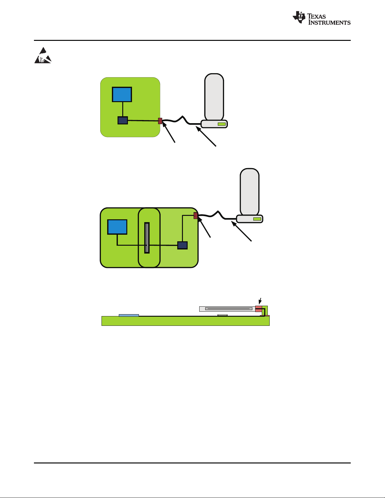
RX1P [1]
CTRL
RT
RT
VBB= 1.7 V TYP
V
BB
RT
RT
Equalizer
Equalizer
Driver
Driver
OOB
Detect
OOB
Detect
SN75LVCP601
TX1P [15]
RX1N [2]
TX1N [14]
RX2N [12]
RX2P [11]
TX2N [4]
TX2P [5]
EN[7]
DE2[8]
DE1[9]
VCC[10,20]
GND[3,13,18]
EQ1[17]
EQ2[19]
DEW1 [16]
DEW2 [6]
SN75LVCP601
www.ti.com
SLLSE41B –JUNE 2010– REVISED FEBRUARY 2012
Figure 2. Data Flow Block Diagram
NAME PIN DESCRIPTION NAME PIN DESCRIPTION
RX1P 1 Input 1, non-inverting RX2P 11 Input 2, non-inverting
RX1N 2 Input 1, inverting RX2N 12 Input 2, inverting
GND 3 Ground GND 13 Ground
TX2N 4 Output 2, inverting TX1N 14 Output 1, inverting
TX2P 5 Output 2, non-inverting TX1P 15 Output 1, non-inverting
(1)
DEW2
(1)
EN
(2)
DE2
(2)
DE1
Vcc 10 3.3-V supply Vcc 20 3.3-V supply
(1) DEW1/2, EN tied to Vcc via internal PU resistor
(2) DE1, DE2, EQ1, EQ2 are tied to Vcc/2 via internal resistor
6 De-emphasis width cntrl.-CH 2 DEW1
7 Enable EQ1
8 De-emphasis CH2 GND 18 Ground
9 De-emphasis CH1 EQ2
PIN TABLE
(1)
(2)
(2)
16 De-emphasis width cntrl.-CH 1
17 EQ control CH 1
19 EQ control CH 2
Copyright © 2010–2012, Texas Instruments Incorporated 3
Page 4
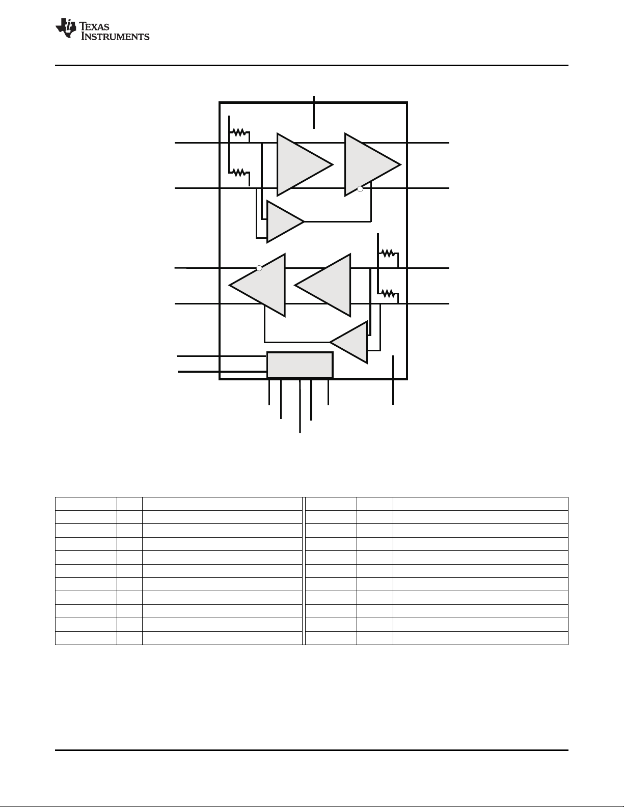
20
19
18
17
16
6
7
8
9
10
15
14
13
12
11
1
2
3
4
5
RX1P
RX1N
GND
TX2 N
TX2 P
VCC
EN
DE 2
DE 1
DEW 2
RX2P
RX2N
GND
TX1 N
TX1 P
EQ 2
EQ 1
VCC
DEW 1
GND
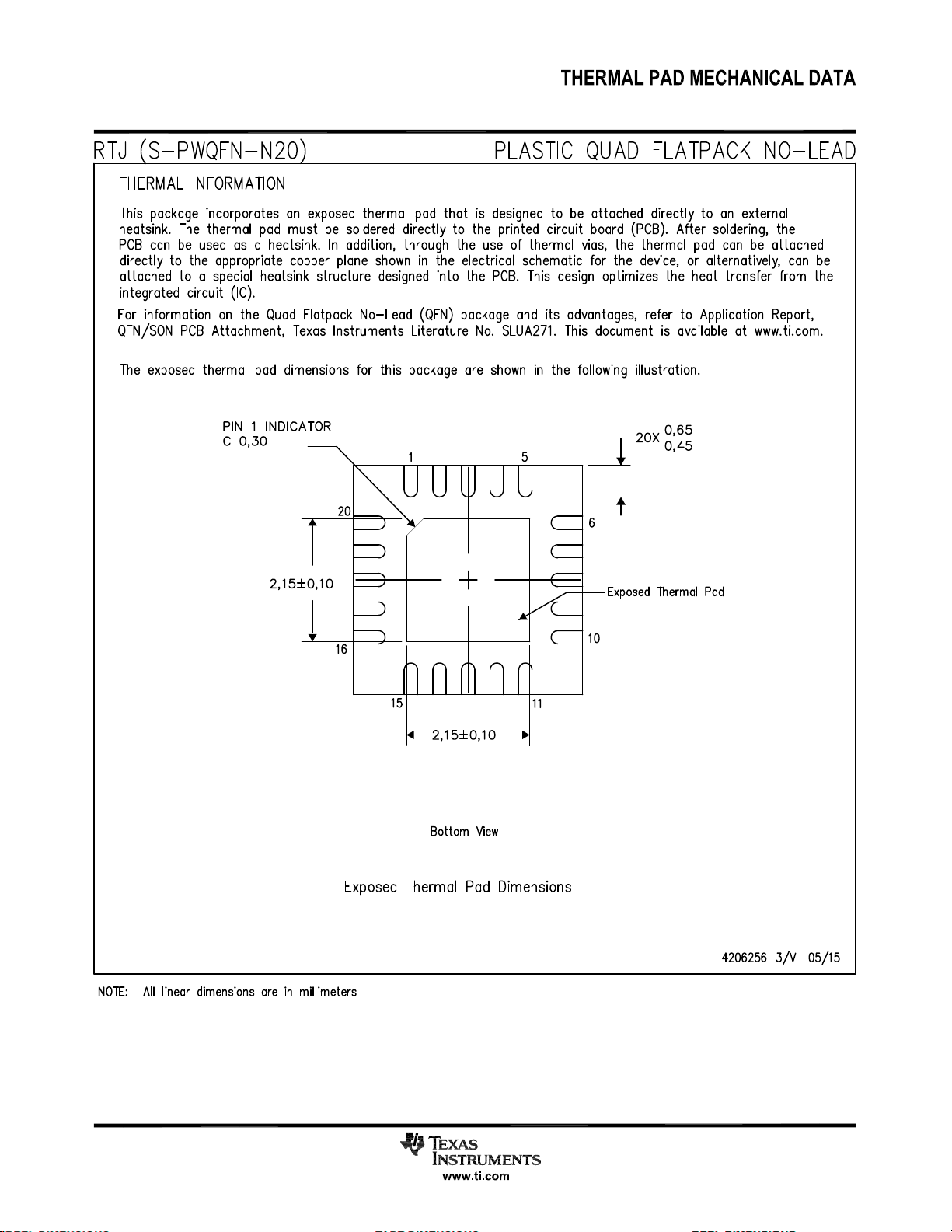
LVCP601RTJ
Thermal Pad must
be soldered to PCB
GND plane for
efficient thermal
performance
Bottom View
1
1
1
2
1
RX1P
RX1N
GND
TX2 N
TX2 P
DEW 2
DE 1
DE 2
EN
VCC
RX2P
RX2N
GND
TX1 N
TX1 P
VCC
DEW 1
EQ 2
EQ 1
GND
LVCP601RTJ
Top View
18
19
20
10
9
8
7
6
1
2
3
4
5
16
17
11
12
13
14
15
SN75LVCP601
SLLSE41B –JUNE 2010– REVISED FEBRUARY 2012
www.ti.com
PACKAGE PINOUT
PIN FUNCTIONS
PIN
NO. NAME
HIGH-SPEED DIFFERENTIAL I/O
2 RX1N I, CML
1 RX1P I, CML
12 RX2N I, CML
11 RX2P I, CML
14 TX1N O, VML
15 TX1P O, VML
4 TX2N O, VML
5 TX2P O, VML
CONTROL PINS
7 EN I, LVCMOS Device enable/disable pin, internally pulled to VCC. See Table 2.
8, 9 DE1, DE2
17, 19 EQ1, EQ2
16, 6 DEW1, DEW2 I, LVCMOS De-emphasis width control for CH 1 and CH 2. See Table 2.
POWER
10, 20 Vcc Power Positive supply should be 3.3 V ± 10%.
3, 13, 18 GND Power Supply ground
(1) Internally biased to Vcc/2 with >200-kΩ pullup/pulldown. When 3-state pins are left as NC, board leakage at the pin pad must be <1 µA;
otherwise, drive to Vcc/2 to assert mid-level state.
(1)
(1)
PIN TYPE DESCRIPTION
Non-inverting and inverting CML differential input for CH 1 and CH 2. These pins are
tied to an internal voltage bias by a dual-termination resistor circuit.
Non-inverting and inverting VML differential output for CH 1 and CH 2. These pins are
internally tied to voltage bias by termination resistors.
I, LVCMOS Selects de-emphasis settings for CH 1 and CH 2 per Table 1. Internally tied to VCC/2
I, LVCMOS Selects equalization settings for CH 1 and CH 2 per Table 1. Internally tied to VCC/2
4 Copyright © 2010–2012, Texas Instruments Incorporated
Page 5
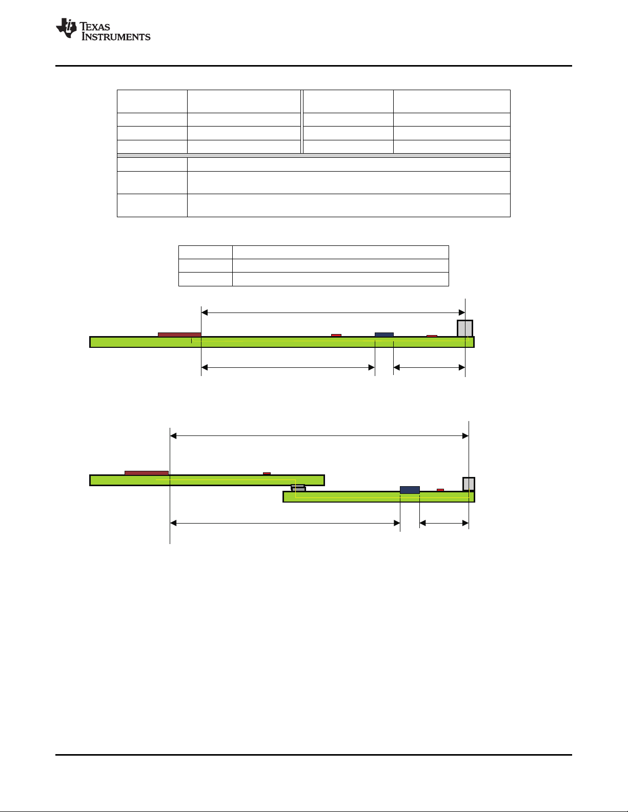
16 in. (40.6 cm)
24 in. (61 cm)
SATA Host
Redriver
Redriver on Motherboard
Main Board
SATA Host
Redriver
Dock Board
Redriver on Dock Board
SATA
Connector
SATA
Connector
16 in. (40.6 cm)
8 in.
(20.3 cm)
8 in.
(20.3 cm)
24 in. (61 cm)
SN75LVCP601
www.ti.com
SLLSE41B –JUNE 2010– REVISED FEBRUARY 2012
Table 1. Tx/Rx EQ and DE Pulse-Duration Settings
DE1/DE2 EQ1/EQ2
NC (default) –4 NC (default) 0
0 0 0 7
1 –2 1 14
DEW1/DEW2 Device Function → DE Width for CH1/CH2
0 De-emphasis pulse duration, short (recommended setting when link operates at SATA
1 (default) De-emphasis pulse duration, long (recommended setting when link operates at SATA
CH1/CH2De-Emphasis CH1/CH2Equalization
dB (at 6Gbps) dB (at 6Gbps)
1.5/3/6 Gbps)
1.5/3 Gbps speed only)
Table 2. Control Pin Settings
EN Device Function → Standby Mode
0 Device in standby mode
1 (default) Device enabled
NOTE: *Trace lengths are suggested values based on TI spice simulations (done over programmable limits of input EQ and
Copyright © 2010–2012, Texas Instruments Incorporated 5
output de-emphasis) to meet SATA loss and jitter spec.
Actual trace length supported by the LVCP601 may be more or less than suggested values and depends on board
layout, trace widths, and number of connectors used in the SATA signal path.
Figure 3. Trace Length Example* for LVCP601
Page 6
15
14
13
12
11
1
2
3
4
5
3.3 V
LVCP601 RTJ
RX1P
RX1N
TX2N
TX2P
TX1P
TX1N
RX2N
RX2P
10 nF
10 nF
10 nF
10 nF
10 nF
10 nF
10 nF
10 nF
EQ2
EQ1
DEW1
20
19
18
17
16
6
7
8
9
10
1.0 Fm
1.0 Fm
1.0 Fm
SATA Host
SATA
Connector
DEW2
EN
DE1
DE2
Vcc
Vcc
SN75LVCP601
SLLSE41B –JUNE 2010– REVISED FEBRUARY 2012
(1) Place supply capacitors close to device pin.
(2) EN can be left open or tied to supply when no external control is implemented.
(3) Output de-emphasis selection is set at –2 dB, EQ at 7 dB, and DE duration for SATA I/II/III operation for both
channels.
(4) Actual EQ/DE duration settings depend on device placement relative to host and SATA connector.
Figure 4. Typical Device Implementation
www.ti.com
OPERATION DESCRIPTION
INPUT EQUALIZATION
Each differential input of the SN75LVCP601 has programmable equalization in its front stage. The equalization
setting is shown in Table 1. The input equalizer is designed to recover a signal even when no eye is present at
the receiver, and effectively supports FR4 trace at the input anywhere from 4 in. (10.2 cm) to 20 in. (50.8 cm) at
SATA 6G speed.
OUTPUT DE-EMPHASIS
The SN75LVCP601 provides the de-emphasis settings shown in Table 1. De-emphasis is controlled
independently for each channel, and is set by the control pins DE1 and DE2 as shown in Table 1. There are two
de-emphasis duration settings available in the device. DEW1 and DEW2 control the DE durations for channels
one and two, respectively. The recommended settings for these control pins are listed Table 1. Output
de-emphasis is capable of supporting FR4 trace at the output anywhere from 2 in. (5.1 cm) to 12 in. (30.5 cm) at
SATA 3G/6G speed.
LOW-POWER MODE
Two low-power modes are supported by the SN75LVCP601, listed as follows:
1. Standby mode (triggered by the EN pin, EN = 0 V)
– Low-power mode is controlled by the enable (EN) pin. In its default state, this pin is internally pulled high.
Pulling this pin LOW puts the device in standby mode within 2 µs (max). In this mode, all active
components of the device are driven to their quiescent level, and differential outputs are driven to Hi-Z
(open). Maximum power dissipation in this mode is 5 mW. Exiting from this mode to normal operation
requires a maximum latency of 5 µs.
6 Copyright © 2010–2012, Texas Instruments Incorporated
Page 7
SN75LVCP601
www.ti.com
SLLSE41B –JUNE 2010– REVISED FEBRUARY 2012
2. Auto low-power mode (triggered when a given channel is in the electrically idle state for more than 100 µs
and EN = Vcc)
– The device enters and exits low-power mode by actively monitoring the input signal (VIDp-p) level on
each of its channels independently. When the input signal on either or both channels is in the electrically
idle state, that is, VIDp-p < 50 mV and stays in this state for >100 µs, the associated channel(s) enters
into the low-power state. In this state, output of the associated channel(s) is driven to VCM and the
device selectively shuts off some circuitry to lower power by >80% of its normal operating power. Exit
time from the auto low-power mode is <50 ns.
Out-of-Band (OOB) SUPPORT
The squelch detector circuit within the device enables full detection of OOB signaling as specified in the SATA
specification. Differential signal amplitude at the receiver input of 50 mVpp or less is not detected as an activity
and hence not passed to the output. Differential signal amplitude of 150 mVp-p or more is detected as an activity
and therefore passed to the output, indicating activity. Squelch circuit ON/OFF time is 5 ns, maximum. While in
squelch mode, outputs are held to VCM.
DEVICE POWER
The SN75LVCP601 is designed to operate from a single 3.3 V supply. Always practice proper power-supply
sequencing procedure. Apply Vcc first, before any input signals are applied to the device. The power-down
sequence is in reverse order.
ABSOLUTE MAXIMUM RATINGS
over operating free-air temperature range (unless otherwise noted)
Supply voltage range
Voltage range Differential I/O –0.5 to 4 V
Electrostatic discharge Charged-device model
Continuous power dissipation See Thermal Table
(1) Stresses beyond those listed under Absolute Maximum Ratings may cause permanent damage to the device. These are stress ratings
only, and functional operation of the device at these or any conditions beyond those indicated under Recommended Operating
Conditions is not implied. Exposure to absolute-maximum-rated conditions for extended periods may affect device reliability.
(2) All voltage values, except differential voltages, are with respect to the network ground terminal.
(3) Tested in accordance with JEDEC Standard 22, Test Method A114-B.
(4) Tested in accordance with JEDEC Standard 22, Test Method C101-A.
(5) Tested in accordance with JEDEC Standard 22, Test Method A115-A.
(2)
V
CC
Control I/O –0.5 to Vcc + 0.5 V
Human-body model
Machine model
(3)
(4)
(5)
(1)
VALUE UNIT
–0.5 to 4 V
±10,000 V
±1500 V
±200 V
THERMAL INFORMATION
SN75LVCP601
THERMAL METRIC
θ
JA
θ
JCtop
θ
JB
(1) For more information about traditional and new thermal metrics, see the IC Package Thermal Metrics application report, SPRA953.
(2) The junction-to-ambient thermal resistance under natural convection is obtained in a simulation on a JEDEC-standard, high-K board, as
specified in JESD51-7, in an environment described in JESD51-2a.
(3) The junction-to-case (top) thermal resistance is obtained by simulating a cold plate test on the package top. No specific
JEDEC-standard test exists, but a close description can be found in the ANSI SEMI standard G30-88.
(4) The junction-to-board thermal resistance is obtained by simulating in an environment with a ring cold plate fixture to control the PCB
temperature, as described in JESD51-8.
Copyright © 2010–2012, Texas Instruments Incorporated Submit Documentation Feedback 7
Junction-to-ambient thermal resistance
Junction-to-case (top) thermal resistance
Junction-to-board thermal resistance
Product Folder Link(s): SN75LVCP601
(1)
(2)
(3)
(4)
QFN UNITS
20 PINS
38 °C/W
40 °C/W
10 °C/W
Page 8
SN75LVCP601
SLLSE41B –JUNE 2010– REVISED FEBRUARY 2012
www.ti.com
THERMAL INFORMATION (continued)
SN75LVCP601
THERMAL METRIC
(1)
QFN UNITS
20 PINS
ψ
ψ
θ
P
P
JT
JB
JCbot
D
SD
Junction-to-top characterization parameter
Junction-to-board characterization parameter
Junction-to-case (bottom) thermal resistance
Device power dissipation in active mode 215 to 288 mW
Device power dissipation under standby mode 5 mW
(5)
(6)
(7)
0.5 °C/W
0.9 °C/W
15.2 °C/W
(5) The junction-to-top characterization parameter, ψJT, estimates the junction temperature of a device in a real system and is extracted
from the simulation data for obtaining θJA, using a procedure described in JESD51-2a (sections 6 and 7).
(6) The junction-to-board characterization parameter, ψJB, estimates the junction temperature of a device in a real system and is extracted
from the simulation data for obtaining θJA, using a procedure described in JESD51-2a (sections 6 and 7).
(7) The junction-to-case (bottom) thermal resistance is obtained by simulating a cold plate test on the exposed (power) pad. No specific
JEDEC standard test exists, but a close description can be found in the ANSI SEMI standard G30-88.
RECOMMENDED OPERATING CONDITIONS
(Typical values for all parameters are at VCC= 3.3V and TA= 25°C. All temp limits are specified by design)
PARAMETER CONDITIONS MIN TYP MAX UNITS
V
CC
C
COUPLING
Supply voltage 3 3.3 3.6 V
Coupling capacitor 12 nF
Operating free-air temperature 0 85 °C
ELECTRICAL CHARACTERISTICS
over operating free-air temperature range (unless otherwise noted)
PARAMETER TEST CONDITIONS MIN TYP MAX UNIT
DEVICE PARAMETERS
P
D
P
SD
I
CC
I
CC_ALP
I
CC_STDBY
t
PDelay
AutoLP
AutoLP
t
ENB
t
DIS
ENTRY
EXIT
Power dissipation in active mode 215 288 mW
Power dissipation in standby EN = 0 V, DEWx = EQx = DEx = NC, K28.5
mode pattern at 6 Gbps, VID= 700 mV
Active-mode supply current 65 80 mA
Acive power-save mode I
CC
Standby mode supply current EN = 0 V 1 mA
Maximum data rate 1 6 Gbps
Propagation delay Measured using K28.5 pattern. See Figure 8. 323 400 ps
Auto low-power entry time Electrical idle at input; see Figure 9. 80 105 130 µs
Auto low-power exit time After first signal activity; see Figure 9. 42 50 ns
Device enable time EN 0→1 5 µs
Device disable time EN 1→0 2 µs
DEWx = EN = Vcc, EQx = DEx = NC, K28.5
pattern at 6 Gbps, VID= 700 mV
EN = 3.3 V, DEWx= 0 V, EQx/DEx = NC,
K28.5 pattern at 6 Gbps, VID= 700 mV
When device is enabled and auto low-power
conditions are met
p-p
p-p
5 mW
p-p
6.5 10 mA
8 Submit Documentation Feedback Copyright © 2010–2012, Texas Instruments Incorporated
Product Folder Link(s): SN75LVCP601
Page 9

SN75LVCP601
www.ti.com
ELECTRICAL CHARACTERISTICS (continued)
over operating free-air temperature range (unless otherwise noted)
PARAMETER TEST CONDITIONS MIN TYP MAX UNIT
OUT-OF-BAND (OOB)
V
OOB
D
VdiffOOB
D
VCMOOB
t
OOB1
t
OOB2
CONTROL LOGIC
V
IH
V
IL
VIN
HYS
I
IH
I
IL
RECEIVER AC/DC
Z
DIFFRX
Z
SERX
VCM
RX
RL
DiffRX
RX
DiffRLSlope
RL
CMRX
V
diffRX
IB
RX
t
20-80RX
t
skewRX
Input OOB threshold f = 750 MHz 50 78 150 mVpp
OOB differential delta 25 mV
OOB common-mode delta 50 mV
OOB mode enter See Figure 9. 3 5 ns
OOB mode exit 3 5 ns
Input high voltage For all control pins 1.4 V
Input low voltage 0.5 V
Input hysteresis 115 mV
High-level input current µA
Low-level input current µA
EQx, DEx = Vcc 30
EN, DEWx = Vcc 1
EQx, DEx = GND –30
EN, DEWx = GND –10
Differential-input impedance 85 100 115 Ω
Single-ended input impedance 40 Ω
Common-mode voltage 1.8 V
f = 150 MHz–300 MHz 18 28
f = 300 MHz–600 MHz 14 17
Differential-mode return loss (RL) f = 600 MHz–1.2 GHz 10 12 dB
f = 1.2 GHz–2.4 GHz 8 9
f = 2.4 GHz–3 GHz 3 9
Differential-mode RL slope f = 300 MHz–6 GHz (See Figure 5.) –13 dB/dec
f = 150 MHz–300 MHz 5 10
f = 300 MHz–600 MHz 5 17
Common-mode return loss f = 600 MHz–1.2 GHz 2 23 dB
f = 1.2 GHz–2.4 GHz 1 16
f = 2.4 GHz–3 GHz 1 12
Differential input voltage PP f = 1.5 GHz and 3 GHz 120 1600 mVppd
f = 150 MHz–300 MHz 30 41
f = 300 MHz–600 MHz 30 38
f = 600 MHz–1.2 GHz 20 32
Impedance balance f = 1.2 GHz–2.4 GHz 10 26 dB
f = 2.4 GHz–3 GHz 10 25
f = 3 GHz–5 GHz 4 20
f = 5 GHz–6.5 GHz 4 17
Rise times and fall times measured between
Rise/fall time 62 75 ps
20% and 80% of the signal. SATA 6-Gbps
speed measured 1 in, (2.5 cm) from device
pin
Difference between the single-ended
Differential skew 30 ps
midpoint of the RX+ signal rising/falling edge,
and the single-ended midpoint of the RX–
signal falling/rising edge
SLLSE41B –JUNE 2010– REVISED FEBRUARY 2012
Copyright © 2010–2012, Texas Instruments Incorporated Submit Documentation Feedback 9
Product Folder Link(s): SN75LVCP601
Page 10
SN75LVCP601
SLLSE41B –JUNE 2010– REVISED FEBRUARY 2012
www.ti.com
ELECTRICAL CHARACTERISTICS (continued)
over operating free-air temperature range (unless otherwise noted)
PARAMETER TEST CONDITIONS MIN TYP MAX UNIT
TRANSMITTER AC/DC
Z
diffTX
Z
SETX
V
TXtrans
RL
DiffTX
TX
DiffRLSlope
RL
CMTX
IB
TX
Diff
VppTX
DE Output de-emphasis f = 3 GHz, DE1/DE2 = 1 –2 dB
t
DE
VCM
AC_TX
VCM
TX
t
20-80TX
t
skewTX
TxR/F
Imb
TxAmp
Imb
Pair differential impedance 85 100 122 Ω
Single-ended impedance 40 Ω
Sequencing transient voltage –1.2 1.2 V
Transient voltages on the serial data bus
during power sequencing (lab load)
f = 150 MHz–300 MHz 14 24
f = 300 MHz–600 MHz 8 19
Differential-mode return loss f = 600 MHz–1.2 GHz 6 14 dB
f = 1.2 GHz–2.4 GHz 6 10
f = 2.4 GHz–3 GHz 3 10
Differential-mode RL slope f = 300 MHz–3 GHz (SeeFigure 5.) –13 dB/dec
f = 150 MHz–300 MHz 5 20
f = 300 MHz–600 MHz 5 19
Common-mode return loss f = 600 MHz–1.2 GHz 2 17 dB
f = 1.2 GHz–2.4 GHz 1 12
f = 2.4 GHz–3.0 GHz 1 11
f = 150 MHz–300 MHz 30 41
f = 300 MHz–600 MHz 30 38
f = 600 MHz–1.2 GHz 20 33
Impedance balance f = 1.2 GHz–2.4 GHz 10 24 dB
f = 2.4 GHz–3 GHz 10 26
f = 3 GHz–5 GHz 4 22
f = 5 GHz–6.5 GHz 4 21
Differential output-voltage swing 550 mVppd
f = 3 GHz, DE1/DE2 = 0, DEWx = NC,
(under no interconnect loss)
f = 3 GHz, DE1/DE2 = 0 0
f = 3 GHz, DE1/DE2 = NC –4
De-emphasis duration ps
DEWx = 0 94
DEWx = 1 215
At 1.5 GHz 20 50 mVppd
TX AC CM voltage At 3 GHz 12 26
dBmV
At 6 GHz 13 30
Common-mode voltage 1.8 V
Rise times and fall times measured between
Rise/fall time 20% and 80% of the signal. At 6Gbps under 42 55 75 ps
no load conditions
Difference between the single-ended
Differential skew 6 20 ps
mid-point of the TX+ signal rising/falling
edge, and the single-ended mid-point of the
TX- signal falling/rising edge.
TX rise-fall imbalance At 3 Gbps 6% 20%
TX amplitude imbalance 2% 10%
(rms)
10 Submit Documentation Feedback Copyright © 2010–2012, Texas Instruments Incorporated
Product Folder Link(s): SN75LVCP601
Page 11

12" 6mil
Stripline
Jitter
Measurement
1
2
8" 6 milStripline
AWG*
AWG*
Jitter
Measurement
CP
CP = Compliancepoint
CP
SN75LVCP601
www.ti.com
SLLSE41B –JUNE 2010– REVISED FEBRUARY 2012
ELECTRICAL CHARACTERISTICS (continued)
over operating free-air temperature range (unless otherwise noted)
PARAMETER TEST CONDITIONS MIN TYP MAX UNIT
TRANSMITTER JITTER
DJ
TX
RJ
TX
DJ
TX
RJ
TX
(1) TJ = (14.1 × RJSD+ DJ), where RJSDis one standard deviation value of RJ Gaussian distribution. Jitter measurement is at the SATA
connector and includes jitter generated at the package connection on the printed circuit board, and at the board interconnect as shown
in Figure 6.
Deterministic jitter
Figure 6
Residual random jitter
Deterministic jitter
Figure 6
Residual random jitter
(1)
at CP in
(1)
at CP in
(1)
(1)
VID = 500 mVpp, UI = 333 ps,
K28.5 control character
VID = 500 mVpp, UI = 333 ps,
K28.7 control character
VID = 500 mVpp, UI = 167 ps,
K28.5 control character
VID = 500 mVpp, UI = 167 ps,
K28.7 control character
0.06 0.19 UIp-p
0.01 2 ps-rms
0.08 0.34 UIp-p
0.09 2 ps-rms
Figure 5. TX, RX Differential Return Loss Limits
Figure 6. Jitter Measurement Test Condition
Copyright © 2010–2012, Texas Instruments Incorporated Submit Documentation Feedback 11
Product Folder Link(s): SN75LVCP601
Page 12
t
PDelay
t
PDelay
IN
OUT
t
OOB2
t
OOB1
Vcm
IN+
IN-
OUT+
OUT-
Vcm
50 mV
t
OOB1
VCM
RX
VCM
TX
AutoLP
ENTRY
AutoLP
EXIT
RX1,2P
RX1,2N
TX1,2P
TX1,2N
PowerSaving
Mode
SN75LVCP601
SLLSE41B –JUNE 2010– REVISED FEBRUARY 2012
Figure 7. Propagation Delay Timing Diagram
www.ti.com
Figure 8. OOB Enter and Exit Timing
Figure 9. Auto Low-Power Mode Enter and Exit Timing
12 Submit Documentation Feedback Copyright © 2010–2012, Texas Instruments Incorporated
Product Folder Link(s): SN75LVCP601
Page 13
1-bit 1 toNbits
1-bit
1 toNbits
Diff
VppTX
Diff
VppTX_DE
t
DE
t
DE
0 dB
-2 dB
-4 dB
LVCP601
Agilent
DCA -J
Agilent
ParBERT
With LVCP601
Without LVCP601
TP1
TP2
TP3
TP4
TP1 TP4
EQ = 14 dB
DE = –2 dB
Agilent
ParBERT
Agilent
DCA -J
16-in., 4-mil (40.6-cm, 0.101-mm)
FR4 Trace +
2-in., 9.5-mil (5.05-cm, 0.241-mm)
FR4 Trace
8-in., 4-mil (20.3-cm, 0.101-mm)
FR4 Trace +
2-in., 9.5-mil (5.05-cm, 0.241-mm)
FR4 Trace
16-in., 4-mil (40.6-cm, 0.101-mm) FR4 Trace +
8-in., 4-mil (20.3-cm, 0.101-mm) FR4 Trace
4-in., 9.5-mil (10.1-cm, 0.241-mm) FR4 Trace +
SN75LVCP601
www.ti.com
Figure 10. TX Differential Output De-Emphasis
SN75LVCP601 TYPICAL PERFORMANCE CURVE
• Input signal characteristics
– Data rate = 6 Gbps, 3 Gbps, 1.5 Gbps
– Amplitude = 500 mVp-p
– Data pattern = K28.5
• SN75LVCP601 device setup
– Temperature = 25°C
– Voltage = 3.3 V
– De-emphasis duration = 117 ps (short)
– Equalization and de-emphasis set to optimize performance at 6 Gbps
SLLSE41B –JUNE 2010– REVISED FEBRUARY 2012
Copyright © 2010–2012, Texas Instruments Incorporated Submit Documentation Feedback 13
Figure 11. Performance Curve Measurement Setup
Product Folder Link(s): SN75LVCP601
Page 14

13.24101165.42.0029.856.7TP4
Without
LVCP601
459.62149.7557.11.9212.739.0TP4
With
LVCP601
623.02141.3788.81.9115.942.0TP3
81.2428.92401.9365.491.8TP2
350.52159.2412.41.883.329.0TP1
Eye
Diagram
Eye
Opening
mV
Eye
Width
ps
Eye
Amplitude
mV
RJ
(rms)
ps
DJ
(δ-δ)
ps
TJ
(1e-12)
ps
TestPoint
122.26118258.81.96101.8128.6TP4
Without
LVCP601
463.42305.0615.31.9920.347.9TP4
With
LVCP601
611.62321714.51.9612.839.6TP3
222.36237314.91.8946.872.7TP2
392.84326430.91.893.829.7TP1
Eye
Diagram
Eye
Opening
mV
Eye
Width
ps
Eye
Amplitude
mV
RJ
(rms)
ps
DJ
(δ-δ)
ps
TJ
(1e-12)
ps
TestPoint
SN75LVCP601
SLLSE41B –JUNE 2010– REVISED FEBRUARY 2012
SN75LVCP601 TYPICAL PERFORMANCE CURVE (continued)
www.ti.com
Figure 12. Jitter and VOD Results: Case 1 at 6 Gbps
Figure 13. Jitter and VOD Results: Case 2 at 3 Gbps
14 Submit Documentation Feedback Copyright © 2010–2012, Texas Instruments Incorporated
Product Folder Link(s): SN75LVCP601
Page 15

217.46493322.82.3081.9113.3TP4
Without
LVCP601
442.42632.0672.82.6221.557.3TP4
With
LVCP601
604.02649753.12.3113.244.9TP3
318.48589363.42.1138.667.5TP2
417.286594482.263.434.3TP1
Eye
Diagram
Eye
Opening
mV
Eye
Width
ps
Eye
Amplitude
mV
RJ
(rms)
ps
DJ
(δ-δ)
ps
TJ
(1e-12)
ps
TestPoint
Input Trace Length (in)
Residual DJ (ps)
Eye Opening (V)
2 4 6 8 10 12 14 16 18 20 22
0 0.1
2 0.2
4 0.3
6 0.4
8 0.5
10 0.6
12 0.7
14 0.8
G001
Residual DJ 3Gbps
Residual DJ 6Gbps
Eye Opening 3Gbps
Eye Opening 6Gbps
SN75LVCP601
www.ti.com
SLLSE41B –JUNE 2010– REVISED FEBRUARY 2012
SN75LVCP601 TYPICAL PERFORMANCE CURVE (continued)
Figure 14. Jitter and VOD Results: Case 3 at 1.5 Gbps
TYPICAL CHARACTERISTICS
RESIDUAL DJ AND EYE OPENING
vs
INPUT TRACE LENGTH
Copyright © 2010–2012, Texas Instruments Incorporated Submit Documentation Feedback 15
Product Folder Link(s): SN75LVCP601
Figure 15.
Page 16

Output Trace Length (in)
Residual DJ (ps)
Eye Opening (V)
2 4 6 8 10 12 14 16 18 20 22
0 0
5 0.1
10 0.2
15 0.3
20 0.4
25 0.5
30 0.6
35 0.7
40 0.8
G002
Residual DJ 3Gbps
Residual DJ 6Gbps
Eye Opening 3Gbps
Eye Opening 6Gbps
SN75LVCP601
SLLSE41B –JUNE 2010– REVISED FEBRUARY 2012
TYPICAL CHARACTERISTICS (continued)
www.ti.com
RESIDUAL DJ AND EYE OPENING
vs
OUTPUT TRACE LENGTH
Figure 16.
SPACER
REVISION HISTORY
Changes from Revision A (October 2011) to Revision B Page
• Changed pin type from CML to VML for pins 4, 5, 14, 15 .................................................................................................... 4
Changes from Original (June 2010) to Revision A Page
• Changed pin EN number From: 4 To: 7 ............................................................................................................................... 4
16 Submit Documentation Feedback Copyright © 2010–2012, Texas Instruments Incorporated
Product Folder Link(s): SN75LVCP601
Page 17
PACKAGE OPTION ADDENDUM
www.ti.com
30-Dec-2015
PACKAGING INFORMATION
Orderable Device Status
SN75LVCP601RTJR ACTIVE QFN RTJ 20 Green (RoHS
SN75LVCP601RTJT ACTIVE QFN RTJ 20 250 Green (RoHS
(1)
The marketing status values are defined as follows:
ACTIVE: Product device recommended for new designs.
LIFEBUY: TI has announced that the device will be discontinued, and a lifetime-buy period is in effect.
NRND: Not recommended for new designs. Device is in production to support existing customers, but TI does not recommend using this part in a new design.
PREVIEW: Device has been announced but is not in production. Samples may or may not be available.
OBSOLETE: TI has discontinued the production of the device.
Package Type Package
(1)
Drawing
Pins Package
Qty
Eco Plan
(2)
& no Sb/Br)
& no Sb/Br)
Lead/Ball Finish
(6)
CU NIPDAU | Call TI Level-2-260C-1 YEAR 0 to 85 LVC601
CU NIPDAU | Call TI Level-2-260C-1 YEAR 0 to 85 LVC601
MSL Peak Temp
(3)
Op Temp (°C) Device Marking
(4/5)
(2)
Eco Plan - The planned eco-friendly classification: Pb-Free (RoHS), Pb-Free (RoHS Exempt), or Green (RoHS & no Sb/Br) - please check http://www.ti.com/productcontent for the latest availability
information and additional product content details.
TBD: The Pb-Free/Green conversion plan has not been defined.
Pb-Free (RoHS): TI's terms "Lead-Free" or "Pb-Free" mean semiconductor products that are compatible with the current RoHS requirements for all 6 substances, including the requirement that
lead not exceed 0.1% by weight in homogeneous materials. Where designed to be soldered at high temperatures, TI Pb-Free products are suitable for use in specified lead-free processes.
Pb-Free (RoHS Exempt): This component has a RoHS exemption for either 1) lead-based flip-chip solder bumps used between the die and package, or 2) lead-based die adhesive used between
the die and leadframe. The component is otherwise considered Pb-Free (RoHS compatible) as defined above.
Green (RoHS & no Sb/Br): TI defines "Green" to mean Pb-Free (RoHS compatible), and free of Bromine (Br) and Antimony (Sb) based flame retardants (Br or Sb do not exceed 0.1% by weight
in homogeneous material)
(3)
MSL, Peak Temp. - The Moisture Sensitivity Level rating according to the JEDEC industry standard classifications, and peak solder temperature.
(4)
There may be additional marking, which relates to the logo, the lot trace code information, or the environmental category on the device.
(5)
Multiple Device Markings will be inside parentheses. Only one Device Marking contained in parentheses and separated by a "~" will appear on a device. If a line is indented then it is a continuation
of the previous line and the two combined represent the entire Device Marking for that device.
(6)
Lead/Ball Finish - Orderable Devices may have multiple material finish options. Finish options are separated by a vertical ruled line. Lead/Ball Finish values may wrap to two lines if the finish
value exceeds the maximum column width.
Important Information and Disclaimer:The information provided on this page represents TI's knowledge and belief as of the date that it is provided. TI bases its knowledge and belief on information
provided by third parties, and makes no representation or warranty as to the accuracy of such information. Efforts are underway to better integrate information from third parties. TI has taken and
continues to take reasonable steps to provide representative and accurate information but may not have conducted destructive testing or chemical analysis on incoming materials and chemicals.
TI and TI suppliers consider certain information to be proprietary, and thus CAS numbers and other limited information may not be available for release.
Samples
Addendum-Page 1
Page 18

PACKAGE OPTION ADDENDUM
www.ti.com
In no event shall TI's liability arising out of such information exceed the total purchase price of the TI part(s) at issue in this document sold by TI to Customer on an annual basis.
30-Dec-2015
Addendum-Page 2
Page 19

PACKAGE MATERIALS INFORMATION
www.ti.com 14-Jul-2012
TAPE AND REEL INFORMATION
*All dimensions are nominal
Device Package
SN75LVCP601RTJR QFN RTJ 20 3000 330.0 12.4 4.25 4.25 1.15 8.0 12.0 Q2
SN75LVCP601RTJT QFN RTJ 20 250 180.0 12.4 4.25 4.25 1.15 8.0 12.0 Q2
Type
Package
Drawing
Pins SPQ Reel
Diameter
(mm)
Reel
Width
W1 (mm)
A0
(mm)B0(mm)K0(mm)P1(mm)W(mm)
Pin1
Quadrant
Pack Materials-Page 1
Page 20
PACKAGE MATERIALS INFORMATION
www.ti.com 14-Jul-2012
*All dimensions are nominal
Device Package Type Package Drawing Pins SPQ Length (mm) Width (mm) Height (mm)
SN75LVCP601RTJR QFN RTJ 20 3000 367.0 367.0 35.0
SN75LVCP601RTJT QFN RTJ 20 250 210.0 185.0 35.0
Pack Materials-Page 2
Page 21

Page 22
Page 23

Page 24

IMPORTANT NOTICE
Texas Instruments Incorporated and its subsidiaries (TI) reserve the right to make corrections, enhancements, improvements and other
changes to its semiconductor products and services per JESD46, latest issue, and to discontinue any product or service per JESD48, latest
issue. Buyers should obtain the latest relevant information before placing orders and should verify that such information is current and
complete. All semiconductor products (also referred to herein as “components”) are sold subject to TI’s terms and conditions of sale
supplied at the time of order acknowledgment.
TI warrants performance of its components to the specifications applicable at the time of sale, in accordance with the warranty in TI’s terms
and conditions of sale of semiconductor products. Testing and other quality control techniques are used to the extent TI deems necessary
to support this warranty. Except where mandated by applicable law, testing of all parameters of each component is not necessarily
performed.
TI assumes no liability for applications assistance or the design of Buyers’ products. Buyers are responsible for their products and
applications using TI components. To minimize the risks associated with Buyers’ products and applications, Buyers should provide
adequate design and operating safeguards.
TI does not warrant or represent that any license, either express or implied, is granted under any patent right, copyright, mask work right, or
other intellectual property right relating to any combination, machine, or process in which TI components or services are used. Information
published by TI regarding third-party products or services does not constitute a license to use such products or services or a warranty or
endorsement thereof. Use of such information may require a license from a third party under the patents or other intellectual property of the
third party, or a license from TI under the patents or other intellectual property of TI.
Reproduction of significant portions of TI information in TI data books or data sheets is permissible only if reproduction is without alteration
and is accompanied by all associated warranties, conditions, limitations, and notices. TI is not responsible or liable for such altered
documentation. Information of third parties may be subject to additional restrictions.
Resale of TI components or services with statements different from or beyond the parameters stated by TI for that component or service
voids all express and any implied warranties for the associated TI component or service and is an unfair and deceptive business practice.
TI is not responsible or liable for any such statements.
Buyer acknowledges and agrees that it is solely responsible for compliance with all legal, regulatory and safety-related requirements
concerning its products, and any use of TI components in its applications, notwithstanding any applications-related information or support
that may be provided by TI. Buyer represents and agrees that it has all the necessary expertise to create and implement safeguards which
anticipate dangerous consequences of failures, monitor failures and their consequences, lessen the likelihood of failures that might cause
harm and take appropriate remedial actions. Buyer will fully indemnify TI and its representatives against any damages arising out of the use
of any TI components in safety-critical applications.
In some cases, TI components may be promoted specifically to facilitate safety-related applications. With such components, TI’s goal is to
help enable customers to design and create their own end-product solutions that meet applicable functional safety standards and
requirements. Nonetheless, such components are subject to these terms.
No TI components are authorized for use in FDA Class III (or similar life-critical medical equipment) unless authorized officers of the parties
have executed a special agreement specifically governing such use.
Only those TI components which TI has specifically designated as military grade or “enhanced plastic” are designed and intended for use in
military/aerospace applications or environments. Buyer acknowledges and agrees that any military or aerospace use of TI components
which have not been so designated is solely at the Buyer's risk, and that Buyer is solely responsible for compliance with all legal and
regulatory requirements in connection with such use.
TI has specifically designated certain components as meeting ISO/TS16949 requirements, mainly for automotive use. In any case of use of
non-designated products, TI will not be responsible for any failure to meet ISO/TS16949.
Products Applications
Audio www.ti.com/audio Automotive and Transportation www.ti.com/automotive
Amplifiers amplifier.ti.com Communications and Telecom www.ti.com/communications
Data Converters dataconverter.ti.com Computers and Peripherals www.ti.com/computers
DLP® Products www.dlp.com Consumer Electronics www.ti.com/consumer-apps
DSP dsp.ti.com Energy and Lighting www.ti.com/energy
Clocks and Timers www.ti.com/clocks Industrial www.ti.com/industrial
Interface interface.ti.com Medical www.ti.com/medical
Logic logic.ti.com Security www.ti.com/security
Power Mgmt power.ti.com Space, Avionics and Defense www.ti.com/space-avionics-defense
Microcontrollers microcontroller.ti.com Video and Imaging www.ti.com/video
RFID www.ti-rfid.com
OMAP Applications Processors www.ti.com/omap TI E2E Community e2e.ti.com
Wireless Connectivity www.ti.com/wirelessconnectivity
Mailing Address: Texas Instruments, Post Office Box 655303, Dallas, Texas 75265
Copyright © 2015, Texas Instruments Incorporated
Page 25

 Loading...