

SN75LBC968
9-CHANNEL BUS TRANSCEIVER
WITH ACTIVE TERMINATION
SLLS179C – APRIL 1994 – REVISED JANUARY 1999
1
POST OFFICE BOX 655303 • DALLAS, TEXAS 75265
D
Nine Single-Ended SCSI Transceiver
Channels With Active Termination
D
Programmable Drivers Provide Active
Negation (Totem Pole) or Wired-OR (Open
Drain) Outputs
D
24-mA Current-Mode Active Termination
With Common Nine-Channel Bus Enable
D
Low Output Capacitance Presented to SCSI
Bus, 13.5 pF Typ
D
3.3 V Compatible Logic Inputs Provide
Bridge from 3 V Controllers to 5 V SCSI
Bus
D
Designed to Operate at 10-Million Data
Transfers Per Second (Fast-SCSI)
D
Controlled Driver Rise and Fall Times
5 ns Min
D
High-Receiver Input-Voltage Hysteresis
500 mV Typ
D
Receiver Input-Noise Pulse Filter
5 ns Typ
D
Each Driver and Receiver Meets ANSI
X3.131-1994 (SCSI-2) and the Proposed
SCSI-3 Standards
D
Power-Up/Power-Down Glitch Protection
D
High Impedance Driver With VCC at 0 V
description
The SN75LBC968 is a nine-channel transceiver
with active termination that drives and receives
the signals from the single-ended, parallel data
buses such as the Small Computer-Systems
Interface (SCSI) bus. The features of the line drivers, receivers, and active-termination circuits provide the
optimum signal-to-noise ratios for reliable data transmission. Integration of the termination and transceivers in
the LinBiCMOS process provides the necessary analog-circuit performance, has low quiescent power, and
reduces the capacitance presented to the bus over separate termination and I/O circuits.
The transceivers of the SN75LBC968 can be enabled to function as totem-pole or open-drain outputs. The
open-drain mode drives the wired-OR lines of SCSI (BSY, SEL, and RST) by inputting the data to the direction
control input DE/RE instead of the A input. When driving the data through the A input, the outputs become totem
poles and provide active signal negation for a higher voltage level on low-to-high signal transitions on heavily
loaded buses. In either mode, the turn-on and turn-off output transition times are limited to minimize crosstalk
through capacitive coupling to adjacent lines and RF emissions from the cable. The receivers are also designed
for optimum analog performance by precisely controlling the input-voltage thresholds, providing wide
input-voltage hysteresis and including an input-noise filter. These features significantly increase the likelihood
of detecting only the desired data signal and rejecting noise.
LinBiCMOS is a trademark of Texas Instruments Incorporated.
Copyright 1999, Texas Instruments Incorporated
PRODUCTION DATA information is current as of publication date.
Products conform to specifications per the terms of Texas Instruments
standard warranty. Production processing does not necessarily include
testing of all parameters.
1
2
3
4
5
6
7
8
9
10
11
12
13
14
15
16
17
18
19
20
21
22
23
24
25
26
27
28
56
55
54
53
52
51
50
49
48
47
46
45
44
43
42
41
40
39
38
37
36
35
34
33
32
31
30
29
GND
TE
GND
1A
1DE/RE
2A
2DE/RE
3A
3DE/RE
4A
4DE/RE
V
CC1
GND
GND
GND
GND
GND
V
CC
5A
5DE/RE
6A
6DE/RE
7A
7DE/RE
8A
8DE/RE
9A
9DE/RE
8B
GND
CE
NC
NC
NC
7B
NC
6B
NC
5B
V
CC
GND
GND
GND
GND
GND
V
CC
NC
4B
NC
3B
NC
2B
NC
1B
NC
9B
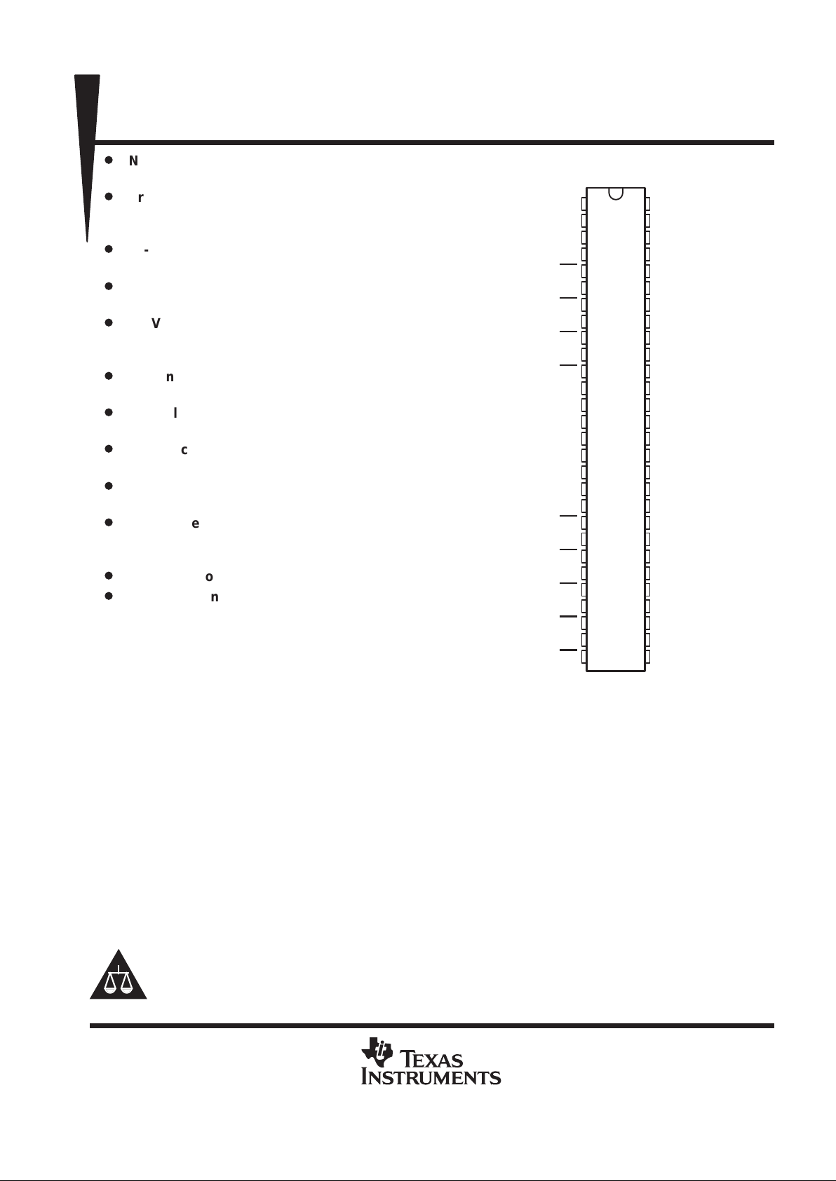
DL PACKAGE
(TOP VIEW)
NC – No internal connection
Please be aware that an important notice concerning availability, standard warranty, and use in critical applications of
Texas Instruments semiconductor products and disclaimers thereto appears at the end of this data sheet.
SN75LBC968
9-CHANNEL BUS TRANSCEIVER
WITH ACTIVE TERMINATION
SLLS179C – APRIL 1994 – REVISED JANUARY 1999
2
POST OFFICE BOX 655303 • DALLAS, TEXAS 75265
description (continued)
The communication between the SN75LBC968 and the controller can be accomplished at 3.3-V logic levels
provided that the V
CC1
input connects to the same supply rail as the controller. This provides a bridge from the
lower-voltage circuit and the 5-V SCSI bus. The SN75LBC968 also removes the need for special I/O buffers
(and associated power dissipation) on the controller itself. The SN75LBC968 must be used with a SCSI
controller with support for Differential SCSI.
The integrated, current-mode, active termination supplies a constant 24 mA of current (TERMPWR) to the bus
when the bus voltage falls below 2.5 V . This makes the next low-to-high (negation) signal transition independent
of the low-level (asserted) bus voltage, unlike voltage-mode terminators. The termination current is provided
through the TE input and from TERMPWR and can be disabled by letting the TE input float or by connecting
it to ground. The termination circuitry is independent from the line drivers and receivers and V
CC
or V
CC1
.
Operational termination is present as long as TERMPWR is applied.
The switching speeds of the SN75LBC968 are sufficient to transfer data over the data bus at ten million transfers
per second (Fast-SCSI). The specification, t
sk(lim)
, is for system skew budgeting and maintenance of bus set-up
and hold times. The device is available in the space-efficient shrink-small-outline package (SSOP) with 25-mil
lead pitch. The SN75LBC968 meets or exceeds the requirements of ANSI X3.131–1994 (SCSI-2) and the
proposed SPI (SCSI-3) standards, and is characterized for operation from 0°C to 70°C.
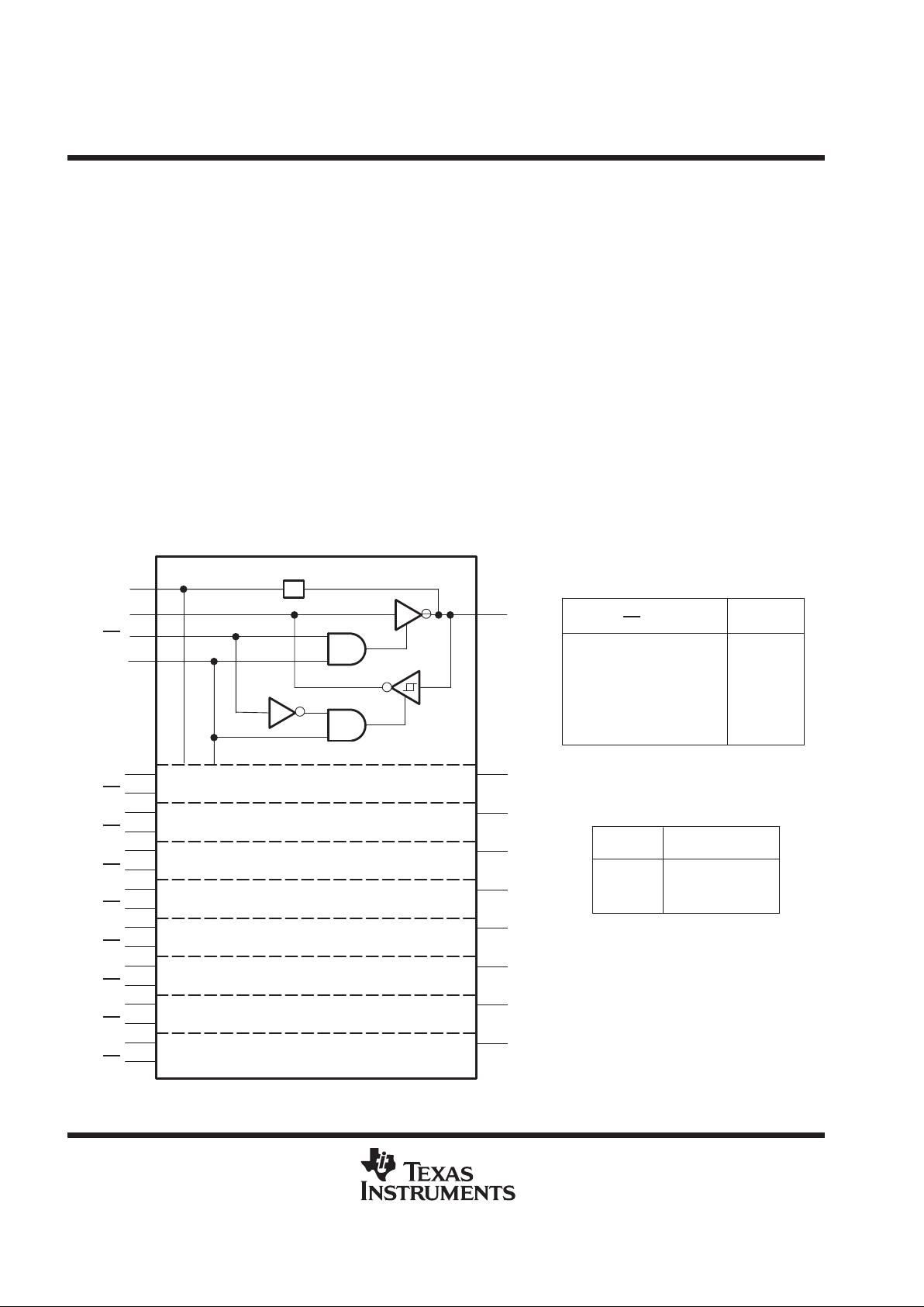
logic diagram (positive logic)
31
1B
56
37
35
33
2B
3B
4B
11
10
9
8
7
6
4
2
54
5
Channel 4
Channel 3
Channel 2
4DE/RE
4A
3DE/RE
3A
2DE/RE
2A
1A
TE
50
48
46
5B
6B
7B
24
23
22
21
20
19
Channel 7
Channel 6
Channel 5
7DE/RE
7A
6DE/RE
6A
5DE/RE
5A
29
8B
9B
28
27
26
25
Channel 9
Channel 8
9DE/RE
9A
8DE/RE
8A
CE
1DE/RE
Active Terminator
DE/RE BA
Z
H
L
Z
Z
H
Z
Z
Z
Z
H
L
Z
L
BA
INPUTS OUTPUTS
H = high level L = low level
X = irrelevant Z = high impedance
TERMINATION FUNCTION
OUTPUT
B
INPUT
TE
GND
V
TE
Open
Z
24-mA source
Z
CE
Function Tables
L
H
H
H
H
H
H
TRANSCEIVER FUNCTIONS
X
L
L
H
H
L
H
X
X
X
L
H
X
Open
X
L
H
X
X
Open
X
SN75LBC968
9-CHANNEL BUS TRANSCEIVER
WITH ACTIVE TERMINATION
SLLS179C – APRIL 1994 – REVISED JANUARY 1999
3
POST OFFICE BOX 655303 • DALLAS, TEXAS 75265
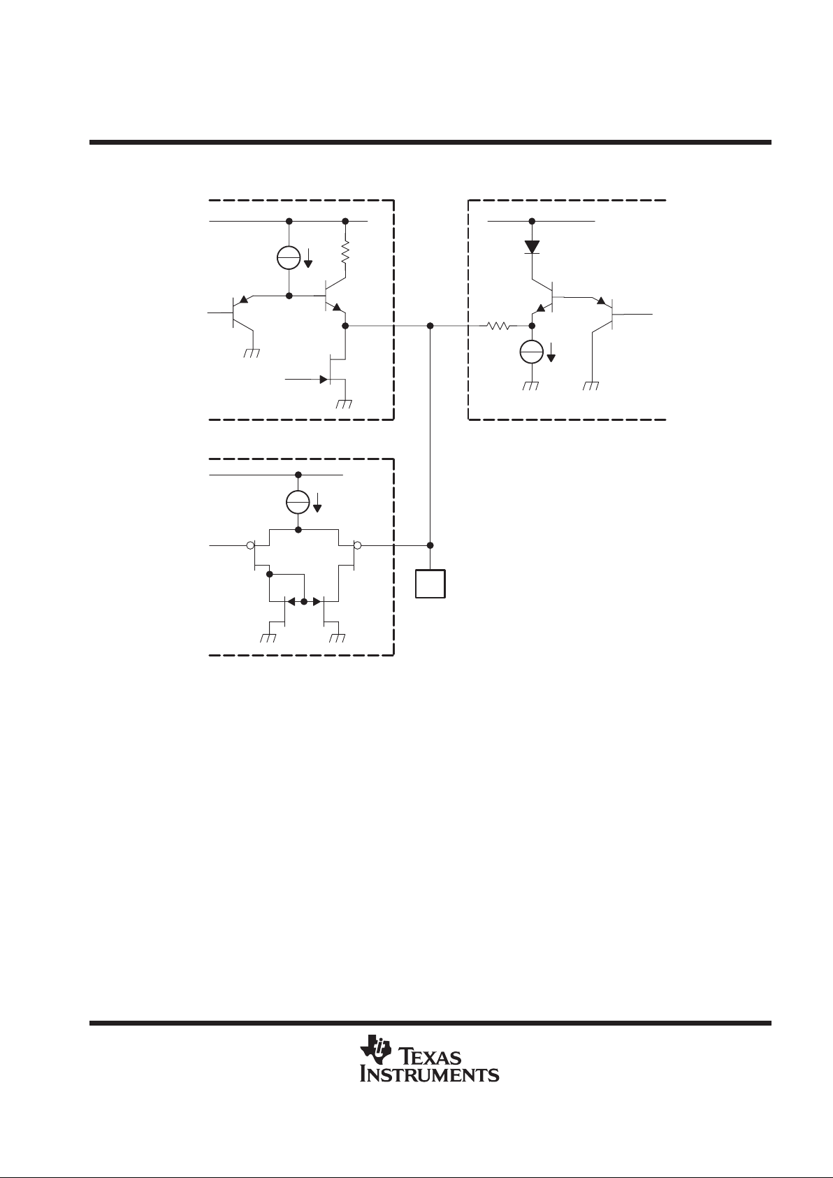
schematics
TEV
CC
DRIVER ACTIVE TERMINATOR
2.85 V
10 Ω
50 Ω
2.85 V
V
CC
V
ref
B
RECEIVER
absolute maximum ratings over operating free-air temperature range (unless otherwise noted)
†
Supply voltage range, V
CC
, V
CC1
, VTE (see Note 1) –0.5 V to 7 V. . . . . . . . . . . . . . . . . . . . . . . . . . . . . . . . . . .
Input voltage range, V
I
(A-side) V
CC1
+ 0.3 V. . . . . . . . . . . . . . . . . . . . . . . . . . . . . . . . . . . . . . . . . . . . . . . . . . . . . .
Bus voltage range (B-side) –0.5 V to 7 V. . . . . . . . . . . . . . . . . . . . . . . . . . . . . . . . . . . . . . . . . . . . . . . . . . . . . . . . .
Data I/O and control (A-side) voltage range –0.5 V to 7 V. . . . . . . . . . . . . . . . . . . . . . . . . . . . . . . . . . . . . . . . . . .
Continuous power dissipation (see Note 2) Internally Limited. . . . . . . . . . . . . . . . . . . . . . . . . . . . . . . . . . . . . . . . .
Operating free-air temperature range, T
A
0°C to 70°C. . . . . . . . . . . . . . . . . . . . . . . . . . . . . . . . . . . . . . . . . . . . . .
Storage temperature range, T
stg
65°C to 150°C. . . . . . . . . . . . . . . . . . . . . . . . . . . . . . . . . . . . . . . . . . . . . . . . . . . .
Lead temperature 1,6 mm (1/16 inch) from case for 10 seconds 260°C. . . . . . . . . . . . . . . . . . . . . . . . . . . . . . .
†
Stresses beyond those listed under “absolute maximum ratings” may cause permanent damage to the device. These are stress ratings only, and
functional operation of the device at these or any other conditions beyond those indicated under “recommended operating conditions” is not
implied. Exposure to absolute-maximum-rated conditions for extended periods may affect device reliability.
NOTES: 1. All voltage values are with respect to GND.
2. The maximum operating-junction temperature is internally limited. Use the dissipation rating table to operate below this temperature.

SN75LBC968
9-CHANNEL BUS TRANSCEIVER
WITH ACTIVE TERMINATION
SLLS179C – APRIL 1994 – REVISED JANUARY 1999
4
POST OFFICE BOX 655303 • DALLAS, TEXAS 75265
DISSIPATION RATING TABLE
PACKAGE
TA ≤ 25°C
POWER RATING
DERATING FACTOR
†
ABOVE TA = 25°C
TA = 70°C
POWER RATING
DL 2500 mW 20 mW/°C 1600 mW
†
Derating factors are the inverse of the junction-to-ambient thermal resistance when
board-mounted with no air flow .
recommended operating conditions
MIN NOM MAX UNIT
Supply voltage, V
CC
4.75 5 5.25 V
Supply voltage, V
CC1
(see Note 3) 3 5.25 V
Termination voltage, V
TE
4.25 5.25 V
High-level input voltage, V
IH
DE/RE, CE, A, B 2 V
Low-level input voltage, V
IL
DE/RE, CE, A, B 0.8 V
High-level output current, I
OH
A –8 mA
p
B 48
Low-level output current, I
OL
A 8
mA
Operating free-air temperature, T
A
0 70 °C
NOTE 3: All electrical characteristics are measured with V
CC1
= VCC unless otherwise noted.
driver electrical characteristics over recommended operating conditions (unless otherwise noted)
(see Figure 1)
PARAMETER TEST CONDITIONS MIN MAX UNIT
V
OH
High-level output voltage IOH = –20 mA 2 V
V
OL
Low-level output voltage IOL = 48 mA 0.5 V
I
IH
High-level input current VIH = 2 V, VCC = V
CC1
= 5.25 V –100 µA
I
IL
Low-level input current, A VIL = 0.5 V, VCC = V
CC1
= 5.25 V –100 µA
p
p
VO = 5.25 V , VCC = V
CC1
= 5.25 V –100
IOZHigh-impedance-state output current
VO = 0 V, VCC = V
CC1
= 5.25 V –100
µ
A
termination electrical characteristics over recommended operating conditions (unless otherwise
noted) (see Figure 2)
PARAMETER TEST CONDITIONS MIN TYP MAX UNIT
V
O(OC)
Open-circuit output voltage IO = 0 mA, VCC = V
CC1
= 0 V 2.5 2.85 3.24 V
VO = 0 V, VCC = V
CC1
= 0 V –24 mA
p
VO = 0.5 V, VCC = V
CC1
= 0 V –20 –24 mA
IOOutput current
VO = 3 V, VCC = V
CC1
= 0 V 100 µA
VO = 4 V, VCC = V
CC1
= 0 V 2 12 mA
SN75LBC968
9-CHANNEL BUS TRANSCEIVER
WITH ACTIVE TERMINATION
SLLS179C – APRIL 1994 – REVISED JANUARY 1999
5
POST OFFICE BOX 655303 • DALLAS, TEXAS 75265
receiver electrical characteristics over recommended operating conditions (unless otherwise
noted) (see Figure 3)
PARAMETER TEST CONDITIONS MIN TYP MAX UNIT
V
OH
High-level output voltage IOH = –8 mA 2 2.5 V
V
OL
Low-level output voltage IOL = 8 mA 0.8 V
V
IT+
Positive-going input threshold voltage
1.2 1.6 2 V
V
IT–
Negative-going input threshold voltage
V
CC
=
V
CC1
0.8 1.1 1.4 V
V
hys
Input hysteresis voltage (V
IT+
– V
IT–
) 0.2 0.5 V
I
IH
High-level input current VIH = 2 V 100 µA
I
IL
Low-level input current VIL = 0.5 V 100 µA
p
p
VO = 0 V –100
IOZHigh-impedance-state output current
VO = 5.25 V –100
µ
A
device electrical characteristics over recommended operating conditions (unless otherwise
noted)
PARAMETER TEST CONDITIONS MIN TYP†MAX UNIT
All drivers, receivers, and terminator
disabled
All inputs at 0 V 1.3 3
Supply current to V
All receivers enabled, termination and
drivers disabled, No load
CE at VCC,DE/RE at 0 V,
TE at 0 V
14 21
I
CC
y
CC
and V
CC1
All drivers enabled, termination and
DE/RE and CE at VCC,
A and TE at 0 V
33 45
mA
,
receivers disabled, No load
DE/RE and CE at VCC,
VTE = 0 V, A at V
CC1
15 21
I
CC
Supply current to TE
Termination and receivers enabled,
No load
TE at VTE,DE/RE at 0 V 33 45
CoBus port capacitance (see Note 4) 13.5 16.5 pF
I
IH
High-level input current DE/RE, CE VIH = VCC or 2 V 100 µA
I
IL
Low-level input current DE/RE, CE VIL = 0.5 V 100 µA
†
All typical values are at VCC = V
CC1
= 5 V, TA = 25°C.
NOTE 4: Tested in accordance with Annex G X3T9.2/855D, revision 14

SN75LBC968
9-CHANNEL BUS TRANSCEIVER
WITH ACTIVE TERMINATION
SLLS179C – APRIL 1994 – REVISED JANUARY 1999
6
POST OFFICE BOX 655303 • DALLAS, TEXAS 75265
driver switching characteristics over recommended operating conditions (unless otherwise
noted)
PARAMETER TEST CONDITIONS MIN TYP†MAX UNIT
t
PHL
Propagation delay time, high- to low-level output
(see Figure 4)
p
10 35 ns
t
PLH
Propagation delay time, low- to high-level output
(see Figure 4)
C
L
= 15
pF
15 45 ns
Skew limit
‡
,
the maximum delay time – minimum dela
y
VCC = V
CC1
= 5 V, TA = 25°C,
CL = 15 pF
14 ns
t
sk(lim)
Skew limit , the maximum delay time minimum delay
time
VCC = V
CC1
= 5 V, TA = 70°C,
CL = 15 pF
14 ns
t
sk(p)
Pulse skew, |t
PHL
– t
PLH
| VCC = V
CC1
= 5 V, TA = 25°C 8 ns
t
t
Output transition time, 10% to 90% or 90% to 10% of the
steady-state output
15 pF < CL < 100 pF 5 20 ns
Propagation delay time, low-level to high-impedance
From CE, CL = 15 pF 5 150
t
PLZ
gy, g
output (see Figure 5)
From DE/RE
,C
L
= 15 pF 45
ns
Propagation delay time, high-impedance to low-level
From CE, CL = 15 pF 5 150
t
PZL
gyg
output (see Figure 5)
From DE/RE,C
L
= 15 pF 45
ns
†
All typical values are at VCC = V
CC1
= 5 V, TA = 25°C.
‡
The value for this parameter was derived from the difference between the slowest and the fastest driver delay times measured on devices from
four sample wafer lots.
receiver switching characteristics over recommended of operating conditions (unless otherwise
noted)
PARAMETER TEST CONDITIONS MIN TYP†MAX UNIT
t
PHL
Propagation delay time, high- to low-level output
5 20 ns
t
PLH
Propagation delay time, low- to high-level output
See Figure 6
5 25 ns
Skew limit
‡
,
the maximum delay time – minimum dela
y
VCC = V
CC1
= 5 V, TA = 25°C,
See Figure 6
8.5 ns
t
sk(lim)
Skew limit , the maximum delay time minimum delay
time
VCC = V
CC1
= 5 V, TA = 70°C,
See Figure 6
8.5 ns
t
sk(p)
Pulse skew, |t
PHL
– t
PLH
|
VCC = V
CC1
= 5 V, TA = 25°C,
See Figure 6
6 ns
Propagation delay time, low-level to high-impedance
From CE, See Figure 7 5 150
t
PLZ
gy, g
output
From DE/RE
, See Figure 7 45
ns
Propagation delay time, high-impedance to low-level
From CE, See Figure 7 5 150
t
PZL
gy,g
output
From DE/RE
, See Figure 7 80
ns
Propagation delay time, high-level to high-impedance
From CE, See Figure 8 5 150
t
PHZ
gy,g g
output
From DE/RE
, See Figure 8 45
ns
Propagation delay time, high-impedance to high-level
From CE, See Figure 8 5 150
t
PZH
gy,g g
output
From DE/RE, See Figure 8 80
ns
†
All typical values are at VCC = V
CC1
= 5 V, TA = 25°C.
‡
The value for this parameter was derived from the difference between the slowest and the fastest driver delay times measured on devices from
four sample wafer lots.
thermal characteristics
PARAMETER TEST CONDITIONS MIN TYP MAX UNIT
R
θJA
Junction-to-free-air thermal resistance Board-mounted, no air flow 50 °C/W
R
θJC
Junction-to-case thermal resistance 12 °C/W
T
JS
Junction-shutdown temperature 180 °C

SN75LBC968
9-CHANNEL BUS TRANSCEIVER
WITH ACTIVE TERMINATION
SLLS179C – APRIL 1994 – REVISED JANUARY 1999
7
POST OFFICE BOX 655303 • DALLAS, TEXAS 75265
PARAMETER MEASUREMENT INFORMATION
CE
Termination
I
O
V
O
V
I
I
I
DE/RE
A
TE
To V
CC
To VCC or to
GND for I
OZ
B
Figure 1. Driver Test Circuit Currents and Voltages.
CE
Termination
I
O
V
O
V
TE
I
I
DE/RE
A
TE
B
Figure 2. Active Termination Voltages, Currents, and Test Circuit.
CE
Termination
I
O
V
O
V
O
I
I
DE/RE
B
TE
To GND
To VCC or to
GND for I
OZ
A
Figure 3. Receiver Voltages, Currents, and Test Circuit
NOTES: A. All input pulses are supplied by a generator having the following characteristics: tr 6 ns, tf 6 ns, PRR 1 MHz,
duty cycle = 50%, ZO = 50 Ω.
B. All resistances are in ohms and ±5%, unless otherwise indicated.
C. All capacitances are in picofarads and ±10%, unless otherwise indicated.
D. All indicated voltages are ±10 mV.

SN75LBC968
9-CHANNEL BUS TRANSCEIVER
WITH ACTIVE TERMINATION
SLLS179C – APRIL 1994 – REVISED JANUARY 1999
8
POST OFFICE BOX 655303 • DALLAS, TEXAS 75265
PARAMETER MEASUREMENT INFORMATION
CE
Termination
Output
DE/RE
A
TE
B
47 Ω
+
2.5 V
–
C
L
Inputs
V
CC
50%
0 V
V
CC
50%
0 V
V
CC
50%
V
OL
2.5 V
50%
V
OL
t
PHL
t
PLH
CE
DE/RE
A
B
NOTES: A. All input pulses are supplied by a generator having the following characteristics: tr 6 ns, tf 6 ns, PRR 1 MHz,
duty cycle = 50%, ZO = 50 Ω.
B. All resistances are in ohms and ±5%, unless otherwise indicated.
C. All capacitances are in picofarads and ±10%, unless otherwise indicated.
D. All indicated voltages are ±10 mV.
0 V
Figure 4. Driver Delay Time Test Circuit and Waveforms

SN75LBC968
9-CHANNEL BUS TRANSCEIVER
WITH ACTIVE TERMINATION
SLLS179C – APRIL 1994 – REVISED JANUARY 1999
9
POST OFFICE BOX 655303 • DALLAS, TEXAS 75265
CE
Termination
Output
DE/RE
A
TE
B
V
CC
560 Ω
47 Ω
+
2.5 V
–
C
L
Inputs
Input is Either
CE or DE/RE
V
CC
50%
0 V
V
CC
50%
0 V
V
CC
50%
V
OL
2.5 V
50%
V
OL
t
PLZ
t
PZL
CE
DE/RE
A
B
NOTES: A. All input pulses are supplied by a generator having the following characteristics: tr 6 ns, tf 6 ns, PRR 1 MHz,
duty cycle = 50%, ZO = 50 Ω.
B. All resistances are in ohms and ±5%, unless otherwise indicated.
C. All capacitances are in picofarads and ±10%, unless otherwise indicated.
D. All indicated voltages are ±10 mV.
Figure 5. Driver Delay Time Test Circuit and Waveforms

SN75LBC968
9-CHANNEL BUS TRANSCEIVER
WITH ACTIVE TERMINATION
SLLS179C – APRIL 1994 – REVISED JANUARY 1999
10
POST OFFICE BOX 655303 • DALLAS, TEXAS 75265
PARAMETER MEASUREMENT INFORMATION
CE
Termination
Output
DE/RE
B
TE
A
15 pF
V
CC
50%
0 V
V
OH
50%
V
OL
t
PLH
t
PHL
IN B
OUT A
50%
50%
Input
To V
CC
To GND
NOTES: A. All input pulses are supplied by a generator having the following characteristics: tr 6 ns, tf 6 ns, PRR 1 MHz,
duty cycle = 50%, ZO = 50 Ω.
B. All resistances are in ohms and ±5%, unless otherwise indicated.
C. All capacitances are in picofarads and ±10%, unless otherwise indicated.
D. All indicated voltages are ±10 mV.
Figure 6. Receiver Propagation Delay Time Test Circuit and Waveforms

SN75LBC968
9-CHANNEL BUS TRANSCEIVER
WITH ACTIVE TERMINATION
SLLS179C – APRIL 1994 – REVISED JANUARY 1999
11
POST OFFICE BOX 655303 • DALLAS, TEXAS 75265
PARAMETER MEASUREMENT INFORMATION
CE
Termination
Output
DE/RE
B
TE
A
V
CC
560 Ω
47 Ω
+
2.5 V
–
15 pF
Input is Either
CE or DE/RE
V
CC
50%
0 V
V
CC
50%
0 V
50%
V
OL
t
PLZ
t
PZL
CE
DE/RE
B
A
50%
50%
50%
15 pF
Inputs
NOTES: A. All input pulses are supplied by a generator having the following characteristics: tr 6 ns, tf 6 ns, PRR 1 MHz,
duty cycle = 50%, ZO = 50 Ω.
B. All resistances are in ohms and ±5%, unless otherwise indicated.
C. All capacitances are in picofarads and ±10%, unless otherwise indicated.
D. All indicated voltages are ±10 mV.
V
OH
Figure 7. Receiver Enable and Disable Times to and From Low-Level Output Test Circuit and Waveforms

SN75LBC968
9-CHANNEL BUS TRANSCEIVER
WITH ACTIVE TERMINATION
SLLS179C – APRIL 1994 – REVISED JANUARY 1999
12
POST OFFICE BOX 655303 • DALLAS, TEXAS 75265
PARAMETER MEASUREMENT INFORMATION
CE
Termination
Output
DE/RE
B
TE
A
GND
560 Ω
150 Ω
+
0 V
–
15 pF
Input is Either
CE or DE/RE
V
CC
50%
0 V
V
CC
50%
0 V
V
OH
50%
0 V
t
PHZ
t
PZH
CE
DE/RE
B
A
50%
50%
50%
15 pF
Inputs
NOTES: A. All input pulses are supplied by a generator having the following characteristics: tr 6 ns, tf 6 ns, PRR 1 MHz,
duty cycle = 50%, ZO = 50 Ω.
B. All resistances are in ohms and ±5%, unless otherwise indicated.
C. All capacitances are in picofarads and ±10%, unless otherwise indicated.
D. All indicated voltages are ±10 mV.
Figure 8. Receiver Enable and Disable Times to and From High-Level Output Test Circuit and Waveforms

SN75LBC968
9-CHANNEL BUS TRANSCEIVER
WITH ACTIVE TERMINATION
SLLS179C – APRIL 1994 – REVISED JANUARY 1999
13
POST OFFICE BOX 655303 • DALLAS, TEXAS 75265
TYPICAL CHARACTERISTICS
Figure 9
0.5
0.4
0.2
0.1
0102030405060
V
0.6
0.8
DRIVER AND TERMINATION
LOW-LEVEL OUTPUT VOLTAGE
vs
LOW-LEVEL OUTPUT CURRENT
0.9
70 80 90 100
0.3
0.7
– Low-Level Output Voltage – V
OL
IOL – Low-Level Output Current – mA
VTE = 5 V
VCC = 5 V
V
CC1
= 5 V
TA = 25°C
Figure 10
2
1.5
0.5
0
0 3 6 9 12 15 18
2.5
3.5
TERMINATION
OUTPUT VOLTAGE
vs
OUTPUT CURRENT
4
21 24 27 30
1
3
V – Output Voltage –V
O
IO – Output Current – mA
VTE = 5 V
VCC = 5 V
V
CC1
= 5 V
TA = 25°C
Driver disabled
Figure 11
0.4
0.3
0.1
0
0102030405060
V
0.5
0.7
DRIVER
LOW-LEVEL OUTPUT VOLTAGE
vs
LOW-LEVEL OUTPUT CURRENT
0.8
70 80 90 100
0.2
0.6
– Low-Level Output Voltage – V
OL
IOL – Low-Level Output Current – mA
VTE = 0 V
VCC = 5 V
V
CC1
= 5 V
TA = 25°C
Figure 12
2
1.5
0.5
0
0
2.5
3.5
DRIVER
HIGH-LEVEL OUTPUT VOLTAGE
vs
HIGH-LEVEL OUTPUT CURRENT
4
1
3
V – High-Level Output Voltage – V
OH
IOH – High-Level Output Current – mA
10 20 30 40 50 60 70 80 90 100
VTE = 0 V
VCC = 5 V
V
CC1
= 5 V
TA = 25°C

SN75LBC968
9-CHANNEL BUS TRANSCEIVER
WITH ACTIVE TERMINATION
SLLS179C – APRIL 1994 – REVISED JANUARY 1999
14
POST OFFICE BOX 655303 • DALLAS, TEXAS 75265
TYPICAL CHARACTERISTICS
Figure 13
10
5
30
– Propagation Delay Time – ns
20
15
25
DRIVER
PROPAGATION DELAY TIME
vs
FREE-AIR TEMPERATURE
35
02550
75 100
VCC = 5.25 V
VCC = 4.75 V
t
PLH
TA – Free-Air Temperature – °C
VCC = 5.25 V
VCC = 4.75 V
t
PLH
t
PHL
Figure 14
15
10
5
20
RECEIVER
PROPAGATION DELAY TIME
vs
FREE-AIR TEMPERATURE
0 25 50 75 100
VCC = 5.25 V
VCC = 4.75 V
– Propagation Delay Time – ns
t
PHL
TA – Free-Air Temperature – °C
VCC = 5.25 V
VCC = 4.75 V t
PLH
t
PHL

SN75LBC968
9-CHANNEL BUS TRANSCEIVER
WITH ACTIVE TERMINATION
SLLS179C – APRIL 1994 – REVISED JANUARY 1999
15
POST OFFICE BOX 655303 • DALLAS, TEXAS 75265
MECHANICAL DATA
DL (R-PDSO-G**) PLASTIC SMALL-OUTLINE PACKAGE
4040048/D 08/97
48-PIN SHOWN
56
0.730
(18,54)
0.720
(18,29)
4828
0.370
(9,40)
(9,65)
0.380
Gage Plane
DIM
0.420 (10,67)
0.395 (10,03)
A MIN
A MAX
0.006 (0,15) NOM
PINS **
0.630
(16,00)
(15,75)
0.620
0.010 (0,25)
Seating Plane
0.020 (0,51)
0.040 (1,02)
25
24
0.008 (0,203)
0.012 (0,305)
48
1
0.008 (0,20) MIN
A
0.110 (2,79) MAX
0.299 (7,59)
0.291 (7,39)
0.004 (0,10)
M
0.005 (0,13)
0.025 (0,635)
0°–8°
NOTES: A. All linear dimensions are in inches (millimeters).
B. This drawing is subject to change without notice.
C. Body dimensions do not include mold flash or protrusion not to exceed 0.006 (0,15).
D. Falls within JEDEC MO-118

IMPORTANT NOTICE
T exas Instruments and its subsidiaries (TI) reserve the right to make changes to their products or to discontinue
any product or service without notice, and advise customers to obtain the latest version of relevant information
to verify, before placing orders, that information being relied on is current and complete. All products are sold
subject to the terms and conditions of sale supplied at the time of order acknowledgement, including those
pertaining to warranty, patent infringement, and limitation of liability.
TI warrants performance of its semiconductor products to the specifications applicable at the time of sale in
accordance with TI’s standard warranty. Testing and other quality control techniques are utilized to the extent
TI deems necessary to support this warranty. Specific testing of all parameters of each device is not necessarily
performed, except those mandated by government requirements.
CERT AIN APPLICATIONS USING SEMICONDUCTOR PRODUCTS MAY INVOLVE POTENTIAL RISKS OF
DEATH, PERSONAL INJURY, OR SEVERE PROPERTY OR ENVIRONMENTAL DAMAGE (“CRITICAL
APPLICATIONS”). TI SEMICONDUCTOR PRODUCTS ARE NOT DESIGNED, AUTHORIZED, OR
WARRANTED TO BE SUITABLE FOR USE IN LIFE-SUPPORT DEVICES OR SYSTEMS OR OTHER
CRITICAL APPLICATIONS. INCLUSION OF TI PRODUCTS IN SUCH APPLICA TIONS IS UNDERST OOD TO
BE FULLY AT THE CUSTOMER’S RISK.
In order to minimize risks associated with the customer’s applications, adequate design and operating
safeguards must be provided by the customer to minimize inherent or procedural hazards.
TI assumes no liability for applications assistance or customer product design. TI does not warrant or represent
that any license, either express or implied, is granted under any patent right, copyright, mask work right, or other
intellectual property right of TI covering or relating to any combination, machine, or process in which such
semiconductor products or services might be or are used. TI’s publication of information regarding any third
party’s products or services does not constitute TI’s approval, warranty or endorsement thereof.
Copyright 1999, Texas Instruments Incorporated
 Loading...