

Texas Instruments SN75LBC786DW Datasheet
HHLHLLHHHHH
SN75LBC786
QUADRUPLE RS-423-B DRIVER/RECEIVER WITH LOOPBACK
SLLS184 – NOVEMBER 1994
D
Four Independent Drivers and Receivers
D
Loopback Mode Functionally Self Tests
Drivers and Receivers Without
Disconnection From Line
D
Driver Slew Rate Controlled by a Single
Resistor
D
Internal Thermal-Overload Protection
D
RS-423-B Inputs and Outputs Designed to
Withstand ±25 V
D
ESD Protection Exceeds 2000 V Per
MIL-STD-833C Method 3015
D
LinBiCMOS Process Technology
description
The SN75LBC786 is a monolithic quadruple
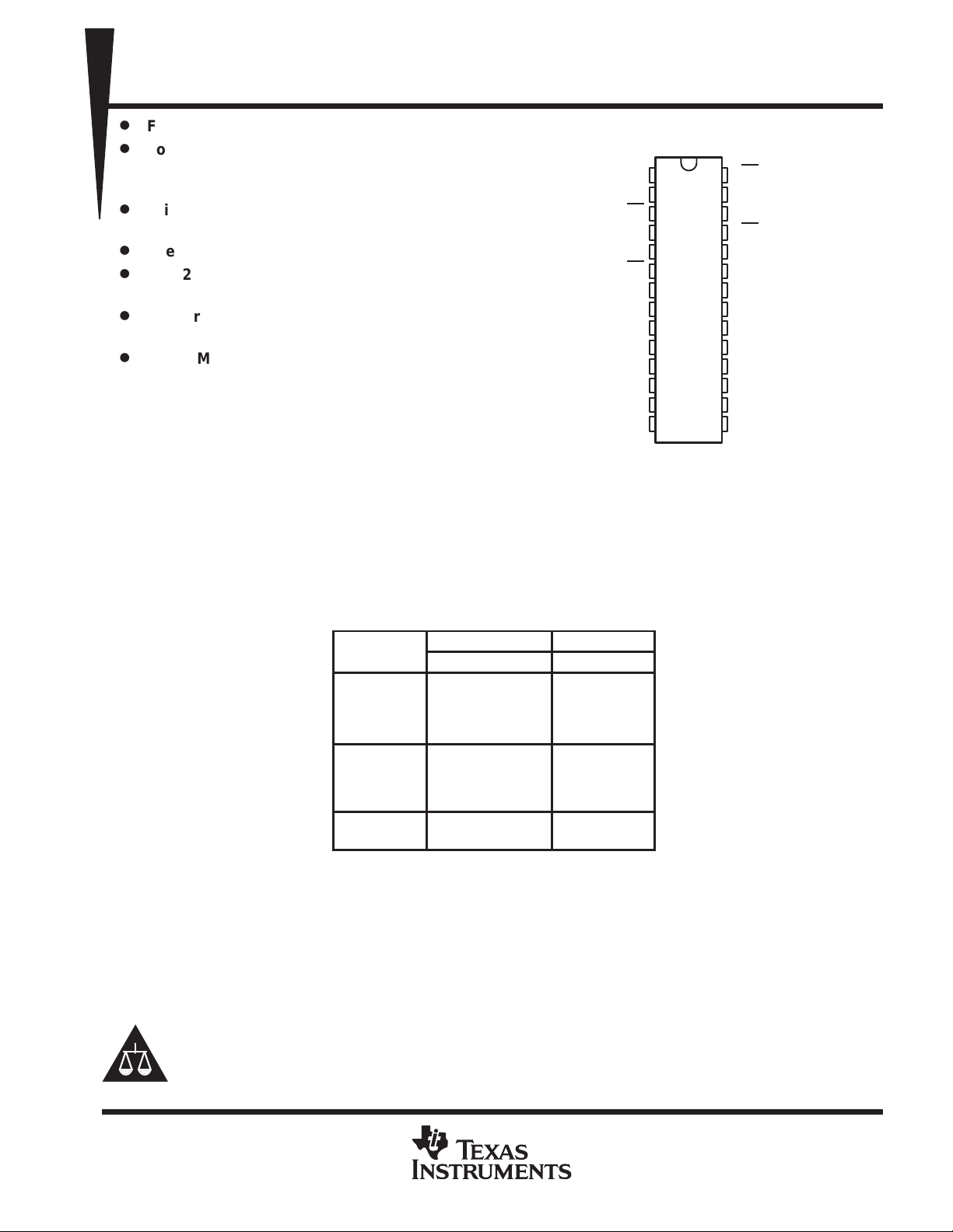
DW PACKAGE
3A
3Z
3LB
4A
4Z
4LB
V
SS
GND
4B
4Y
3B
3Y
3C
4C
(TOP VIEW)
1
28
2
27
3
26
4
25
5
24
6
23
7
22
8
21
9
20
10
19
11
18
12
17
13
16
14
15
2LB
2Z
2A
1LB
1Z
1A
R
WS
V
DD
1Y
1B
2Y
2B
2C
1C
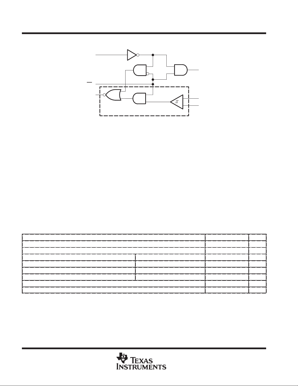
RS-423-B driver and receiver with integratedloopback function. The operation of the
SN75LBC786 is closely based on that of the SN75186. In normal operation, the device performs as four
independent RS-423-B driver/receiver pairs designed to interface data-terminal equipment (DTE) with data
circuit-terminating equipment (DCE). In loopback mode, the signal from each driver output is fed back via
special circuitry into its associated receiver input, removing the need to locally disconnect cables and install a
loopback connector. The receiver output signal is the same as the driver input signal.
The SN75LBC786 is characterized for operation over the temperature range of 0°C to 70°C.
FUNCTION TABLE
LOOPBACK
LB
H L HL L H
H H HL L L
H
H
H
H
L
L
H = high level, L = low level, X = irrelevant, ? = indeterminate
INPUTS OUTPUTS
A B C Z Y
L
L
L
H
L
H
L
H
L
H
H
X
X
L
H
H
X
X
?
?
?
?
L
H
L
H
L
H
L
L
L
Please be aware that an important notice concerning availability, standard warranty, and use in critical applications of
Texas Instruments semiconductor products and disclaimers thereto appears at the end of this data sheet.
LinBiCMOS is a trademark of Texas Instruments Incorporated.
PRODUCTION DATA information is current as of publication date.
Products conform to specifications per the terms of Texas Instruments
standard warranty. Production processing does not necessarily include
testing of all parameters.
POST OFFICE BOX 655303 • DALLAS, TEXAS 75265
Copyright 1994, T exas Instruments Incorporated
1
SN75LBC786
QUADRUPLE RS-423-B DRIVER/RECEIVER WITH LOOPBACK
SLLS184 – NOVEMBER 1994
logic diagram (positive logic) (each transceiver)
Driver
A
LB
Y
Z
Receiver
–
+
C
B
absolute maximum ratings over operating free-air temperature range (unless otherwise noted)
Positive supply voltage, V
Negative supply voltage, V
Receiver input voltage range –30 V to 30 V. . . . . . . . . . . . . . . . . . . . . . . . . . . . . . . . . . . . . . . . . . . . . . . . . . . . . . . .
Driver input voltage range –0.5 V to 5.75 V. . . . . . . . . . . . . . . . . . . . . . . . . . . . . . . . . . . . . . . . . . . . . . . . . . . . . . . .
Loopback input voltage range –0.5 V to 5.75 V. . . . . . . . . . . . . . . . . . . . . . . . . . . . . . . . . . . . . . . . . . . . . . . . . . . .
Driver output voltage range (supplies at 0 V) –30 V to 30 V. . . . . . . . . . . . . . . . . . . . . . . . . . . . . . . . . . . . . . . . . .
Driver output voltage range (supplies at ±12 V) –25 V to 25 V. . . . . . . . . . . . . . . . . . . . . . . . . . . . . . . . . . . . . . . .
Continuous power dissipation at (or below) T
Operating free-air temperature range, T
Storage temperature range, T
Case temperature for 10 seconds 260°C. . . . . . . . . . . . . . . . . . . . . . . . . . . . . . . . . . . . . . . . . . . . . . . . . . . . . . . . . .
†
Stresses beyond those listed under “absolute maximum ratings” may cause permanent damage to the device. These are stress ratings only, and
functional operation of the device at these or any other conditions beyond those indicated under “recommended operating conditions” is not
implied. Exposure to absolute-maximum-rated conditions for extended periods may affect device reliability.
NOTE 1: All voltages are with respect to network ground terminal.
(see Note 1) 14 V. . . . . . . . . . . . . . . . . . . . . . . . . . . . . . . . . . . . . . . . . . . . . . . . . . . . .
DD
–14 V. . . . . . . . . . . . . . . . . . . . . . . . . . . . . . . . . . . . . . . . . . . . . . . . . . . . . . . . . . . . . . .
SS
= 70°C 800 mW. . . . . . . . . . . . . . . . . . . . . . . . . . . . . . . . . . . . . . . .
A
0°C to 70°C. . . . . . . . . . . . . . . . . . . . . . . . . . . . . . . . . . . . . . . . . . . . . .
–65°C to 150°C. . . . . . . . . . . . . . . . . . . . . . . . . . . . . . . . . . . . . . . . . . . . . . . . . . .
stg
A
recommended operating conditions
MIN NOM MAX UNIT
Supply voltage, V
Supply voltage, V
High-level input voltage, V
Low-level input voltage, V
High-level output current, I
Low-level output current, I
Slew rate control resistor, R
Operating free-air temperature, T
DD
SS
IH
IL
OH
OL
WS
Driver and loopback 2 V
Driver and loopback 0.8 V
Receiver –4 mA
Receiver 4 mA
A
10.8 12 13.2 V
–10.8 –12 –13.2 V
20 82 820 kΩ
0 70 °C
†
2
POST OFFICE BOX 655303 • DALLAS, TEXAS 75265
IDDSupply current (loopback off)
mA
ISSSupply current (loopback off)
mA
s
(see Figure 1)
L
s
(see Figure 1)
SN75LBC786
QUADRUPLE RS-423-B DRIVER/RECEIVER WITH LOOPBACK
SLLS184 – NOVEMBER 1994
DRIVER SECTION
electrical characteristics over recommended ranges of supply voltage and operating free-air
temperature (unless otherwise noted)
PARAMETER TEST CONDITIONS MIN TYP MAX UNIT
V
OH
V
OL
I
IH
I
IL
I
IKG
I
OS(H)
I
OS(L)
I
DD(LB)
I
DD
LOOPBACK MODE
High-level output voltage Open circuit or RI = 450 Ω 4 5.5 6 V
Low-level output voltage Open circuit or RI = 450 Ω –6 –5.5 –4 V
High-level input current VI = 2.4 V – 5.5 V 100 µA
Low-level input current VI = 0 V – 0.8 V –100 µA
Output leakage current VDD = VSS = 0 V, VO = ±6 V –100 100 µA
High-level short-circuit output current VI = high, VO = 0 V 15 45 mA
Low-level short-circuit output current VI = low, VO = 0 V –45 –15 mA
pp
Supply current with loopback on No load, LB at 0.8 V 13 16 mA
pp
Supply current with loopback on No load, LB at 0.8 V –13 –16 mA
Output voltage (input either high or low) RI = >450 Ω, VLB = low –6 –5.5 –4 V
p
p
No load, LB at 2 V 10 12
RI = 450 Ω, LB at 2 V 60 70
No load, LB at 2 V –10 –12
RI = 450 Ω, LB at 2 V –60 –70
switching characteristics over recommended ranges of supply voltage and operating free-air
temperature (unless otherwise noted)
PARAMETER TEST CONDITIONS MIN TYP MAX UNIT
RWS = 0 kΩ 1.5
Transition time, low-to-high level output
t
TLH
RI = 450 Ω, CL = 50 pF,
VWS = 5 V
Transition time, high-to-low level output
t
THL
SR Output slew rate RWS = 20 kΩ 15 V/µs
t
sk
Output skew, |t
PHL
– t
| (see Figure 4) RWS = 82 kΩ 1 µs
PLH
RWS = 20 kΩ 1.5 2.1 2.7
RWS = 82 kΩ 5 8 11
RWS = 820 kΩ 80
RWS = 0 kΩ
RWS = 20 kΩ 1.5 2.1 2.7
RWS = 82 kΩ 5 8 11
RWS = 820 kΩ 80
1.5
µ
µ
POST OFFICE BOX 655303 • DALLAS, TEXAS 75265
3
 Loading...