

SN75LBC784
QUADRUPLE RS-423-B DRIVER/RECEIVER
SLLS187A – NOVEMBER 1994 – REVISED AUGUST 1995
1
POST OFFICE BOX 655303 • DALLAS, TEXAS 75265
D
Four Independent Drivers and Receivers
D
Driver Slew Rate Controlled by a Single
Resistor
D
Fast Driver Transition Times Down to
1.5 µs and Receiver Transition Times of
20 ns Typ
D
Internal Thermal-Overload Protection
D
RS-423-B Inputs and Outputs Designed to
Withstand ±25 V
D
ESD Protection Exceeds 2000 V Per
MIL-STD-833C Method 3015
D
LinBICMOS Process Technology
description
The SN75LBC784 performs as four independent
RS-423-B driver/receiver pairs designed to
interface data terminal equipment (DTE) with data
circuit-terminating equipment (DCE) at rates up to
120 kbps and distances to 1.2 km. The
SN75LBC784 provides an upgrade to the RS-232
serial interface and can be backward compatible
with existing serial ports while offering the higher
performance required by new faster peripherals,
such as v.34 (v.fast) modems. The RS-232
standard, and subsequent revisions, only support
data rates up to 20 kbps over about 15 meters of
cable. For RS-423-B the data rate is increased to
120 kbps and transmission distance to 1.2 km by
reducing the maximum output signal swing,
increasing the driver output current, and reducing
the receiver input voltage thresholds.
The receivers consist of differential comparators with hysteresis and resistive attenuation on the inputs. The
resistive attenuation improves the input common mode range and also provides additional protection from ESD
and over-voltage stress. The differential and common mode input impedances are sufficiently high to meet
RS-423-B. When a differential voltage input of 500 mV is applied across the entire common mode range ( see
Figure 5), the receiver characteristics and bias voltage allow the receiver to remain in its intended binary state.
The drivers meet all RS-423-B specifications with built-in current limits and thermal-overload protection.
Slew-rate controlling circuitry is included in the design, which is adjusted to suit the application by means of an
external resistor (R
ws)
. The slew rate controlling circuitry also has a default mode – if the Rws pin is shorted to
5 V externally, the transistion time defaults to approximately 1.5 ms. The BIAS input, when shorted to 5 V
externally, provides the internal node voltages. The receiver is compatible to RS-232 with the use of external
input resistors to meet the RS-232 input resistance specification of 3 kΩ to 7 kΩ.
The SN75LBC784 is characterized for operation over the temperature range of 0°C to 70°C.
LinBiCMOS is a trademark of Texas Instruments Incorporated.
Copyright 1995, Texas Instruments Incorporated
PRODUCTION DATA information is current as of publication date.
Products conform to specifications per the terms of Texas Instruments
standard warranty. Production processing does not necessarily include
testing of all parameters.
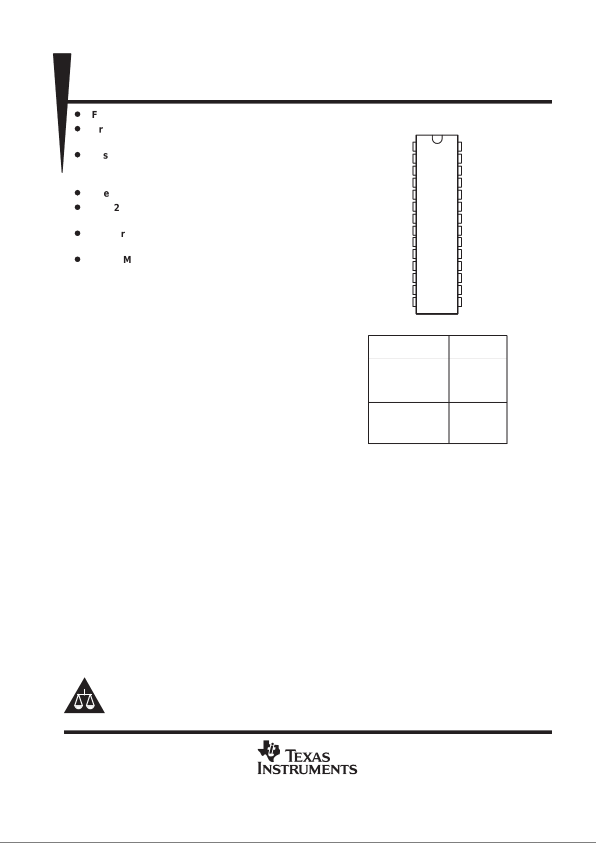
1
2
3
4
5
6
7
8
9
10
11
12
13
14
28
27
26
25
24
23
22
21
20
19
18
17
16
15
3A
3Z
BIAS
4A
4Z
BIAS
V
SS
GND
4B
4Y
3B
3Y
3C
4C
BIAS
2Z
2A
BIAS
1Z
1A
R
ws
V
DD
1Y
1B
2Y
2B
2C
1C
DW PACKAGE
(TOP VIEW)
INPUTS OUTPUTS
L
H
L
H
FUNCTION TABLE
AB
L
L
H
H
H
H
L
L
H
H
L
L
ZY
H
L
H
L
H = high level, L = low level,
X = irrelevant, Z = high impedance (off)
? = indeterminate
L
H
L
H
L
L
H
H
L
L
H
H
?
?
?
?
H
L
H
L
C
Please be aware that an important notice concerning availability, standard warranty, and use in critical applications of
Texas Instruments semiconductor products and disclaimers thereto appears at the end of this data sheet.
SN75LBC784
QUADRUPLE RS-423-B DRIVER/RECEIVER
SLLS187A – NOVEMBER 1994 – REVISED AUGUST 1995
2
POST OFFICE BOX 655303 • DALLAS, TEXAS 75265
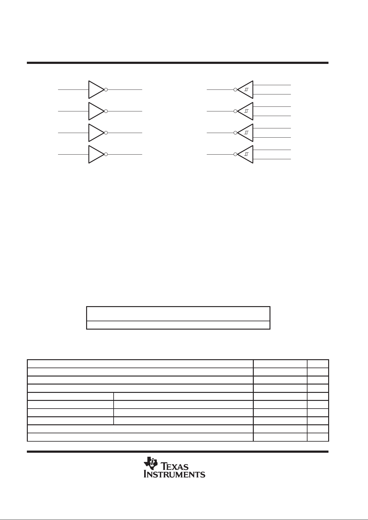
logic diagram (positive logic)
_
+
121
2
11
13
3Y
3B
3C
3A
3Z
104
4Y
4A
2023
1Y
1A
1826
2Y
2A
_
+
5
9
14
4B
4C
4Z
_
+
27
19
15
1B
1C
1Z
_
+
24
17
16
2B
2C
2Z
absolute maximum ratings over operating free-air temperature range (unless otherwise noted)
†
Positive supply voltage, V
DD
(see Note 1) 14 V. . . . . . . . . . . . . . . . . . . . . . . . . . . . . . . . . . . . . . . . . . . . . . . . . . . . .
Negative supply voltage, V
SS
–14 V. . . . . . . . . . . . . . . . . . . . . . . . . . . . . . . . . . . . . . . . . . . . . . . . . . . . . . . . . . . . . . .
Bias voltage, V
bias
5.75 V. . . . . . . . . . . . . . . . . . . . . . . . . . . . . . . . . . . . . . . . . . . . . . . . . . . . . . . . . . . . . . . . . . . . . . .
Receiver input voltage range –30 V to 30 V. . . . . . . . . . . . . . . . . . . . . . . . . . . . . . . . . . . . . . . . . . . . . . . . . . . . . . . .
Driver input voltage range –0.5 V to 5.75 V. . . . . . . . . . . . . . . . . . . . . . . . . . . . . . . . . . . . . . . . . . . . . . . . . . . . . . . .
Driver output voltage range (supplies at 0 V) –30 V to 30 V. . . . . . . . . . . . . . . . . . . . . . . . . . . . . . . . . . . . . . . . . .
Driver output voltage range (supplies at ±12 V) –25 V to 25 V. . . . . . . . . . . . . . . . . . . . . . . . . . . . . . . . . . . . . . . .
Continuous power dissipation See Dissipation Rating Table. . . . . . . . . . . . . . . . . . . . . . . . . . . . . . . . . . . . . . . . .
Operating free-air temperature range, T
A
0°C to 70°C. . . . . . . . . . . . . . . . . . . . . . . . . . . . . . . . . . . . . . . . . . . . . .
Storage temperature range –65°C to 150°C. . . . . . . . . . . . . . . . . . . . . . . . . . . . . . . . . . . . . . . . . . . . . . . . . . . . . . . .
Case temperature for 10 seconds 260°C. . . . . . . . . . . . . . . . . . . . . . . . . . . . . . . . . . . . . . . . . . . . . . . . . . . . . . . . . .
†
Stresses beyond those listed under “absolute maximum ratings” may cause permanent damage to the device. These are stress ratings only, and
functional operation of the device at these or any other conditions beyond those indicated under “recommended operating conditions” is not
implied. Exposure to absolute-maximum-rated conditions for extended periods may affect device reliability.
NOTE 1: All voltages are with respect to network ground terminal.
DISSIPATION RATING TABLE
PACKAGE
TA ≤ 25°C
POWER RATING
DERATING FACTOR
†
ABOVE TA = 25°C
TA = 70°C
POWER RATING
DW 1348 mW 10.8 mW/°C 862 mW
†
Derating factors are the inverse of the junction-to-ambient thermal resistance when
board-mounted with no air flow .
recommended operating conditions
MIN NOM MAX UNIT
Supply voltage, V
DD
10.8 12 13.2 V
Supply voltage, V
SS
–10.8 –12 –13.2 V
Bias voltage, V
bias
2 5 5.5 V
High-level input voltage, V
IH
Driver 2 V
Low-level input voltage, V
IL
Driver 0.8 V
High-level output current, I
OH
Receiver –4 mA
Low-level output current, I
OL
Receiver 4 mA
Rws slew rate control resistor 20 82 820 kΩ
Operating free-air temperature, T
A
0 70 °C
SN75LBC784
QUADRUPLE RS-423-B DRIVER/RECEIVER
SLLS187A – NOVEMBER 1994 – REVISED AUGUST 1995
3
POST OFFICE BOX 655303 • DALLAS, TEXAS 75265
DRIVER SECTION
electrical characteristics over recommended ranges of supply voltage and operating free-air
temperature, V
DD
= 10.8 V to 13.2 V, VSS = –10.8 V to –13.2 V, TA = 0°C to 70°C (unless otherwise
noted)
PARAMETER TEST CONDITIONS MIN TYP MAX UNIT
V
OH
High-level output voltage Open circuit or RL = 450 Ω 4 5.5 6 V
V
OL
Low-level output voltage Open circuit or RL = 450 Ω –6 –5.5 –4 V
I
IH
High-level input current VI = 2.4 V to 5.5 V 100 µA
I
IL
Low-level input current VI = 0 V to 0.8 V –100 µA
I
O
Output leakage current VDD = VSS = 0, VO = ±6 V –100 100 µA
I
OS(H)
High-level short circuit output current VI = 5 V, VO = 0 15 45 mA
I
OS(L)
Low-level short circuit output current VI = 0, VO = 0 –45 –15 mA
pp
No load 10 12
IDDSupply current
RL = 450 Ω 60 70
mA
pp
No load –10 –12
ISSSupply current
RL = 450 Ω –60 –70
mA
I
bias
Bias current 400 µA
switching characteristics over recommended ranges of supply voltage and operating free-air
temperature, V
DD
= 10.8 V to 13.2 V, VSS = –10.8 V to –13.2 V, TA = 0°C to 70°C (unless otherwise
noted)
PARAMETER TEST CONDITIONS MIN TYP MAX UNIT
Rws = 0 kΩ 1.5
Rws = 20 kΩ 1.5 2.1 2.7
t
TLH
Transition time, low-to-high level (see Figure 1)
Rws = 82 kΩ 5 8 11
µ
s
Rws = 820 kΩ 80
RL = 450 Ω, CL = 50 pF,
Rws = 0 kΩ
1.5
L
VWS = 5 V
L
Rws = 20 kΩ 1.5 2.1 2.7
t
THL
Transition time, high-to-low level (see Figure 1)
Rws = 82 kΩ 5 8 11
µ
s
Rws = 820 kΩ 80
SR Output slew rate Rws = 20 kΩ 15 V/µs
t
sk
Output skew (see Figure 4) |t
PHL
– t
PLH
| Rws = 82 kΩ 1 µs

SN75LBC784
QUADRUPLE RS-423-B DRIVER/RECEIVER
SLLS187A – NOVEMBER 1994 – REVISED AUGUST 1995
4
POST OFFICE BOX 655303 • DALLAS, TEXAS 75265
RECEIVER SECTION
electrical characteristics over recommended ranges of supply voltage and operating free-air
temperature, V
DD
= 10.8 V to 13.2 V, VSS = –10.8 V to –13.2 V, TA = 0°C to 70°C (unless otherwise
noted)
PARAMETER TEST CONDITIONS MIN TYP MAX UNIT
p
200
V
IT+
Positive input threshold voltage
With 500 Ω series resistor 400
mV
p
–200
V
IT–
Negative input threshold voltage
With 500 Ω series resistor –400
mV
p
VI = 10 V
p
1.3 3.25
IIInput current
VI = –10 V
Other input to GND
–3.25 –1.3
mA
V
hys
Hysteresis (V
IT+
– V
IT–
) 20 40 150 mV
p
IO = –20 µA 3.5 5
VOHHigh-level output voltage (see Note 2)
IO = –4 mA 2.4 5
V
V
OL
Low-level output voltage IO = 20 µA to 4 mA 0.4 V
I
RX
RX short circuit current 50 mA
V
ID
Differential input voltage Receiver inputs open circuit 1.6 2.1 2.6 V
V
ofs
Fail safe output voltage See Note 3 3.5 V
NOTES: 2. Device has an internal RX supply regulator . Maximum RX logic output voltage under no load is thus defined by an internal voltage
value. This is nominally set to 4.5 V with a tolerance of ±5%.
3. One input at ground, other input open circuit, IO = –20 µA, or both open circuit.
switching characteristics over recommended ranges of supply voltage and operating free-air
temperature (unless otherwise noted)
test conditions: VDD = 10.8 V to 13.2 V, VSS = –10.8 V to –13.2 V , TA = 0°C to 70°C (unless otherwise noted)
PARAMETER TEST CONDITIONS MIN NOM MAX UNIT
t
PLH
Propagation Delay time low-to-high (see Figure 2)
t
PHL
Propagation delay time high-to-low (see Figure 2)
p
0.15
1µs
t
THL
Transition time high-to-low (see Figure 3)
C
L
= 50
pF
t
TLH
Transition time low-to-high (see Figure 3)
20
200
ns

SN75LBC784
QUADRUPLE RS-423-B DRIVER/RECEIVER
SLLS187A – NOVEMBER 1994 – REVISED AUGUST 1995
5
POST OFFICE BOX 655303 • DALLAS, TEXAS 75265
PARAMETER MEASUREMENT INFORMATION
V
DD
V
SS
R
L
C
L
51 Ω
Input
R
ws
Output
5 V
t
THL
t
TLH
90% 90%
10% 10%
V
OH
V
OL
Output
Input
(see Note A and B)
GND
GND
3 V
0 V
Figure 1. Driver Transition T imes
V
DD
V
SS
C
L
Input
Output
t
PHL
t
PLH
Output
Input
(see Note A and C)
GND
GND
50% 50%
50% 50%
51 Ω
0.5 V
– 0.5 V
+
–
Figure 2. Receiver Propagation Delay Times
t
THL
t
TLH
90% 90%
10% 10%
V
OH
V
OL
Output
Input
(see Note A and C)
V
DD
V
SS
C
L
Input
Output
GND
GND
+
–
0.5 V
–0.5 V
51 Ω
Figure 3. Receiver Transition Times
NOTES: A. CL includes probe and jig capacitance.
B. The input pulse is supplied by a generator having the following characteristics: tr ≤ 10 nS, tf < 10 nS, Zo = 50 Ω, PRR ≥ 5 kHz, duty
cycle 50%, V
max
= 3 V, V
min
= 0 V.
C. The input pulse is supplied by a generator having the following characteristics: tr ≤ 10 nS, tf < 10 nS, Zo = 50 Ω, PRR ≥ 5 kHz, duty
cycle 50%, V
max
= 0.5 V, V
min
= –0.5 V.

SN75LBC784
QUADRUPLE RS-423-B DRIVER/RECEIVER
SLLS187A – NOVEMBER 1994 – REVISED AUGUST 1995
6
POST OFFICE BOX 655303 • DALLAS, TEXAS 75265
PARAMETER MEASUREMENT INFORMATION
50% 50%
50% 50%
t
PLH
t
PHL
Input A
Output Y
Figure 4. Skew Definition Times
V
cm
250 mW
250 mW
500 Ω
500 Ω
Vcm = –7 to 7 V
Figure 5. Receiver Input Balance Test

IMPORTANT NOTICE
T exas Instruments and its subsidiaries (TI) reserve the right to make changes to their products or to discontinue
any product or service without notice, and advise customers to obtain the latest version of relevant information
to verify, before placing orders, that information being relied on is current and complete. All products are sold
subject to the terms and conditions of sale supplied at the time of order acknowledgement, including those
pertaining to warranty, patent infringement, and limitation of liability.
TI warrants performance of its semiconductor products to the specifications applicable at the time of sale in
accordance with TI’s standard warranty. Testing and other quality control techniques are utilized to the extent
TI deems necessary to support this warranty. Specific testing of all parameters of each device is not necessarily
performed, except those mandated by government requirements.
CERT AIN APPLICATIONS USING SEMICONDUCTOR PRODUCTS MAY INVOLVE POTENTIAL RISKS OF
DEATH, PERSONAL INJURY, OR SEVERE PROPERTY OR ENVIRONMENTAL DAMAGE (“CRITICAL
APPLICATIONS”). TI SEMICONDUCTOR PRODUCTS ARE NOT DESIGNED, AUTHORIZED, OR
WARRANTED TO BE SUITABLE FOR USE IN LIFE-SUPPORT DEVICES OR SYSTEMS OR OTHER
CRITICAL APPLICATIONS. INCLUSION OF TI PRODUCTS IN SUCH APPLICA TIONS IS UNDERST OOD TO
BE FULLY AT THE CUSTOMER’S RISK.
In order to minimize risks associated with the customer’s applications, adequate design and operating
safeguards must be provided by the customer to minimize inherent or procedural hazards.
TI assumes no liability for applications assistance or customer product design. TI does not warrant or represent
that any license, either express or implied, is granted under any patent right, copyright, mask work right, or other
intellectual property right of TI covering or relating to any combination, machine, or process in which such
semiconductor products or services might be or are used. TI’s publication of information regarding any third
party’s products or services does not constitute TI’s approval, warranty or endorsement thereof.
Copyright 1998, Texas Instruments Incorporated
 Loading...