

SN75LBC775
SINGLE-CHIP APPLETALK AND LOCALTALK TRANSCEIVER
SLLS216A – MA Y 1995 – REVISED JANUARY 1996
1
POST OFFICE BOX 655303 • DALLAS, TEXAS 75265
POST OFFICE BOX 1443
• HOUSTON, TEXAS 77251–1443
D
Single-Chip Interface Solution for
AppleTalk and LocalTalk
D
Designed to Operate Up To 1 Mbps In
AppleTalk and LocalTalk
D
Switched-Capacitor Voltage Converter
Allows for Single 5-V Operation
D
4-kV ESD Protection on Bus Terminals
D
Combines Multiple Components into a
Single Chip Solution
D
LinBiCMOS Process Technology
description
The SN75LBC775 is a low-power LinBiCMOS
device that incorporates the drivers and receivers
for an AppleTalk or a LocalTalk interface and a
switched-capacitor voltage converter for a single
5-V supply operation. LocalTalk uses a hybrid of
RS-422 with the transceiver connected to the
network through a small isolation transformer.
The AppleTalk mode provides point-to-point
communications and uses the same differential
driver and receiver as LocalTalk with the addition
of a hybrid RS-423, single-ended handshake
driver (HSK) and receiver. In the AppleTalk mode,
the port connects directly to the receiver with no
isolation transformer.
While the device power is turned off (V
CC
= 0) or
disabled in the LocalT alk mode, the outputs are in
a high-impedance state. When the driver enable
(DEN
) terminal is high, both the differential and
serial driver outputs are in a high-impedance
state.
The receiver output can be disabled and becomes
a high impedance when the REN terminal is low.
A switched-capacitor voltage converter generates
the negative voltage required from a single 5-V
supply using two 22-µF capacitors. One capacitor
is between the C+ and C– terminals and the
second is between V
SS
and ground.
The SN75LBC775 is characterized for operating
over the temperature range of 0°C to 70°C.
Please be aware that an important notice concerning availability, standard warranty, and use in critical applications of
Texas Instruments semiconductor products and disclaimers thereto appears at the end of this data sheet.
1
2
3
4
5
6
7
8
9
10
20
19
18
17
16
15
14
13
12
11
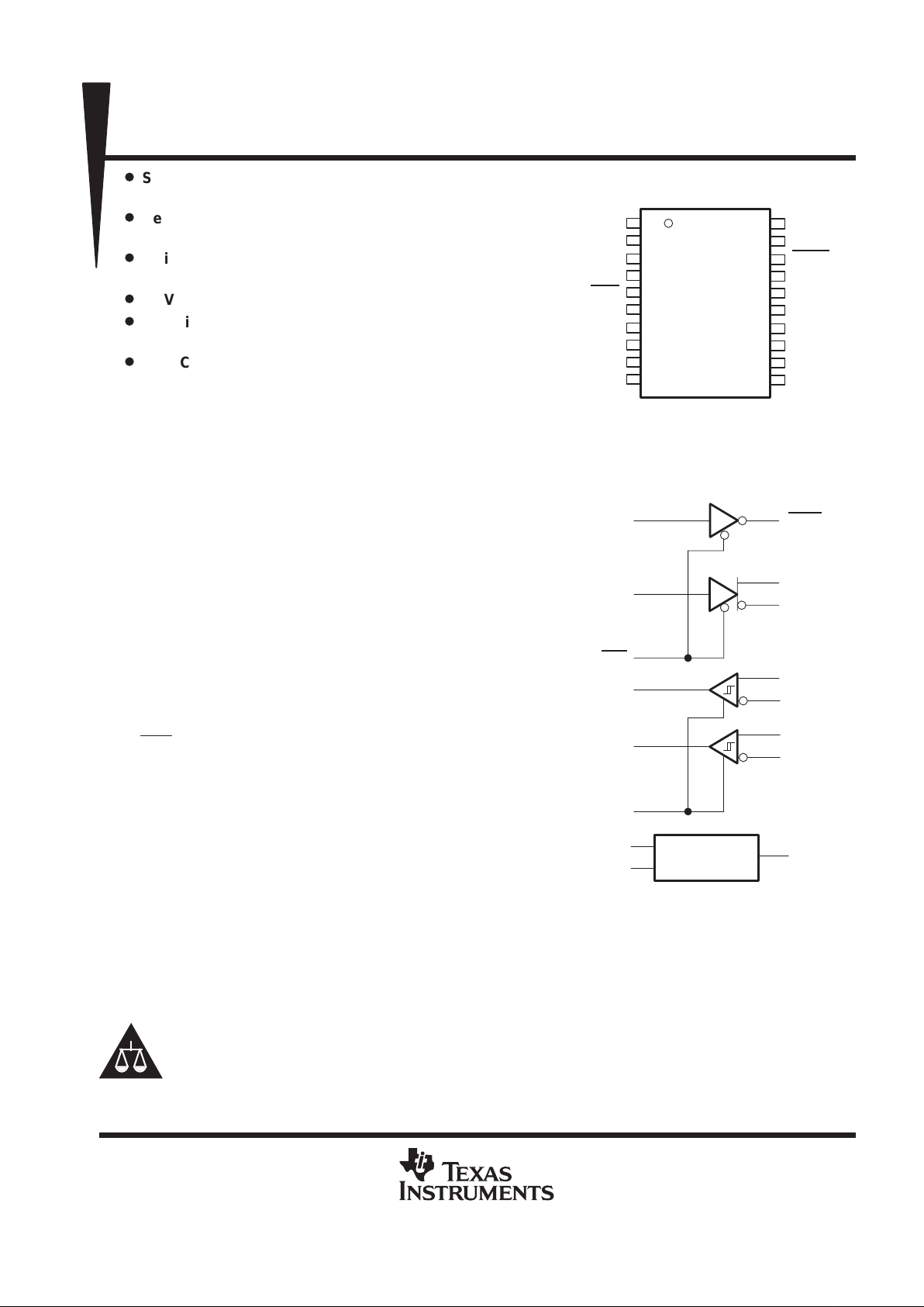
HSKA
V
SS
C–
C+
DEN
DY
DZ
GND
V
CC
DA
GND
V
CC
HSKY
RY2
RA2
RB2
RB1
RA1
RY1
REN
DW PACKAGE
(TOP VIEW)
functional diagram
HSKY
DY
DZ
RY1
RY2
HSKA
DA
DEN
RA1
RB1
REN
RA2
RB2
Charge Pump
V
SS
–5 V
V
CC
GND
1
10
5
12
17
11
19
8
18
6
7
13
14
16
15
2
PRODUCTION DATA information is current as of publication date.
Products conform to specifications per the terms of Texas Instruments
standard warranty. Production processing does not necessarily include
testing of all parameters.
Copyright 1996, Texas Instruments Incorporated
LocalTalk and AppleTalk are trademarks of Apple Computer, Inc.
LinBiCMOS is a trademark of Texas Instruments Incorporated.
SN75LBC775
SINGLE-CHIP APPLETALK AND LOCALTALK TRANSCEIVER
SLLS216A – MA Y 1995 – REVISED JANUARY 1996
2
POST OFFICE BOX 655303 • DALLAS, TEXAS 75265
POST OFFICE BOX 1443
• HOUSTON, TEXAS 77251–1443
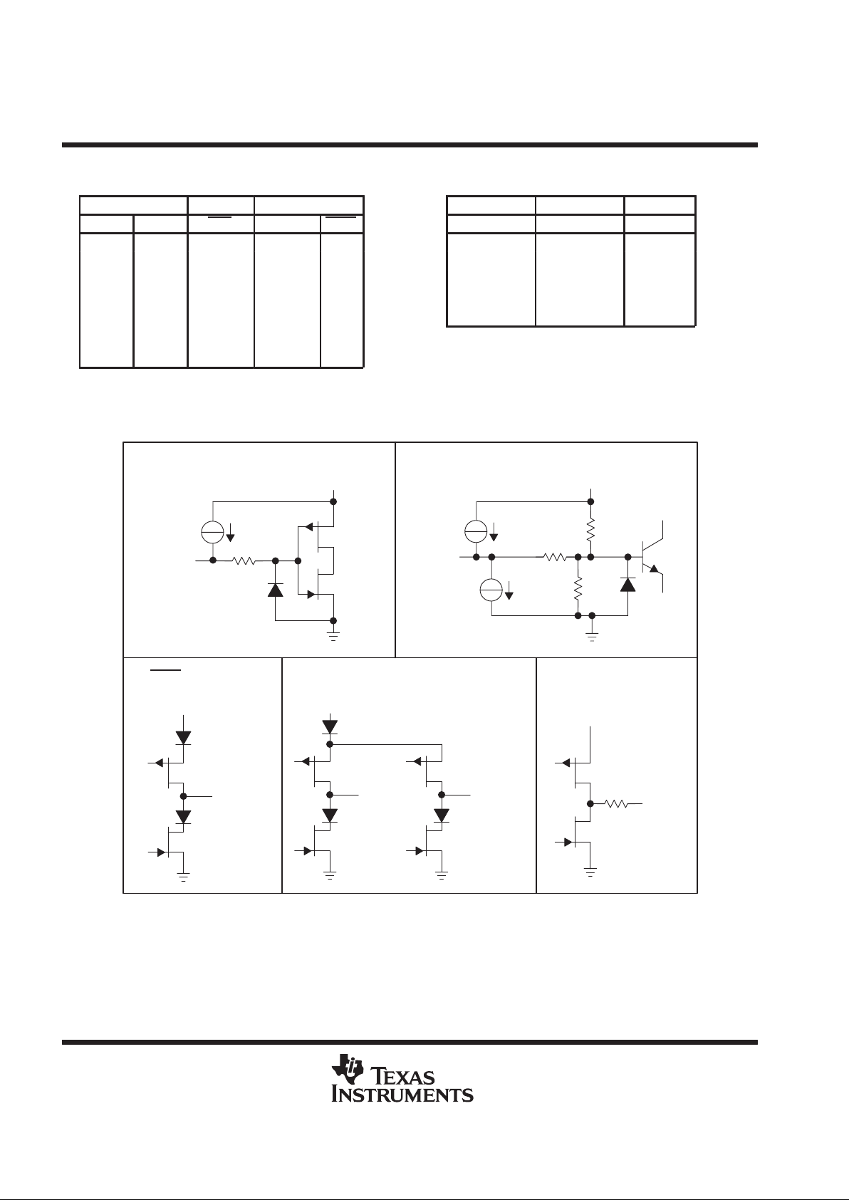
DRIVER FUNCTION TABLE RECEIVER FUNCTION TABLE
INPUT
ENABLE OUTPUT INPUT ENABLE OUTPUT
DA HSKA DEN ABHSKY RA RB REN RY
H X L HL X HL H H
L X L LHX LH H L
X H L XX L OPEN H H
X L L XX H SHORT
†
H ?
OPEN OPEN L HL L X L Z
X X H ZZ
Z
†
–0.2 V < VID < 0.2 V
X X OPEN ZZ Z
H = high level, L = low level, X = irrelevant, ? = indeterminate, Z = high impedance (off)
schematics of inputs and outputs
Input
V
CC
1 kΩ
10 kΩ
B Input
Only
A Input
Only
24 kΩ
5 kΩ
V
CC
Input
V
CC
Output
V
CC
DY
Output
DZ
Output
V
CC
4 kΩ
Output
ALL LOGIC INPUTS RECEIVER INPUTS
HSKY
OUTPUT DY AND DZ OUTPUTS RECEIVER OUTPUTS
SN75LBC775
SINGLE-CHIP APPLETALK AND LOCALTALK TRANSCEIVER
SLLS216A – MA Y 1995 – REVISED JANUARY 1996
3
POST OFFICE BOX 655303 • DALLAS, TEXAS 75265
POST OFFICE BOX 1443
• HOUSTON, TEXAS 77251–1443
absolute maximum ratings over operating free-air temperature range (unless otherwise noted)
†
Supply voltage range, V
CC
(see Note 1) –0.5 to 7 V. . . . . . . . . . . . . . . . . . . . . . . . . . . . . . . . . . . . . . . . . . . . . . . .
Supply voltage range, V
SS
–7 to 0.5 V. . . . . . . . . . . . . . . . . . . . . . . . . . . . . . . . . . . . . . . . . . . . . . . . . . . . . . . . . . . .
Receiver input voltage range, V
I
(RA) –15 V to 15 V. . . . . . . . . . . . . . . . . . . . . . . . . . . . . . . . . . . . . . . . . . . . . . . .
Receiver differential input voltage range, V
ID
–12 V to 12 V. . . . . . . . . . . . . . . . . . . . . . . . . . . . . . . . . . . . . . . . .
Receiver output voltage range, V
O
(RY) –0.5 V to 5.5 V. . . . . . . . . . . . . . . . . . . . . . . . . . . . . . . . . . . . . . . . . . . .
Driver output voltage range, V
O
(Power Off) (DY, DZ, HSKY) –15 V to 15 V. . . . . . . . . . . . . . . . . . . . . . . . .
(Power On) (DY, DZ, HSKY
) –11 V to 11 V. . . . . . . . . . . . . . . . . . . . . . . .
Driver input voltage range, V
I
(DA, HSKA, DEN, REN) –0.5 V to V
CC
+ 0.4 V. . . . . . . . . . . . . . . . . . . . . . . . . .
Electrostatic discharge
(see Note 2) Class 3, A: Bus terminals 4 kV. . . . . . . . . . . . . . . . . . . . . . . . . . . . . .
All other terminals 2 kV. . . . . . . . . . . . . . . . . . . . . . . . . .
Continuous total power dissipation See Dissipation Rating Table. . . . . . . . . . . . . . . . . . . . . . . . . . . . . . . . . . . . .
Operating free-air temperature range,T
A
0°C to 70°C. . . . . . . . . . . . . . . . . . . . . . . . . . . . . . . . . . . . . . . . . . . . . .
†
Stresses beyond those listed under “absolute maximum ratings” may cause permanent damage to the device. These are stress ratings only, and
functional operation of the device at these or any other conditions beyond those indicated under “recommended operating conditions” is not
implied. Exposure to absolute-maximum-rated conditions for extended periods may affect device reliability.
NOTES: 1. All voltage values are with respect to network ground terminal unless otherwise noted.
2. This maximum rating is tested according to MIL-STD-883C, Method 3015.7.
DISSIPATION RATING TABLE
T
≤ 25°C DERATING FACTOR T
= 85°C
PACKAGE
A
POWER RATING ABOVE TA = 25°CAPOWER RATING
DW 1125 mW 9.0 mW/°C 585 mW
recommended operating conditions
MIN NOM MAX UNIT
Supply voltage, V
CC
4.75 5 5.25 V
High-level input voltage, V
IH
DA, HSKA, DEN, REN 2 V
Low-level input voltage, V
IL
DA, HSKA, DEN, REN 0.8 V
Receiver input common-mode voltage range, V
ICR
‡
–7 7 V
Differential input voltage, V
ID
‡
–12 12 V
Voltage-converter filter capacitance 22 µF
Voltage-converter filter-capacitor equivalent series resistance (ESR) 2 Ω
Operating free-air temperature, T
A
0 70
°C
‡
The algebraic convention, in which the less-positive (more negative) limit is designated minimum, is used in this data sheet.
SN75LBC775
SINGLE-CHIP APPLETALK AND LOCALTALK TRANSCEIVER
SLLS216A – MA Y 1995 – REVISED JANUARY 1996
4
POST OFFICE BOX 655303 • DALLAS, TEXAS 75265
POST OFFICE BOX 1443
• HOUSTON, TEXAS 77251–1443
DRIVER
electrical characteristics over recommend operating characteristics (unless otherwise noted)
PARAMETER TEST CONDITIONS MIN TYP†MAX UNIT
V
OH
High-level output voltage
3.7 V
V
OL
Low-level output voltage
Single ended
R
L
= 3 kΩ,
See Figure 1
–3.7 V
|VOD| Magnitude of differential output voltage (VDY – VDZ) See Figure 2 4.0 5.6 V
∆|VOD| Change in differential voltage magnitude See Figure 2 10 250 mV
V
OC
Common-mode output voltage
‡
See Figure 3 –1 3 V
∆V
OC(SS)
Change in steady-state common-mode output voltage See Figure 3 ±200 mV
I
OZ
High-impedance output current VCC = 0, –10 V ≤ VO ≤ 10 V ±100 µA
I
OS
Short-circuit output current –5 V ≤VO ≤5 V 450 mA
I
CC
Supply current
DEN at 0 V, REN at 5 V,
No load
5 10 mA
I
IH
High-level input current VI = 5 V 200 µA
p
All terminals except REN
–100 –200 µA
IILlow-level input current
REN
V
I
=
0
–300 –455 µA
†
All typical values are at VCC = 5 V and TA = 25°C.
‡
The algebraic convention, in which the less positive (more negative) limit is designated minimum, is used in this data sheet.
switching characteristics over recommend operating conditions (unless otherwise noted)
PARAMETER TEST CONDITIONS MIN TYP MAX UNIT
p
Single ended 155 300 ns
t
PHL
Propagation delay time, high- to low-level
Differential 115 180 ns
p
Single ended 140 300 ns
t
PLH
Propagation delay time, lo
w- to
high-level
Differential 115 180 ns
t
PZL
Propagation delay time, high-impedance to low-level output 100 250 ns
t
PZH
Propagation delay time, high-impedance to high-level output 100 250 ns
tPLZ Propagation delay time, low-level to high-impedance output
100 250 ns
tPHZ Propagation delay time, high-level to high-impedance output
See Figures 1 and 2
100 250 ns
Single ended 135 300 ns
trRise time
Differential 90 180 ns
Single ended 145 300 ns
tfFall time
Differential 95 180 ns
Single ended 15 50 ns
t
sk(p
)
Pulse skew, |t
PLH
-
t
PHL
|
Differential 2 22 ns

SN75LBC775
SINGLE-CHIP APPLETALK AND LOCALTALK TRANSCEIVER
SLLS216A – MA Y 1995 – REVISED JANUARY 1996
5
POST OFFICE BOX 655303 • DALLAS, TEXAS 75265
POST OFFICE BOX 1443
• HOUSTON, TEXAS 77251–1443
RECEIVER
electrical characteristics over recommended operating conditions (unless otherwise noted)
PARAMETER TEST CONDITIONS MIN TYP†MAX UNIT
V
IT+
Positive-going differential input voltage threshold 200 mV
V
IT–
Negative-going differential input voltage threshold
‡
–200 mV
V
hys
Input voltage hysteresis (V
IT+
– V
IT–)
IOH = 2 mA, IOL = –2mA,
30 mV
V
OH
High-level output voltage
See Figure 4
2 4.5 V
V
OL
Low-level output voltage 0.8 V
VO = 0 8 50 85 mA
I
OS
Sh
ort-circuit output current
‡
VO = V
CC
–85 –50 –8 mA
r
i
Input resistance VCC = 0 or 5.25 V, –12 V ≤ VI ≤ 12 V 6 kΩ
†
All typical values are at VCC = 5 V and TA = 25°C.
‡
The algebraic convention, in which the less positive (more negative) limit is designated minimum, is used in this data sheet.
switching characteristics over recommended operating conditions (unless otherwise noted)
PARAMETER TEST CONDITIONS MIN TYP†MAX UNIT
t
PHL
Propagation delay time, high- to low-level output 25 60 ns
t
PLH
Propagation delay time, low- to high-level output
22 60 ns
t
r
Rise time
R
L
=
2 kΩ
,
C
L
=
15 pF
,
8 25 ns
t
f
Fall time
See Figure 4
7 25 ns
t
SK(P)
Pulse skew, |t
PLH
– t
PHL
| 3 20 ns
t
PZL
Receiver output enable time to low-level output 50 ns
t
PZH
Receiver output enable time to high-level output
p
50 ns
t
PLZ
Receiver output disable time to low-level output
C
L
= 80 pF,
See Figure 5
50 ns
t
PHZ
Receiver output disable time to high-level output 50 ns
†
All typical values are at VCC = 5 V and TA = 25°C.

SN75LBC775
SINGLE-CHIP APPLETALK AND LOCALTALK TRANSCEIVER
SLLS216A – MA Y 1995 – REVISED JANUARY 1996
6
POST OFFICE BOX 655303 • DALLAS, TEXAS 75265
POST OFFICE BOX 1443
• HOUSTON, TEXAS 77251–1443
PARAMETER MEASUREMENT INFORMATION
776 pF
3 kΩ
3 kΩ
3 kΩ
51 Ω
51 Ω
51 Ω
776 pF
776 pF
HSKA
DA
HSKY
V
O
V
O
V
O
DY
DZ
t
PLH
t
PHL
t
r
3 V
t
f
Inputs
DA, HSKA
0 V
V
OH
0 V
V
OL
90% 90%
10%
10%
VOLTAGE WAVEFORM
(see Note A)
t
r
t
f
V
OH
0 V
V
OL
90%90%
10%
10%
1.5 V
Outputs
DY
DZ, HSKY
TEST CIRCUIT
V
I
I
I
V
I
I
I
DEN
Figure 1. Driver Propagation and Transition Times for AppleTalk
51 Ω
51 Ω
220 pF
DA
V
OD
DY
DZ
VOLTAGE WAVEFORM
(see Note A)
TEST CIRCUIT
220 pF
DEN
t
PZL
t
r
t
f
t
PLH
t
PHZ
t
PZH
t
PHL
t
PLZ
1.5 V 1.5 V 1.5 V 1.5 V
1.5 V 1.5 V
3 V
DEN
0 V
3 V
DA
0 V
V
ODH
V
OD
V
ODL
NOTE A: The input waveform tr, tf < = 10 ns
Figure 2. Driver Propagation and Transition Times for LocalTalk

SN75LBC775
SINGLE-CHIP APPLETALK AND LOCALTALK TRANSCEIVER
SLLS216A – MA Y 1995 – REVISED JANUARY 1996
7
POST OFFICE BOX 655303 • DALLAS, TEXAS 75265
POST OFFICE BOX 1443
• HOUSTON, TEXAS 77251–1443
PARAMETER MEASUREMENT INFORMATION
47 Ω
47 Ω
V
OC
V
OD
DY
DZ
DA
DEN
1.5 V 1.5 V
3 V
0 V
TEST CIRCUIT
0 V
∆V
OC(SS)
VOLTAGE WAVEFORM
V
IN
V
OC
Figure 3. Differential Driver Common Mode Output Voltage Tests
_
+
V
I
RA
RB
V
CC
2 kΩ
V
O
15 pF
0 V 0 V
t
PLH
t
PHL
t
r
+2.5 V
t
f
V
I
V
O
–2.5 V
V
OH
+1.5 V
V
OL
90% 90%
10%
10%
TEST CIRCUIT VOLTAGE WAVEFORM
(see Note A)
I
O
REN
RB
RA
NOTE A: The input waveform tr, tf < = 10 ns
Figure 4. Receiver Propagation and Transition Times
_
+
C
L
RY
RL = 500 Ω
V
CC
RA
RB
S1
±2.5 V
or
–2.5 V
REN
t
PLZ
t
PZL
t
PHZ
t
PZH
1.5 V 1.5 V
3 V
0 V
V
OH
0 V
V
OL
V
OH
0 V
V
OL
REN
V
O
S1 to V
CC
RA at –2.5 V
V
O
S1 at GND
RA at 2.5 V
TEST CIRCUIT
VOLTAGE WAVEFORM
Figure 5. Receiver Enable and Disable Test Circuit and Waveform

SN75LBC775
SINGLE-CHIP APPLETALK AND LOCALTALK TRANSCEIVER
SLLS216A – MA Y 1995 – REVISED JANUARY 1996
8
POST OFFICE BOX 655303 • DALLAS, TEXAS 75265
POST OFFICE BOX 1443
• HOUSTON, TEXAS 77251–1443
TYPICAL CHARACTERISTICS
1.5
1
0.5
0
0 100 200 300 400 500
Maximum Driver Data Rate – Mbits/s
2
2.5
MAXIMUM DRIVER DATA RATE
vs
CAPACITIVE LOAD
3
600 700 800
CL – Capacitive Load – pF
VO = 0
No Load
Figure 6

SN75LBC775
SINGLE-CHIP APPLETALK AND LOCALTALK TRANSCEIVER
SLLS216A – MA Y 1995 – REVISED JANUARY 1996
9
POST OFFICE BOX 655303 • DALLAS, TEXAS 75265
POST OFFICE BOX 1443
• HOUSTON, TEXAS 77251–1443
APPLICATION INFORMATION
HSKA
V
SS
C–
C+
DEN
DY
DZ
GND
V
CC
DA
GND
V
CC
HSKY
RY2
RA2
RB2
RB1
RA1
RY1
REN
SN75LBC775
1
2
3
4
5
6
7
8
9
10
20
19
18
17
16
15
14
13
12
11
51 Ω
22 pF
0.1 µF
51 Ω
51 Ω
0.1 µF
0.1 µF
+
22 µF
22 µF
0.1 µF
To Single-Ended Receiver
Receiver 2 Output
+Receiver 2 Input
–Receiver 2 Input
–Receiver 1 Input
+Receiver 1 Input
Receiver 1 Output
Single-Ended Driver Input
Differential Driver Input
To
Receiver
V
CC
HSKA
V
SS
C–
C+
DEN
DY
DZ
GND
V
CC
DA
GND
V
CC
HSKY
RY2
RA2
RB2
RB1
RA1
RY1
REN
SN75LBC775
1
2
3
4
5
6
7
8
9
10
20
19
18
17
16
15
14
13
12
11
0.1 µF
51 Ω
51 Ω
220 pF
+
22 µF
22 µF
+
0.1 µF
Receiver 2 Output
+Receiver 2 Input
–Receiver 2 Input
–Receiver 1 Input
+Receiver 1 Input
Receiver 1 Output
NC
Differential Driver Input
To
LAN
V
CC
NC
220 pF
Isolation
Transformer
NC – No internal connection
APPLETALK
LOCALTALK
+
+
–
RB
RA
RY
RS-423 Input
Receiver Output
Figure 7. Receiving RS-423 Signals With a Differential Receiver

SN75LBC775
SINGLE-CHIP APPLETALK AND LOCALTALK TRANSCEIVER
SLLS216A – MA Y 1995 – REVISED JANUARY 1996
10
POST OFFICE BOX 655303 • DALLAS, TEXAS 75265
POST OFFICE BOX 1443
• HOUSTON, TEXAS 77251–1443
MECHANICAL INFORMATION
DW (R-PDSO-G**) PLASTIC SMALL-OUTLINE PACKAGE
16 PIN SHOWN
4040000/B 10/94
Seating Plane
0.400 (10,15)
0.419 (10,65)
0.104 (2,65) MAX
1
0.012 (0,30)
0.004 (0,10)
A
8
16
0.020 (0,51)
0.014 (0,35)
0.293 (7,45)
0.299 (7,59)
9
0.010 (0,25)
0.050 (1,27)
0.016 (0,40)
(15,24)
(15,49)
PINS **
0.010 (0,25) NOM
A MAX
DIM
A MIN
Gage Plane
20
0.500
(12,70)
(12,95)
0.510
(10,16)
(10,41)
0.400
0.410
16
0.600
24
0.610
(17,78)
28
0.700
(18,03)
0.710
0.004 (0,10)
M
0.010 (0,25)
0.050 (1,27)
0°–8°
NOTES: B. All linear dimensions are in inches (millimeters).
C. This drawing is subject to change without notice.
D. Body dimensions do not include mold flash or protrusion, not to exceed 0.006 (0,15).
E. Falls within JEDEC MS-013

IMPORTANT NOTICE
T exas Instruments and its subsidiaries (TI) reserve the right to make changes to their products or to discontinue
any product or service without notice, and advise customers to obtain the latest version of relevant information
to verify, before placing orders, that information being relied on is current and complete. All products are sold
subject to the terms and conditions of sale supplied at the time of order acknowledgement, including those
pertaining to warranty, patent infringement, and limitation of liability.
TI warrants performance of its semiconductor products to the specifications applicable at the time of sale in
accordance with TI’s standard warranty. Testing and other quality control techniques are utilized to the extent
TI deems necessary to support this warranty. Specific testing of all parameters of each device is not necessarily
performed, except those mandated by government requirements.
CERT AIN APPLICATIONS USING SEMICONDUCTOR PRODUCTS MAY INVOLVE POTENTIAL RISKS OF
DEATH, PERSONAL INJURY, OR SEVERE PROPERTY OR ENVIRONMENTAL DAMAGE (“CRITICAL
APPLICATIONS”). TI SEMICONDUCTOR PRODUCTS ARE NOT DESIGNED, AUTHORIZED, OR
WARRANTED TO BE SUITABLE FOR USE IN LIFE-SUPPORT DEVICES OR SYSTEMS OR OTHER
CRITICAL APPLICATIONS. INCLUSION OF TI PRODUCTS IN SUCH APPLICA TIONS IS UNDERST OOD TO
BE FULLY AT THE CUSTOMER’S RISK.
In order to minimize risks associated with the customer’s applications, adequate design and operating
safeguards must be provided by the customer to minimize inherent or procedural hazards.
TI assumes no liability for applications assistance or customer product design. TI does not warrant or represent
that any license, either express or implied, is granted under any patent right, copyright, mask work right, or other
intellectual property right of TI covering or relating to any combination, machine, or process in which such
semiconductor products or services might be or are used. TI’s publication of information regarding any third
party’s products or services does not constitute TI’s approval, warranty or endorsement thereof.
Copyright 1998, Texas Instruments Incorporated
 Loading...