SN75LBC241
LOW-POWER LinBiCMOS MULTIPLE DRIVERS AND RECEIVERS
SLLS137E – MA Y 1992 – REVISED JANUAR Y 1999
D
Operates With Single 5-V Power Supply
D
Meets or Exceeds the Requirements of
TIA/EIA-232-F and ITU Recommendation
V.28
D
Improved Performance Replacement for
MAX241
D
Operates at Data Rates up to 100 kbit/s
Over a 3-m Cable
D
Low-Power Shutdown Mode... ≤1 µA Typ
D
LinBiCMOS Process Technology
D
Four Drivers and Five Receivers
D
±30-V Input Levels
D
3-State TTL/CMOS Receiver Outputs
D
±9-V Output Swing With a 5-V Supply
D
Applications
– TIA/EIA-232-F Interface
– Battery-Powered Systems
– Terminals
– Modems
– Computers
D
Package Options Include Plastic
Small-Outline (DW) and Shrink
Small-Outline (DB) Packages
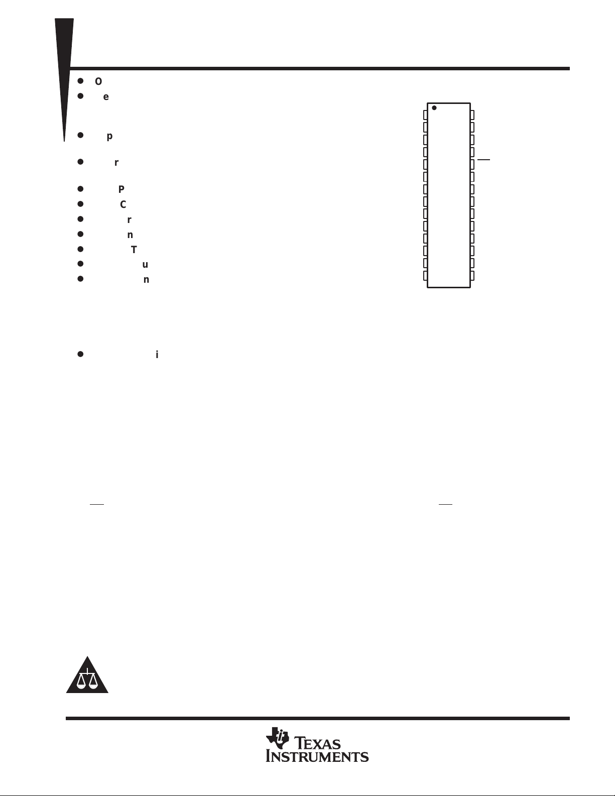
DB OR DW PACKAGE
(TOP VIEW)
TOUT3
TOUT1
TOUT2
RIN2
ROUT2
TIN2
TIN1
ROUT1
RIN1
GND
V
CC
C1+
V
DD
C1–
1
2
3
4
5
6
7
8
9
10
11
12
13
14
TOUT4
28
RIN3
27
ROUT3
26
SHUTDOWN
25
EN
24
RIN4
23
ROUT4
22
21
TIN4
20
TIN3
19
ROUT5
18
RIN5
17
V
SS
16
C2–
15
C2+
description
The SN75LBC241† is a low-power LinBiCMOS line-interface device containing four independent drivers and
five receivers. It is designed as a plug-in replacement for the Maxim MAX241. The SN75LBC241 provides a
capacitive-charge-pump voltage generator to produce RS-232 voltage levels from a 5-V supply. The
charge-pump oscillator frequency is 20 kHz. Each receiver converts RS-232 inputs to 5-V TTL/CMOS levels.
The receivers have a typical threshold of 1.2 V and a typical hysteresis of 0.5 V and can accept ±30-V inputs.
Each driver converts TTL/CMOS input levels into RS-232 levels.
The SN75LBC241 includes a receiver, a 3-state control line, and a low-power shutdown control line. When the
line is high, receiver outputs are placed in the high-impedance state. When EN is low, normal operation is
EN
enabled.
The shutdown mode reduces power dissipation to less than 5 µW typically . In this mode, receiver outputs have
high impedance, driver outputs are turned off, and the charge-pump circuit is turned off. When SHUTDOWN
is high, the shutdown mode is enabled. When SHUTDOWN is low, normal operation is enabled.
This device has been designed to conform to TIA/EIA-232-F and ITU Recommendation V.28.
The SN75LBC241 has been designed using LinBiCMOS technology and cells contained in the Texas
Instruments LinASIC library. Use of LinBiCMOS circuitry increases latch-up immunity in this device over an
all-CMOS design.
The SN75LBC241 is characterized for operation from 0°C to 70°C.
Please be aware that an important notice concerning availability, standard warranty, and use in critical applications of
Texas Instruments semiconductor products and disclaimers thereto appears at the end of this data sheet.
†
Patent pending
LinBiCMOS and LinASIC are trademarks of Texas Instruments Incorporated.
PRODUCTION DATA information is current as of publication date.
Products conform to specifications per the terms of Texas Instruments
standard warranty. Production processing does not necessarily include
testing of all parameters.
POST OFFICE BOX 655303 • DALLAS, TEXAS 75265
Copyright 1999, Texas Instruments Incorporated
1

SN75LBC241
LOW-POWER LinBiCMOS MULTIPLE DRIVERS AND RECEIVERS
SLLS137E – MA Y 1992 – REVISED JANUAR Y 1999
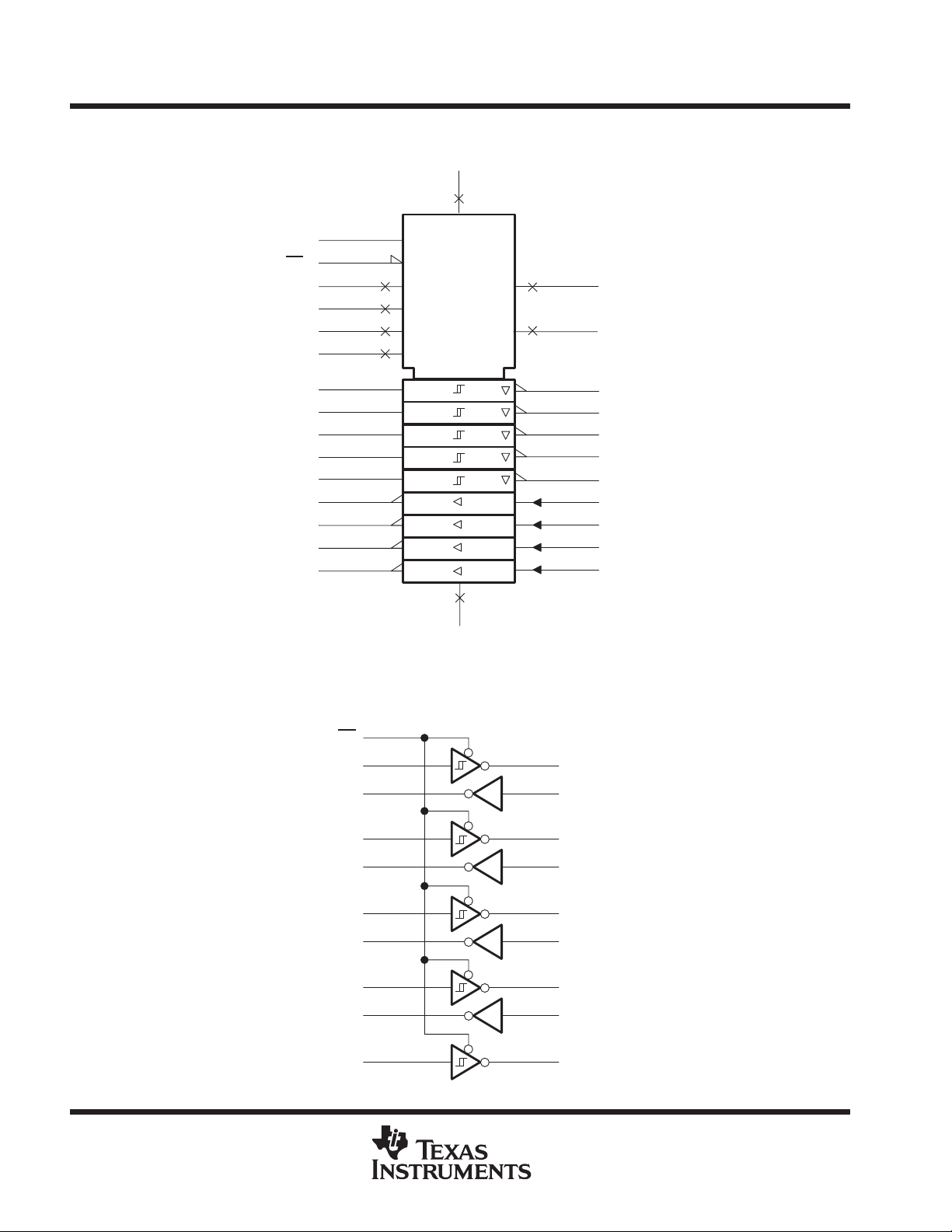
logic symbol
†
V
CC
11
SHUTDOWN
EN
C1+
C1–
C2+
C2–
RIN1
RIN2
RIN3
RIN4
RIN5
TOUT1
TOUT2
TOUT3
TOUT4
25
24
12
14
15
16
9
4
27
23
18
2
3
1
28
EN2
EN1
CX
CX
CX
CX
2
2
2
2
DRV/RCV
V
V
1,2
1,2
1,2
1,2
1,2
DD
SS
13
17
26
22
19
20
21
8
5
7
6
V
DD
V
SS
ROUT1
ROUT2
ROUT3
ROUT4
ROUT5
TIN1
TIN2
TIN3
TIN4
10
GND
†
This symbol is in accordance with ANSI/IEEE Std 91-1984 and IEC Publication 617-12.
logic diagram (positive logic)
24
EN
9
RIN1
RIN2
RIN3
RIN4
RIN5
2
4
3
27
1
23
28
TOUT1
TOUT2
TOUT3
TOUT4
26
20
22
21
1918
8
7
5
6
ROUT1
TIN1
ROUT2
TIN2
ROUT3
TIN3
ROUT4
TIN4
ROUT5
2
POST OFFICE BOX 655303 • DALLAS, TEXAS 75265

High-level input voltage, V
V
External charge-pump capacitor voltage rating
V
SN75LBC241
LOW-POWER LinBiCMOS MULTIPLE DRIVERS AND RECEIVERS
SLLS137E – MA Y 1992 – REVISED JANUAR Y 1999
absolute maximum ratings over operating free-air temperature range (unless otherwise noted)
Input supply voltage range, V
Positive output supply voltage range, V
Negative output supply voltage range, V
Input voltage range, V
: Driver –0.3 V to VCC + 0.3 V. . . . . . . . . . . . . . . . . . . . . . . . . . . . . . . . . . . . . . . . . . . . . . . .
I
Receiver ±30 V. . . . . . . . . . . . . . . . . . . . . . . . . . . . . . . . . . . . . . . . . . . . . . . . . . . . . . . . . . .
Output voltage range, V
O
Short-circuit duration: TOUT Unlimited. . . . . . . . . . . . . . . . . . . . . . . . . . . . . . . . . . . . . . . . . . . . . . . . . . . . . . . . . . . . .
Continuous total dissipation See Dissipation Rating Table. . . . . . . . . . . . . . . . . . . . . . . . . . . . . . . . . . . . . . . . . . .
Storage temperature range, T
Lead temperature 1,6 mm (1/16 inch) from case for 10 seconds 260°C. . . . . . . . . . . . . . . . . . . . . . . . . . . . . . .
†
Stresses beyond those listed under “absolute maximum ratings” may cause permanent damage to the device. These are stress ratings only, and
functional operation of the device at these or any other conditions beyond those indicated under “recommended operating conditions” is not
implied. Exposure to absolute-maximum-rated conditions for extended periods may affect device reliability.
NOTE 1: All voltage values are with respect to the network ground terminal.
PACKAGE
DB 1348 mW 10.8 mW/°C 862 mW
DW 1603 mW 12.8 mW/°C 1026 mW
(see Note 1) –0.3 V to 6 V. . . . . . . . . . . . . . . . . . . . . . . . . . . . . . . . . . . . . . . . . .
CC
V
DD
0.3 V to –15 V. . . . . . . . . . . . . . . . . . . . . . . . . . . . . . . . . . . . . . . . . . .
SS
CC
: TOUT VSS – 0.3 V to VDD + 0.3 V. . . . . . . . . . . . . . . . . . . . . . . . . . . . . . . . . . . . . . . .
ROUT –0.3 V to V
–65°C to 150°C. . . . . . . . . . . . . . . . . . . . . . . . . . . . . . . . . . . . . . . . . . . . . . . . . . .
stg
DISSIPATION RATING TABLE
TA ≤ 25°C
POWER RATING
OPERATING FACTOR
ABOVE TA = 25°C
TA = 70°C
POWER RATING
– 0.3 V to 15 V. . . . . . . . . . . . . . . . . . . . . . . . . . . . . . . . . . . . . .
+ 0.3 V. . . . . . . . . . . . . . . . . . . . . . . . . . . . . . . . . . . . . . . . . . . . .
CC
†
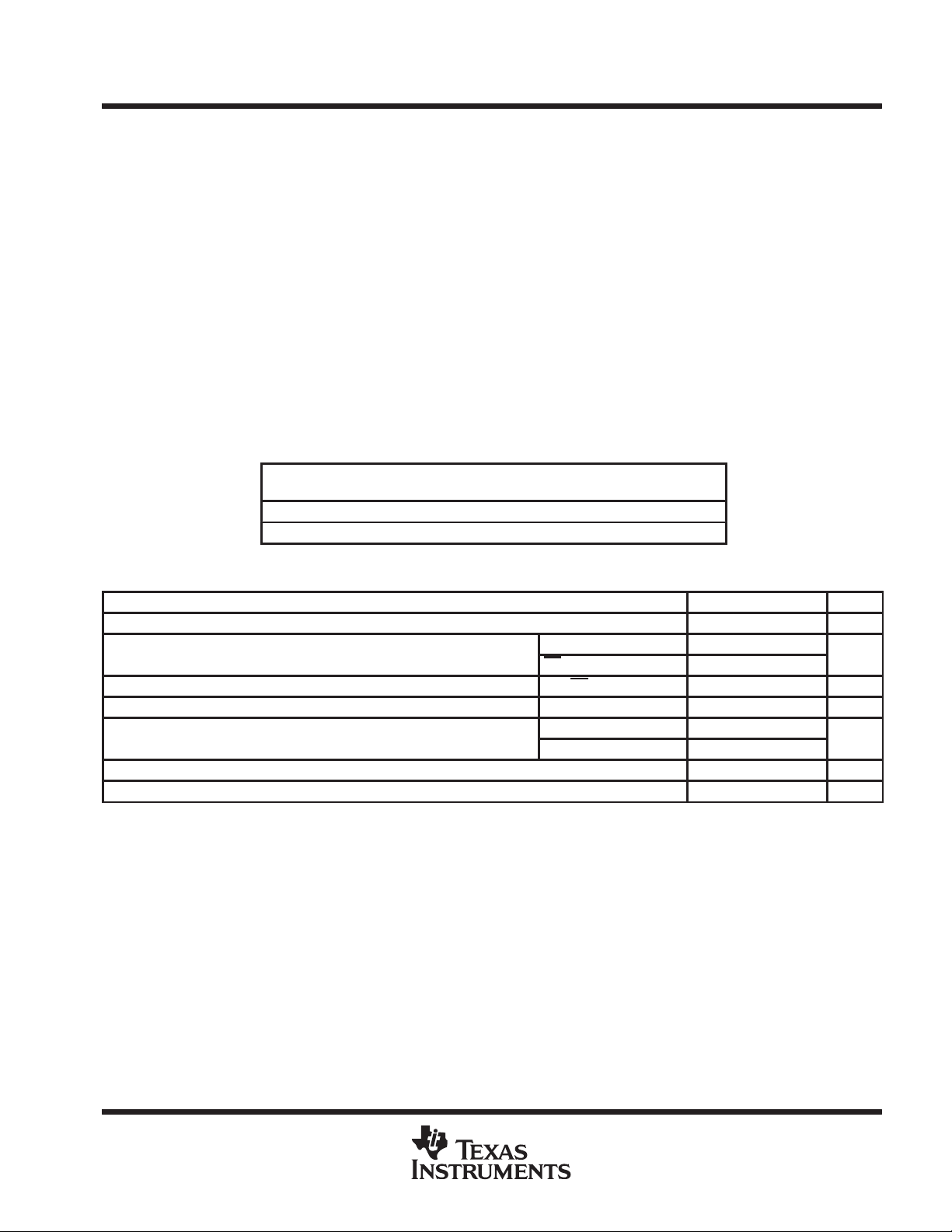
recommended operating conditions
MIN NOM MAX UNIT
Supply voltage, V
Low-level input voltage, V
External charge-pump capacitor C1–C4 (see Figure 1) 1 µF
Receiver input voltage, V
Operating free-air temperature, T
CC
p
p
IH
IL
p
p
I
A
TIN 2
EN, SHUTDOWN 2.4
TIN, EN, SHUTDOWN 0.8 V
C1, C3 (see Figure 1) 6.3
C2, C4 (see Figure 1) 16
4.5 5 5.5 V
±30 V
0 70 °C
POST OFFICE BOX 655303 • DALLAS, TEXAS 75265
3
 Loading...