

SN75LBC187
MULTICHANNEL EIA-232 DRIVER/RECEIVER
WITH CHARGE PUMP
SLLS130C – SEPTEMBER 1991 – REVISED MA Y 1995
1
POST OFFICE BOX 655303 • DALLAS, TEXAS 75265
D
Single IC and Single 5-V Supply Interface
for Serial Communication Ports
D
Meets or Exceeds the Requirements of
ANSI Standards EIA/TIA-232-E-1991,
EIA/TIA-562, and ITU Recommendation V.28
D
Switched-Capacitor Voltage Converter
Eliminates Need for ±12-V Supplies
D
Voltage Converter Operates With Low
Capacitance...0.1 µF Min
D
Designed for Data Rates up to 120 kb/s
Over 3-m Cable
D
Available in Shrink Small-Outline 25-milPitch Package
D
Shutdown Mode to Save Power When Not
in Use
D
±30-V Receiver Input Voltage Range
D
LinBiCMOS Process Technology
D
Applications
– Laptop or Notebook Computers
– Portable Terminals
– Single-Board Computers
– Portable Test Equipment
description
The SN75LBC187 is a low-power LinBiCMOS device containing three drivers, five receivers, and a
switched-capacitor voltage converter. The SN75LBC187 provides a single chip and single 5-V supply interface
between the asynchronous communications element and the serial port connector of the data terminal
equipment (DTE). This device has been designed to conform to ANSI Standards EIA/TIA-232-E, EIA/TIA-562,
and ITU recommendation V.28.
The switched-capacitor voltage converter of the SN75LBC187 uses four small external capacitors to generate
the positive and negative voltages required by EIA/TIA-232-E (and V.28) line drivers from a single 5-V input.
The drivers feature output slew-rate limiting to eliminate the need for external filter capacitors. The receivers
can accept±30 V without damage. The device also features a reduced power or shutdown mode that cuts the
quiescent power to the IC when not transmitting data between the CPU and peripheral.
The SN75LBC187 has been designed using LinBiCMOS technology and cells contained in the Texas
Instruments LinASIC library. The SN75LBC187 is characterized for operation from 0°C to 70°C.
NOTE:
This device includes circuit designs and process technologies that have patents pending.
Copyright 1995, Texas Instruments Incorporated
PRODUCTION DATA information is current as of publication date.
Products conform to specifications per the terms of Texas Instruments
standard warranty. Production processing does not necessarily include
testing of all parameters.
1
2
3
4
5
6
7
8
9
10
11
12
13
14
28
27
26
25
24
23
22
21
20
19
18
17
16
15
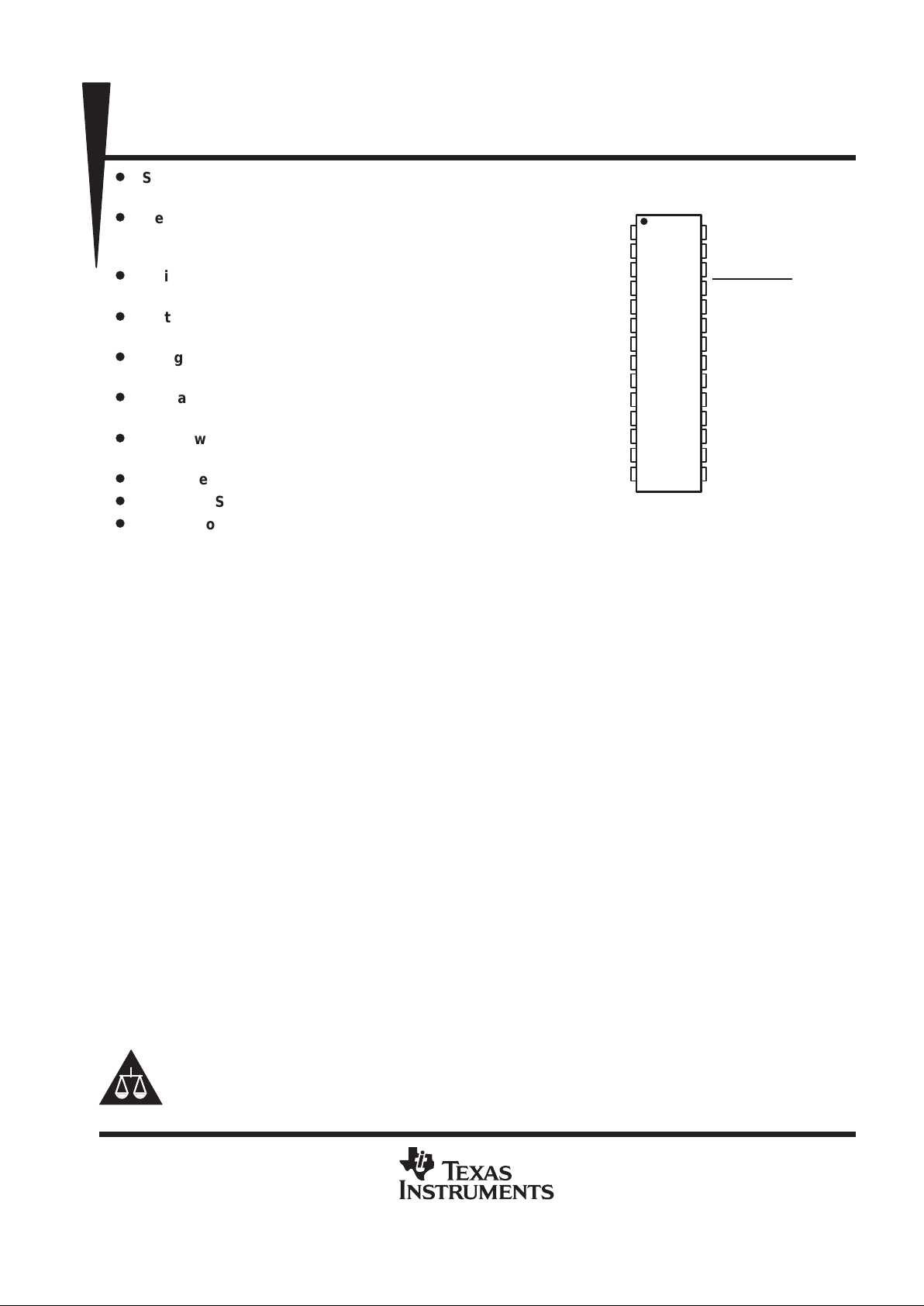
DY3
DY1
DY2
RA2
RY2
DA2
DA1
RY1
RA1
GND
V
CC
C1+
V
DD
C1–
NC
RA3
RY3
SHUTDOWN
NC
RA4
RY4
NC
DA3
RY5
RA5
V
SS
C2–
C2+
DB PACKAGE
(TOP VIEW)
NC–No internal connection
Please be aware that an important notice concerning availability, standard warranty, and use in critical applications of
Texas Instruments semiconductor products and disclaimers thereto appears at the end of this data sheet.
LinBiCMOS and LinASIC are a trademarks of Texas Instruments Incorporated.
SN75LBC187
MULTICHANNEL EIA-232 DRIVER/RECEIVER
WITH CHARGE PUMP
SLLS130C – SEPTEMBER 1991 – REVISED MA Y 1995
2
POST OFFICE BOX 655303 • DALLAS, TEXAS 75265
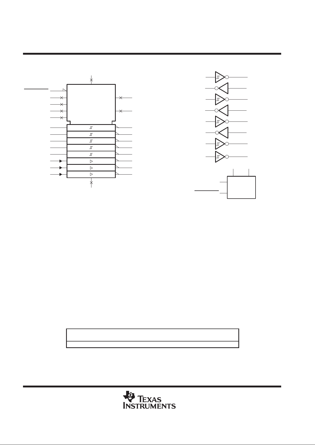
logic symbol
†
20
6
7
19
22
26
5
8
17
13
1
3
2
18
23
27
4
9
16
15
14
12
GND
DA3
DA2
DA1
RY5
RY4
RY3
RY2
RY1
V
SS
V
DD
DY3
DY2
DY1
RA5
RA4
RA3
RA2
RA1
C2–
C2+
C1–
C1+
SHUTDOWN
–2 VCC +1.5 V
2 VCC –1.5 V
C2–
C2+
C1–
C1+
[PWR DOWN]
V
CC
11
10
25
†
This symbol is in accordance with ANSI/IEEE Std. 91-1984 and
IEC Publication 617-12.
logic diagram (positive logic)
SHUTDOWN
V
CC
V
SS
V
DD
Circuit
Capacitor
Switched-
RA5
RA4
DY3
RA3
DY2
RA2
DY1
RA1
RY5
RY4
DA3
RY3
DA2
RY2
DA1
RY1
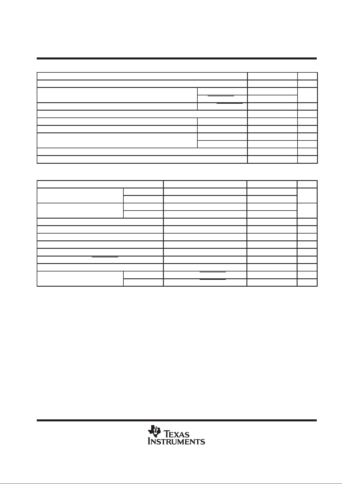
absolute maximum ratings over operating free-air temperature range (unless otherwise noted)
‡
Supply voltage range, V
CC
(see Note 1) 0.3 V to 6 V. . . . . . . . . . . . . . . . . . . . . . . . . . . . . . . . . . . . . . . . . . . . . . . .
Positive output supply voltage range, V
DD
V
CC
–0.3 V to 15 V. . . . . . . . . . . . . . . . . . . . . . . . . . . . . . . . . . . . . . .
Negative output supply voltage range, V
SS
0.3 V to –15 V. . . . . . . . . . . . . . . . . . . . . . . . . . . . . . . . . . . . . . . . . . .
Input voltage range, V
I
: RA ±30 V. . . . . . . . . . . . . . . . . . . . . . . . . . . . . . . . . . . . . . . . . . . . . . . . . . . . . . . . . . . . . . . .
All other inputs –0.3 V to V
CC
+ 3 V. . . . . . . . . . . . . . . . . . . . . . . . . . . . . . . . . . . . . . . . .
Output voltage range, V
O
:DY –2 VCC + 1.2 V to 2 VCC – 1.2 V. . . . . . . . . . . . . . . . . . . . . . . . . . . . . . . . . . . . . .
All other outputs –0.3 V to V
CC
+ 3 V. . . . . . . . . . . . . . . . . . . . . . . . . . . . . . . . . . . . . .
Continuous total power dissipation See Dissipation Rating Table. . . . . . . . . . . . . . . . . . . . . . . . . . . . . . . . . . . . .
Operating free-air temperature range, T
A
0°C to 70°C. . . . . . . . . . . . . . . . . . . . . . . . . . . . . . . . . . . . . . . . . . . . . .
Storage temperature range, T
stg
–65°C to 150°C. . . . . . . . . . . . . . . . . . . . . . . . . . . . . . . . . . . . . . . . . . . . . . . . . . .
Lead temperature 1,6 mm (1/16 inch) from case for 10 seconds 260°C. . . . . . . . . . . . . . . . . . . . . . . . . . . . . . .
‡
Stresses beyond those listed under “absolute maximum ratings” may cause permanent damage to the device. These are stress ratings only, and
functional operation of the device at these or any other conditions beyond those indicated under “recommended operating conditions” is not
implied. Exposure to absolute-maximum-rated conditions for extended periods may affect device reliability.
NOTE 1: All voltages are with respect to the network ground terminal.
DISSIPATION RATING TABLE
PACKAGE
TA ≤ 25°C
POWER RATING
DERATING FACTOR
ABOVE TA = 25°C
TA = 70°C
POWER RATING
DB 1025 mW 8.2 mW/°C 656 mW
SN75LBC187
MULTICHANNEL EIA-232 DRIVER/RECEIVER
WITH CHARGE PUMP
SLLS130C – SEPTEMBER 1991 – REVISED MA Y 1995
3
POST OFFICE BOX 655303 • DALLAS, TEXAS 75265
recommended operating conditions
MIN NOM MAX UNIT
Supply voltage, V
CC
4.5 5 5.5 V
p
DA 2
High-level input voltage, V
IH
RA, SHUTDOWN 2.4
V
Low-level input voltage, V
IL
RA, DA, SHUTDOWN 0.8 V
Receiver input voltage, V
I
–25 25 V
High-level output current, I
OH
RY –1 mA
Low-level output current, I
OL
RY 3.2 mA
p
V
DD
±10 µA
Output current, I
O
V
SS
±10 µA
C1, C2, C3, C4 charge pump capacitors 0.1 0.47 µF
Operating free-air temperature, T
A
0 70 °C
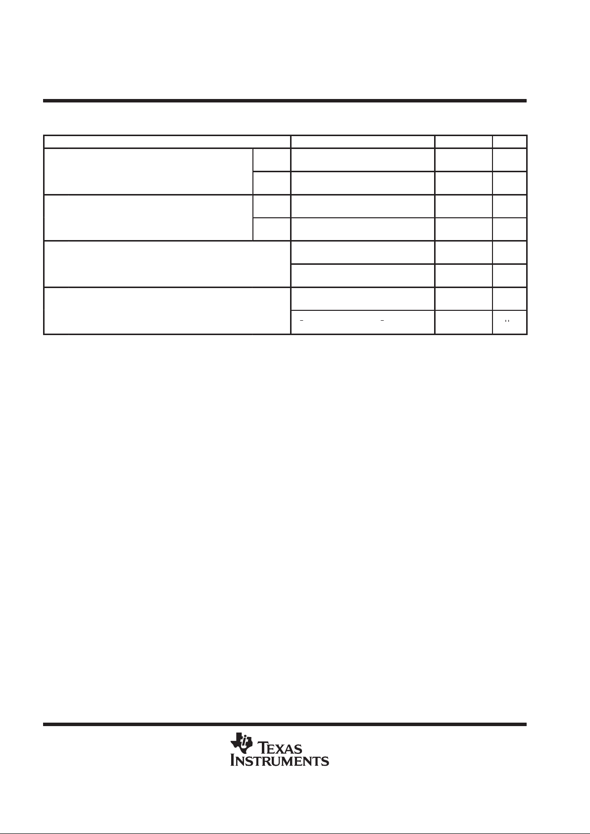
electrical characteristics over recommended operating conditions (unless otherwise noted)
PARAMETER TEST CONDITIONS MIN TYP†MAX UNIT
p
Receiver IO = –1 mA 3.5
VOHHigh-level output voltage
Driver RL = 3 kΩ to GND 5 7
V
p
Receiver IO = 3.2 mA 0.4
VOLLow-level output voltage
Driver RL = 3 kΩ to GND –7 –5
V
V
IT+
Receiver positive-going input voltage threshold 1.7 2.4 V
V
IT–
Receiver negative-going input voltage threshold 0.8 1.2 V
V
hys
Receiver input hysteresis voltage (V
IT+
– V
IT–
) 0.5 1 V
r
i
Receiver input resistance VCC = 5 V, TA = 25°C 3 5 7 kΩ
r
o
Driver output resistance VCC = 0, VO = ±2 V 300 Ω
I
I
Input current (DA, SHUTDOWN) VI = 0 to V
CC
±50 µA
I
OS
Driver output short-circuit current VO = 0 ±10 mA
pp
Normal operation All outputs open, SHUTDOWN at 2.4 V 15 30 mA
ICCSupply current
Shutdown mode All outputs open, SHUTDOWN at 0.1 V 10 µA
†
All typical values are at VCC = 5 V and TA = 25°C.
SN75LBC187
MULTICHANNEL EIA-232 DRIVER/RECEIVER
WITH CHARGE PUMP
SLLS130C – SEPTEMBER 1991 – REVISED MA Y 1995
4
POST OFFICE BOX 655303 • DALLAS, TEXAS 75265
switching characteristics over recommended operating conditions, TA = 25°C (unless otherwise
noted)
PARAMETER TEST CONDITIONS MIN MAX UNIT
p
p
Receiver
RL = 5 kΩ,
See Figure 1
CL = 50 pF,
1.25 µs
t
PLH
Propagation delay time, lo
w- to
high-level output
Driver
RL = 3 kΩ,
See Figure 2
CL = 1200 pF,
1.25 µs
p
p
Receiver
RL = 5 kΩ,
See Figure 1
CL = 50 pF,
1.25 µs
t
PHL
Propagation delay time, high- to low-level output
Driver
RL = 3 kΩ,
See Figure 2
CL = 1200 pF,
1.25 µs
p
RL = 3 kΩ,
VO = –3 V to 3 V ,
CL = 50 pF,
See Note 2
200 ns
trRise time, driver output
RL = 3 kΩ,
VO = –3.3 V to 3.3 V ,
CL = 2500 pF,
See Note 3
1.5 µs
p
RL = 3 kΩ,
VO = 3 V to –3 V
CL = 50 pF,
200 ns
tfFall time, driver output
RL = 3 kΩ, CL = 2500 pF,
L
VO = 3.3 V to –3.3 V
L
1.5µs
NOTES: 2. The 200 ns for the output to change from –3 V to 3 V (or vice versa) corresponds to the 30 V/µs maximum slew rate of EIA/TIA-232-E,
EIA/TIA-562, and ITU Recommendation V.28.
3. The more stringent requirement for transition times comes from the EIA/TIA-562, which requires the rise and fall times to be
measured from 3.3 V.

SN75LBC187
MULTICHANNEL EIA-232 DRIVER/RECEIVER
WITH CHARGE PUMP
SLLS130C – SEPTEMBER 1991 – REVISED MA Y 1995
5
POST OFFICE BOX 655303 • DALLAS, TEXAS 75265
PARAMETER MEASUREMENT INFORMATION
Output
(see Note B)
Input
V
OL
V
OH
10%
90%
–3 V
3 V
t
PHL
t
PLH
Output
I
O
V
CC
Input
V
IT, VI
V
O
5 kΩ
CL = 50 pF
(see Note A)
V
CC
1.5 kΩ
V
IH
V
IL
Figure 1. Receiver Test Circuit and Waveforms
–3 V
–3 V
3 V
3 V
t
r
t
f
0 V
3 V
50%50%
Output
Input
V
OH
t
PHL
t
PLH
Output
I
O
V
CC
Input
V
O
V
IT, VI
3 kΩ
V
OL
CL = 1200 pF
(see Note A)
NOTES: A. CL includes probe and jig capacitance.
B. The pulse generator has the following characteristics: tw = 8.33 µs, PRR = 60 kHz, tr = tf ≤ 50 ns.
Figure 2. Driver Test Circuit and Waveforms

SN75LBC187
MULTICHANNEL EIA-232 DRIVER/RECEIVER
WITH CHARGE PUMP
SLLS130C – SEPTEMBER 1991 – REVISED MA Y 1995
6
POST OFFICE BOX 655303 • DALLAS, TEXAS 75265
APPLICATION INFORMATION
EIA/TIA-232-E
DB9S
Connector
CS
DCD
DSR
RX
RTS
TX
CTS
DTR
RI
1
6
9
5
SN75LBC187
V
CC
RY1
RY2
RY3
DA1
DA2
RY4
DA3
RY5
GND
5 V
TL16C550
ACE
DCD
DSR
SI
RTS
SO
CTS
DTR
RI
SHUTDOWN C2 C2–
V
SS
RA1
RA2
RA3
DY1
DY2
RA4
DY3
RA5
V
DD
C1
0.1 µF
10 V
6.3 V
4.7 µF
C5
C1 C1–
+
10
19
20
22
6
7
26
5
8
11
13
18
1
23
3
2
27
4
9
17
25 15
16
1212 14
C3
0.1 µF
16 V
C4
0.1 µF
16 V
C2
0.1 µF
10 V
NOTE: C1, C2, C3, and C4 are Z5U-type ceramic-chip capacitors.
Figure 3. Typical SN75LBC187 Connection
SN75LBC187
MULTICHANNEL EIA-232 DRIVER/RECEIVER
WITH CHARGE PUMP
SLLS130C – SEPTEMBER 1991 – REVISED MA Y 1995
7
POST OFFICE BOX 655303 • DALLAS, TEXAS 75265
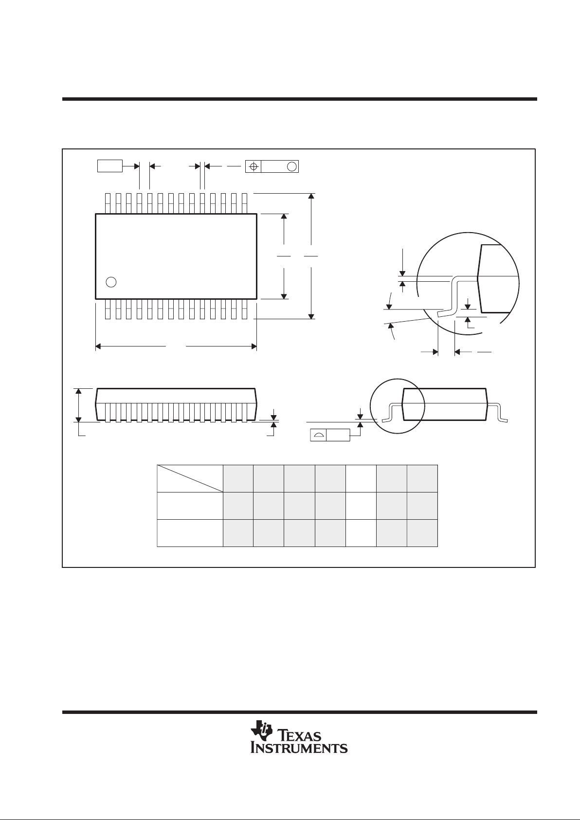
MECHANICAL DATA
DB (R-PDSO-G**) PLASTIC SMALL-OUTLINE PACKAGE
4040065 /D 02/98
28 PIN SHOWN
Gage Plane
8,20
7,40
0,15 NOM
0,63
1,03
0,25
38
12,90
12,30
28
10,50
24
8,50
Seating Plane
9,907,90
30
10,50
9,90
0,38
5,60
5,00
15
0,22
14
A
28
1
2016
6,50
6,50
14
0,05 MIN
5,905,90
DIM
A MAX
A MIN
PINS **
2,00 MAX
6,90
7,50
0,65
M
0,15
0°–8°
0,10
NOTES: A. All linear dimensions are in millimeters.
B. This drawing is subject to change without notice.
C. Body dimensions do not include mold flash or protrusion not to exceed 0,15.
D. Falls within JEDEC MO-150

IMPORTANT NOTICE
T exas Instruments and its subsidiaries (TI) reserve the right to make changes to their products or to discontinue
any product or service without notice, and advise customers to obtain the latest version of relevant information
to verify, before placing orders, that information being relied on is current and complete. All products are sold
subject to the terms and conditions of sale supplied at the time of order acknowledgement, including those
pertaining to warranty, patent infringement, and limitation of liability.
TI warrants performance of its semiconductor products to the specifications applicable at the time of sale in
accordance with TI’s standard warranty. Testing and other quality control techniques are utilized to the extent
TI deems necessary to support this warranty. Specific testing of all parameters of each device is not necessarily
performed, except those mandated by government requirements.
CERT AIN APPLICATIONS USING SEMICONDUCTOR PRODUCTS MAY INVOLVE POTENTIAL RISKS OF
DEATH, PERSONAL INJURY, OR SEVERE PROPERTY OR ENVIRONMENTAL DAMAGE (“CRITICAL
APPLICATIONS”). TI SEMICONDUCTOR PRODUCTS ARE NOT DESIGNED, AUTHORIZED, OR
WARRANTED TO BE SUITABLE FOR USE IN LIFE-SUPPORT DEVICES OR SYSTEMS OR OTHER
CRITICAL APPLICATIONS. INCLUSION OF TI PRODUCTS IN SUCH APPLICA TIONS IS UNDERST OOD TO
BE FULLY AT THE CUSTOMER’S RISK.
In order to minimize risks associated with the customer’s applications, adequate design and operating
safeguards must be provided by the customer to minimize inherent or procedural hazards.
TI assumes no liability for applications assistance or customer product design. TI does not warrant or represent
that any license, either express or implied, is granted under any patent right, copyright, mask work right, or other
intellectual property right of TI covering or relating to any combination, machine, or process in which such
semiconductor products or services might be or are used. TI’s publication of information regarding any third
party’s products or services does not constitute TI’s approval, warranty or endorsement thereof.
Copyright 1998, Texas Instruments Incorporated
 Loading...