

SN65LBC171, SN75LBC171
TRIPLE DIFFERENTIAL TRANSCEIVERS
SLLS460A – NOVEMBER 2000 – REVISED FEBRUARY 2001
D
Three Differential Transceivers in One
Package
D
Signaling Rates1 Up to 30 Mbps
D
Low Power and High Speed
D
Designed for TIA/EIA-485, TIA/EIA-422, ISO
8482, and ANSI X3.277 (HVD SCSI Fast–20)
Applications
D
Common-Mode Bus Voltage Range
–7 V to 12 V
D
ESD Protection on Bus Terminals
Exceeds 12 kV
D
Driver Output Current up to ±60 mA
D
Thermal Shutdown Protection
D
Driver Positive and Negative Current
Limiting
D
Power-Up, Power-Down Glitch-Free
Operation
D
Pin-Compatible With the SN75ALS171
D
Available in Shrink Small-Outline Package
description
The SN65LBC171 and SN75LBC171 are
monolithic integrated circuits designed for
bidirectional data communication on multipoint
bus-transmission lines. Potential applications
include serial or parallel data transmission, cabled
peripheral buses with twin axial, ribbon, or
twisted-pair cabling. These devices are suitable
for FAST–20 SCSI and can transmit or receive
data pulses as short as 25 ns, with skew less than
3 ns.
These devices combine three 3-state differential
line drivers and three differential input line
receivers, all of which operate from a single 5-V
power supply.
SN65LBC171DB (Marked as BL171)
SN75LBC171DB (Marked as LB171)
SN65LBC171DW (Marked as 65LBC171)
SN75LBC171DW (Marked as 75LBC171)
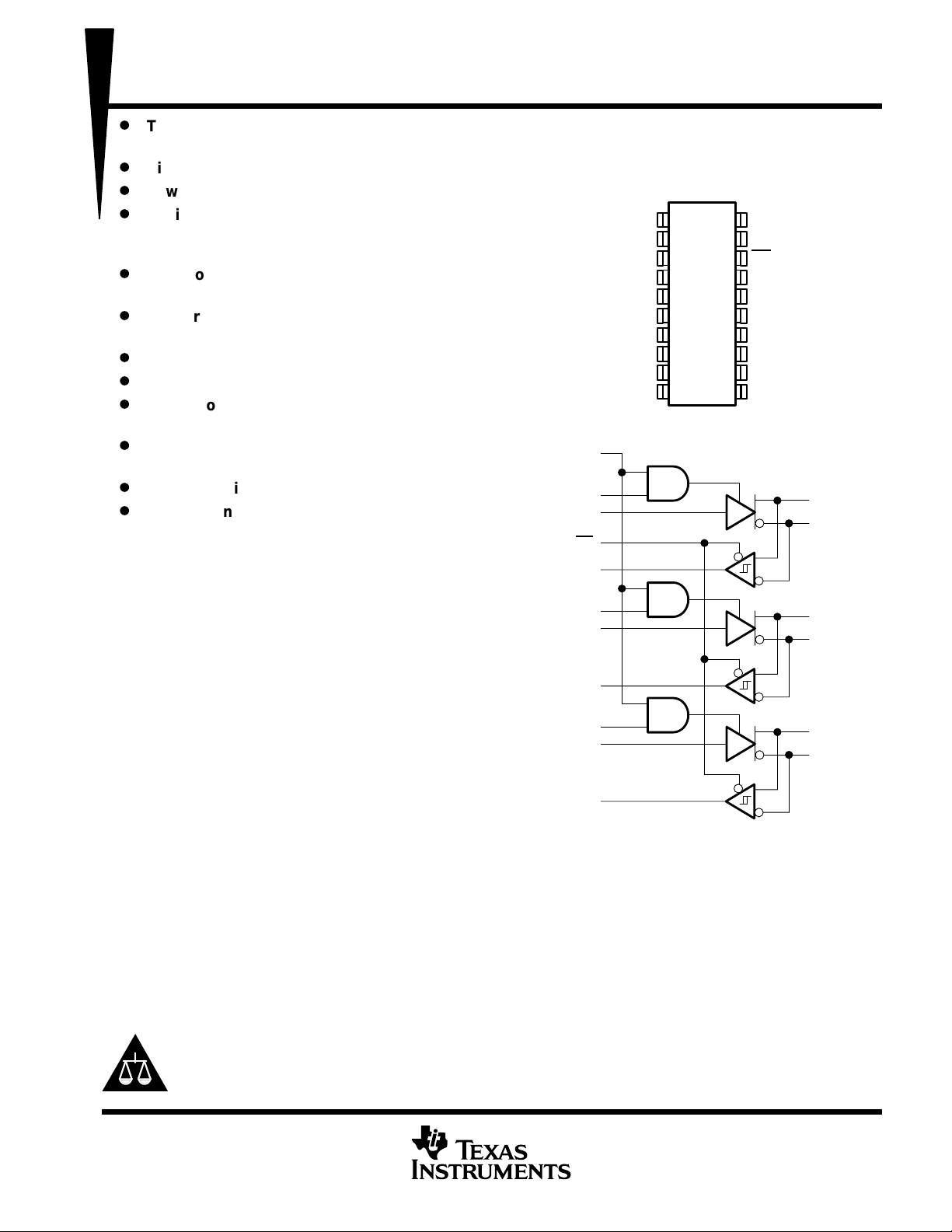
logic diagram
CDE
1DE
1D
RE
1R
2DE
2D
2R
3DE
3D
3R
1R
1DE
1D
GND
GND
2R
2DE
2D
3R
3DE
(TOP VIEW)
1
20
2
19
3
18
4
17
5
16
6
15
7
14
8
13
9
12
10
11
1B
1A
RE
CDE
V
CC
2B
2A
3B
3A
3D
1A
1B
2A
2B
3A
3B
The driver differential outputs and the receiver differential inputs are connected internally to form three
differential input/output (I/O) bus ports that are designed to offer minimum loading to the bus whenever the driver
is disabled or V
= 0. These ports feature a wide common-mode voltage range making the device suitable for
CC
party-line applications over long cable runs.
The SN75LBC171 is characterized for operation over the temperature range of 0°C to 70°C. The SN65LBC171
is characterized for operation over the temperature range of –40°C to 85°C.
Please be aware that an important notice concerning availability, standard warranty, and use in critical applications of
Texas Instruments semiconductor products and disclaimers thereto appears at the end of this data sheet.
1
The signaling rate of a line is the number of voltage transitions that are made per second expressed in the units bps (bits per second).
PRODUCTION DATA information is current as of publication date.
Products conform to specifications per the terms of Texas Instruments
standard warranty. Production processing does not necessarily include
testing of all parameters.
POST OFFICE BOX 655303 • DALLAS, TEXAS 75265
Copyright 2001, Texas Instruments Incorporated
1
SN65LBC171, SN75LBC171
TRIPLE DIFFERENTIAL TRANSCEIVERS
SLLS460A – NOVEMBER 2000 – REVISED FEBRUARY 2001
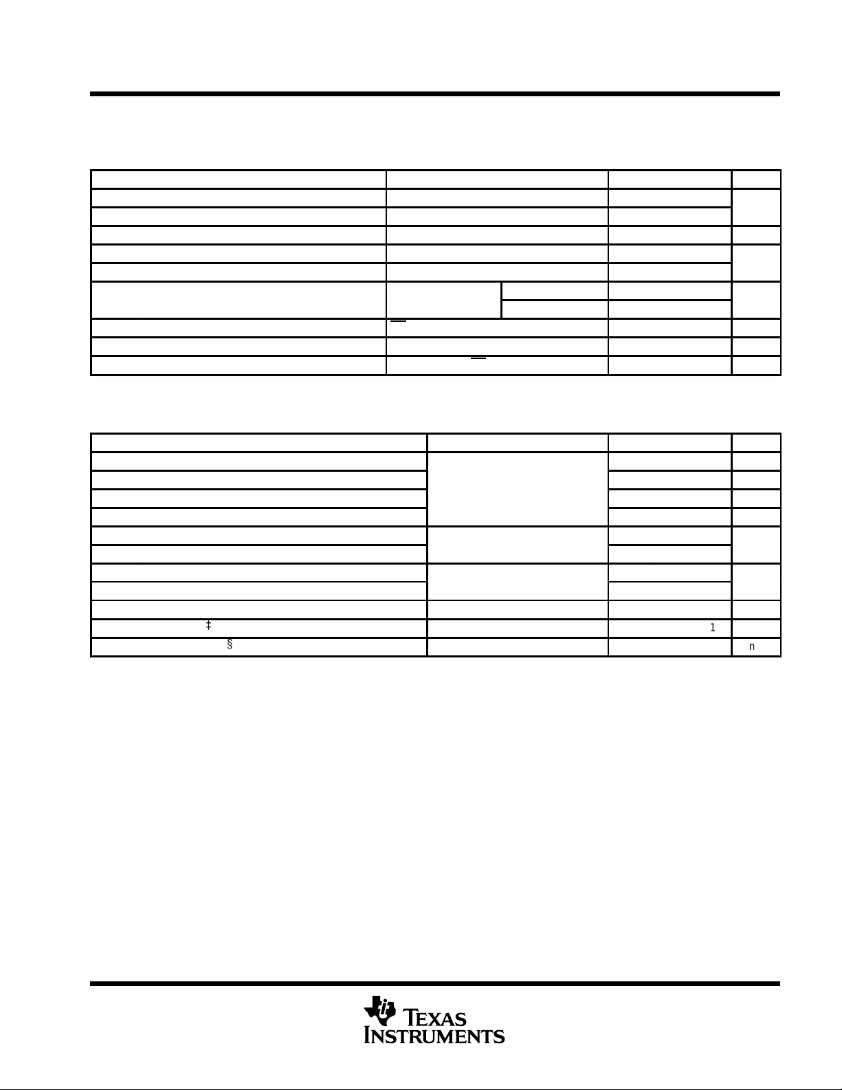
AVAILABLE OPTIONS
T
A
PLASTIC SMALL-OUTLINE
(JEDEC MS-013)
0°C to 70°C SN75LBC171DW SN75LBC171DB
–40°C to 85°C SN65LBC171DW SN65LBC171DB
†
Add R suffix for taped and reel
Function Tables
EACH DRIVER
INPUT
D
H
L
OPEN
X
X
X
X
ENABLE
DE CDE
H
H
H
L
X
OPEN
X
OPEN
H
H
H
X
L
X
OUTPUTS
A
B
H
L
L
H
L
H
Z
Z
Z
Z
Z
Z
Z
Z
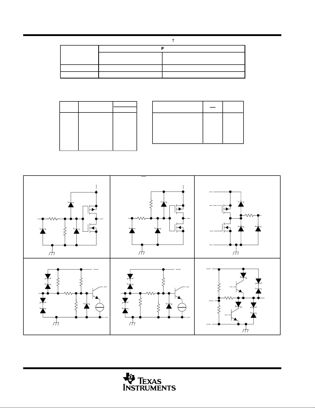
equivalent input and output schematic diagrams
D, DE,CDE INPUTS
V
CC
RE INPUT
{
PACKAGE
PLASTIC SHRINK SMALL-OUTLINE
(JEDEC MO-150)
EACH RECEIVER
DIFFERENTIAL INPUT
(VA–VB)
ENABLE
OUTPUT
RE
VID ≥ 0.2 V L H
–0.2 V < VID < 0.2 V L ?
VID ≤ –0.2 V L L
XHZ
OPEN
LH
H = high level, L = low level, X = irrelevant,
Z = high impedance (off), ? = indeterminate
V
CC
R OUTPUT
R
Input
Input
8 V
16 V
1 kΩ
100 kΩ
16 V
A INPUT
100 kΩ
18 kΩ
4 kΩ
4 kΩ
V
CC
100 kΩ
40 Ω
16 V
Output
Output
16 V
16 V
1 kΩ
8 V
B INPUT
18 kΩ
100 kΩ
4 kΩ
4 kΩ
A AND B OUTPUT
V
V
CC
CC
4 kΩ
18 kΩ
4 kΩ
Input
V
CC
16 V
Input
2
POST OFFICE BOX 655303 • DALLAS, TEXAS 75265
DE, CDE, RE
V
Output current
mA
Operating free-air temperature, T
°C
SN65LBC171, SN75LBC171
TRIPLE DIFFERENTIAL TRANSCEIVERS
SLLS460A – NOVEMBER 2000 – REVISED FEBRUARY 2001
absolute maximum ratings
Supply voltage, V
CC
†
(see Note 1) –0.3 V to 6 V. . . . . . . . . . . . . . . . . . . . . . . . . . . . . . . . . . . . . . . . . . . . . . . . . . . . . . . . . .
Voltage range at any bus I/O terminal (steady state) –10 V to 15 V. . . . . . . . . . . . . . . . . . . . . . . . . . . . . . . . . . .
Voltage input range, A and B, (transient pulse through 100 Ω, see Figure 12) –30 V to 30 V. . . . . . . . . . . . . .
Voltage range at any DE, RE
, or CDE terminal – 0.5 V to V
CC
+ 0.5 V. . . . . . . . . . . . . . . . . . . . . . . . . . . . . . . .
Electrostatic discharge: Human body model (A, B, GND) (see Note 2) 12 kV. . . . . . . . . . . . . . . . . . . . . . . . . .
All pins 5 kV. . . . . . . . . . . . . . . . . . . . . . . . . . . . . . . . . . . . . . . . . . . . . . . . . . . . . . . . . . . . . .
Charged-device model (all pins) (see Note 3) 1 kV. . . . . . . . . . . . . . . . . . . . . . . . . . . . .
Continuous total power dissipation See Power Dissipation Rating Table
Storage temperature range, T
. . . . . . . . . . . . . . . . . . . . . . . . . . . . . . . . . . .
stg
–65°C to 150°C. . . . . . . . . . . . . . . . . . . . . . . . . . . . . . . . . . . . . . . . . . . . . . . . . . . . . . . . .
Lead temperature 1,6 mm (1/16 inch) from case for 10 seconds 260°C. . . . . . . . . . . . . . . . . . . . . . . . . . . . . . . .
†
Stresses beyond those listed under “absolute maximum ratings” may cause permanent damage to the device. These are stress ratings only, and
functional operation of the device at these or any other conditions beyond those indicated under “recommended operating conditions” is not
implied. Exposure to absolute-maximum-rated conditions for extended periods may affect device reliability.
NOTES: 1. All voltage values, except differential I/O bus voltages, are with respect to network ground terminal.
2. Tested in accordance with JEDEC Standard 22, Test Method A114–A.
3. Tested in accordance with JEDEC Standard 22, Test Method C101.
POWER DISSIPATION RATING TABLE
PACKAGE
DB 995 mW 8.0 mW/°C 635 mW 515 mW
DW 1480 mW 11.8 mW/°C 950 mW 770 mW
‡
This is the inverse of the junction-to-ambient thermal resistance when board-mounted and with no air flow.
TA ≤ 25°C
POWER RATING
DERATING FACTOR
ABOVE TA = 25°C
‡
TA = 70°C
POWER RATING
TA = 85°C
POWER RATING
recommended operating conditions
MIN NOM MAX UNIT
Supply voltage, V
Voltage at any bus I/O terminal A, B –7 12 V
High-level input voltage, V
Low-level input voltage, V
Differential input voltage, V
p
p
CC
IH
IL
ID
p
A
A with respect to B –12 12 V
Driver –60 60
Receiver –8 8
SN75LBC171 0 70
SN65LBC171 –40 85
4.75 5 5.25 V
2 V
0 0.8
CC
POST OFFICE BOX 655303 • DALLAS, TEXAS 75265
3
SN65LBC171, SN75LBC171
(SS)
‡
()
magnitude
‡
C
L
F
R
54 Ω
C
50 pF
See Figure 3
S
(HVD SCSI double-terminated load)
See Figure 5
ns
See Figure 6
ns
TRIPLE DIFFERENTIAL TRANSCEIVERS
SLLS460A – NOVEMBER 2000 – REVISED FEBRUARY 2001
DRIVER SECTION
electrical characteristics over recommended operating conditions
PARAMETER TEST CONDITIONS MIN TYP†MAX UNIT
V
IK
V
O
|V
OD
∆V
OD
V
OC(SS)
∆V
OC(SS)
I
I
I
O
I
OS
I
CC
†
All typical values are at VCC = 5 V and TA = 25°C.
‡
The minimum VOD may not fully comply with TIA/EIA-485-A at operating temperatures below 0°C. System designers should take the possibly
lower output signal into account in determining the maximum signal-transmission distance.
Input clamp voltage D, DE, CDE II = 18 mA –1.5 –0.7 V
Open-circuit output voltage (single-ended) A or B, No load 0 V
Steady-state differential output voltage
|
Change in differential output voltage
magnitude, | V
Steady-state common-mode output voltage
Change in steady-state common-mode
output voltage (V
Input current D, DE, CDE –100 100 µA
Output current with power off VCC = 0 V, VO = –7 V to 12 V –700 900 µA
Short-circuit output current VO = –7 V to 12 V, See Figure 7 –250 250 mA
Supply current (driver enabled) D at 0 V or VCC,
OD(H)
OC(H)
| – |V
– V
OD(L)
OC(L)
|
)
No load 3.8 4.3 V
RL = 54 Ω, See Figure 1 1 1.6 2.4 V
With common-mode loading, See Figure 2 1 1.6 2.4 V
–0.2 0.2 V
RL = 54 Ω,
= 50
p
See Figure 1
CDE, DE, RE at
VCC, No load
2 2.4 2.8 V
–0.2 0.2 V
14 20 mA
CC
CC
V
V
switching characteristics over recommended operating conditions
PARAMETER TEST CONDITIONS MIN TYP MAX UNIT
t
PLH
t
PHL
t
r
t
f
t
sk(p)
t
sk(o)
t
sk(pp)
t
PLH
t
PHL
t
r
t
f
t
sk(p)
t
sk(o)
t
sk(pp)
t
PZH
t
PHZ
t
PZL
t
PLZ
§
Output skew (t
¶
Part-to-part skew (t
both devices operate with the same input signals, the same supply voltages, at the same temperature, and have identical packages and test
circuits.
Differential output propagation delay, low-to high 4 8.5 12
Differential output propagation delay, high-to-low 4 8.5 11
Differential output rise time
Differential output fall time
Pulse skew | (t
Output skew
Part-to-part skew
Differential output propagation delay, low-to high 3 7 10
Differential output propagation delay, high-to-low 3 7.5 10
Differential output rise time
Differential output fall time
Pulse skew | (t
Output skew
Part-to-part skew
Output enable time to high level
Output disable time from high level
Output enable time to low level
Output disable time from low level
) is the magnitude of the time delay difference between the outputs of a single device with all of the inputs connected together.
sk(o)
sk(pp)
– t
– t
PHL
PHL
) |
) |
PLH
§
¶
PLH
§
¶
) is the magnitude of the difference in propagation delay times between any specified terminals of two devices when
L
ee Figure 4,
=
,
L
-
=
,
3 7.5 11
3
7.5 11
1.5
3 7.5 12
3 7.5 12
1.5
2.5
15 25
18 25
10 25
17 25
ns
2
2
ns
3
4
POST OFFICE BOX 655303 • DALLAS, TEXAS 75265
V
V
IILine input current
Other input
V
mA
V
3 V to 3 V, See Figure 9
See Figure 10
ns
See Figure 11
ns
TRIPLE DIFFERENTIAL TRANSCEIVERS
SLLS460A – NOVEMBER 2000 – REVISED FEBRUARY 2001
RECEIVER SECTION
electrical characteristics over recommended operating conditions
PARAMETER TEST CONDITIONS MIN TYP†MAX UNIT
V
IT+
V
IT–
V
hys
V
OH
V
OL
I
I
R
I
I
CC
†
All typical values are at VCC = 5 V and TA = 25°C.
switching characteristics over recommended operating conditions
Positive-going differential input voltage threshold 0.2
Negative-going differential input voltage threshold –0.2
Hysteresis voltage (V
High-level output voltage VID = 200 mV, IOH = –8 mA, see Figure 10 4 4.7 V
Low-level output voltage VID = –200 mV , IOL = –8 mA, see Figure 10 0 0.2 0.4
p
Input current RE –100 100 µA
Input resistance A, B 12 kΩ
Supply current (receiver enabled) A, B, D open, RE, DE, and CDE at 0 V 16 mA
IT+
– V
) 40 mV
IT–
p
= 0
VI = 12 V 0.9
VI = –7 V –0.7
SN65LBC171, SN75LBC171
CC
PARAMETER TEST CONDITIONS MIN TYP MAX UNIT
t
PLH
t
PHL
t
r
t
f
t
PZH
t
PHZ
t
PZL
t
PLZ
t
sk(p)
t
sk(o)
t
sk(pp)
‡
Output skew (t
§
Part-to-part skew (t
both devices operate with the same input signals, the same supply voltages, at the same temperature, and have identical packages and test
circuits.
Propagation delay time, low-to-high level output 7 16 ns
Propagation delay time, high-to-low level output
Receiver output rise time
Receiver output fall time 1.3 3 ns
Receiver output enable time to high level
Receiver output disable time from high level
Receiver output enable time to low level
Receiver output enable time to high level
Pulse skew (| ( t
Output skew
Part-to-part skew
) is the magnitude of the time delay difference between the outputs of a single device with all of the inputs connected together.
sk(o)
sk(pp)
– t
PLH
}
w
) is the magnitude of the difference in propagation delay times between any specified terminals of two devices when
|) 2 ns
PHL
= –
ID
7 16 ns
1.3 3 ns
26 40
40
29 40
40
1.5 ns
3 ns
POST OFFICE BOX 655303 • DALLAS, TEXAS 75265
5
SN65LBC171, SN75LBC171
TRIPLE DIFFERENTIAL TRANSCEIVERS
SLLS460A – NOVEMBER 2000 – REVISED FEBRUARY 2001
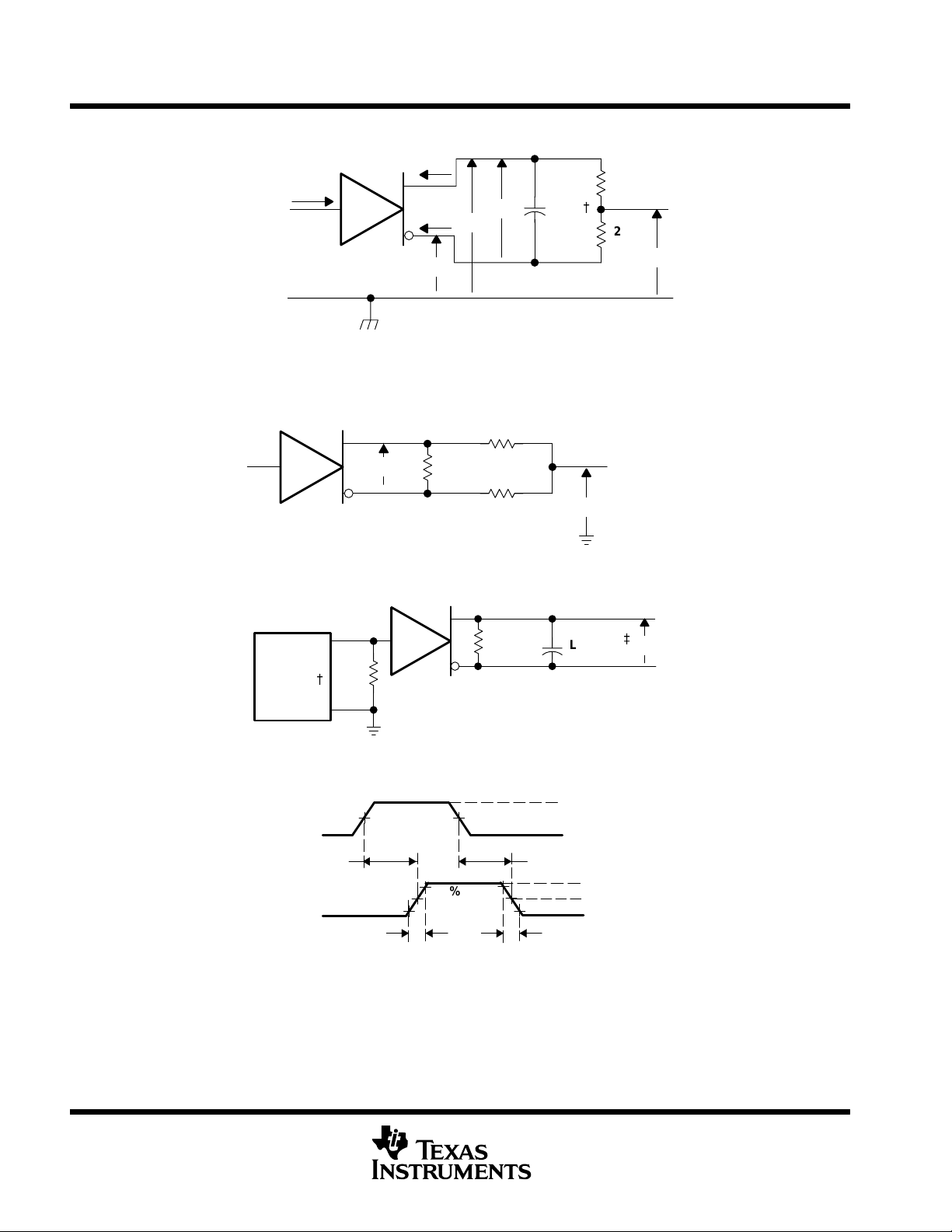
PARAMETER MEASUREMENT INFORMATION
I
I
0 V or 3 V
†
Includes probe and jig capacitance
Figure 1. Driver Test Circuit, VOD and VOC Without Common-Mode Loading
I
O
27 Ω
V
I
O
V
O
OD
V
O
375 Ω
50 pF
{
27 Ω
V
OC
Input
V
OD
60 Ω
375 Ω
V
TEST
V
TEST
Figure 2. Driver Test Circuit, VOD With Common-Mode Loading
RL = 54 Ω
Signal
Generator
† PRR = 1 MHz, 50% Duty Cycle, tr < 6 ns, tf < 6 ns, Zo = 50 Ω
‡ Includes Probe and Jig Capacitance
Input
Output
{
t
PLH
50 Ω
1.5 V
10%
t
r
90%
1.5 V
90%
t
PHL
10%
t
f
CL = 50 pF
3 V
0 V
V
OD(H)
0 V
V
OD(L)
}
= –7 V to 12 V
V
OD
Figure 3. Driver Switching Test Circuit and Waveforms, 485-Loading
6
POST OFFICE BOX 655303 • DALLAS, TEXAS 75265

SN65LBC171, SN75LBC171
TRIPLE DIFFERENTIAL TRANSCEIVERS
SLLS460A – NOVEMBER 2000 – REVISED FEBRUARY 2001
PARAMETER MEASUREMENT INFORMATION
5 V
0 V
Signal
Generator
† PRR = 1 MHz, 50% Duty Cycle, tr < 6 ns, tf < 6 ns, Zo = 50 Ω
‡ Includes Probe and Jig Capacitance
50 Ω
{
5 V
0 V
165 Ω
165 Ω
S1
S2
375 Ω
75 Ω
375 Ω
60 pF
V
OD
60 pF
}
Input
t
PLH
Output
}
1.5 V
10%
t
r
90%
1.5 V
90%
Figure 4. Driver Switching Test Circuit and Waveforms, HVD SCSI-Loading (double terminated)
0 V or 3 V
A
{
B
S1
CL = 50 pF
Output
w
RL = 110 Ω
t
PHL
10%
3 V
0 V
V
OD(H)
0 V
V
OD(L)
t
f
Input
Generator
† 3 V if testing A output, 0 V if testing B output
‡ PRR = 1 MHz, 50% Duty Cycle, tr < 6 ns, tf < 6 ns, Zo = 50 Ω
w
Includes Probe and Jig Capacitance
}
Input
Output
t
PZH
50 Ω
1.5 V
2.3 V
1.5 V
Figure 5. Driver Enable/Disable Test, High Output
0.5 V
t
PHZ
3 V
0 V
V
0 V
OH
POST OFFICE BOX 655303 • DALLAS, TEXAS 75265
7

SN65LBC171, SN75LBC171
TRIPLE DIFFERENTIAL TRANSCEIVERS
SLLS460A – NOVEMBER 2000 – REVISED FEBRUARY 2001
PARAMETER MEASUREMENT INFORMATION
5 V
A
0 V or 3 V
Generator
† 0 V if testing A output, 3 V if testing B output
‡ PRR = 1 MHz, 50% Duty Cycle, tr < 6 ns, tf < 6 ns, Zo = 50 Ω
w
Includes Probe and Jig Capacitance
{
B
Input
}
50 Ω
S1
RL = 110 Ω
CL = 50 pF
Figure 6. Driver Enable/Disable Test, Low Output
I
OS
V
O
Voltage
Source
Output
w
Input
t
Output
PZH
t
PHZ
0.5 V
3 V
0 V
5 V
V
OL
1.5 V
2.3 V
V
ID
1.5 V
I
O
V
O
Figure 7. Driver Short-Circuit Test
Generator
Generator
† PRR = 1 MHz, 50% Duty Cycle, tr < 6 ns, tf < 6 ns, Zo = 50 Ω
‡ Includes Probe and Jig Capacitance
{
50 Ω
A
V
ID
B
{
50 Ω
CL = 15 pF
I
O
R
‡
Figure 9. Receiver Switching Test Circuit and Waveforms
Figure 8. Receiver DC Parameters
Input B
Input A
t
V
O
PLH
Output
1.5 V
90% 90%
t
r
1.5 V1.5 V
t
PHL
10%10%
3 V
0 V
V
OH
V
OL
t
f
8
POST OFFICE BOX 655303 • DALLAS, TEXAS 75265

PARAMETER MEASUREMENT INFORMATION
1.5 V
Generator
† PRR = 1 MHz, 50% Duty Cycle, tr < 6 ns, tf < 6 ns, Zo = 50 Ω
‡ Includes Probe and Jig Capacitance
–1.5 V
Generator
A
R
B
EN
{
50 Ω
CL = 15 pF
1 kΩ
}
Figure 10. Receiver Enable/Disable Test, High Output
A
R
B
{
50 Ω
EN
CL = 15 pF
1 kΩ
}
SN65LBC171, SN75LBC171
TRIPLE DIFFERENTIAL TRANSCEIVERS
SLLS460A – NOVEMBER 2000 – REVISED FEBRUARY 2001
V
CC
3 V
1.5 V
t
PZH
1.5 V
V
CC
1.5 V
t
PZL
1.5 V
1.5 V
1.5 V
t
PHZ
VOH –0.5 V
t
PLZ
VOL + 0.5 V
0 V
V
GND
3 V
0 V
V
V
OH
CC
OL
† PRR = 1 MHz, 50% Duty Cycle, tr < 6 ns, tf < 6 ns, Zo = 50 Ω
‡ Includes Probe and Jig Capacitance
Figure 11. Receiver Enable/Disable Test, Low Output
100 Ω
Pulse
Generator,
15-µs Duration,
1% Duty Cycle
Figure 12. Test Circuit and Waveform, Transient Over Voltage Test
V
0 V
15 µs
TEST
1.5 ms
–V
TEST
POST OFFICE BOX 655303 • DALLAS, TEXAS 75265
9
SN65LBC171, SN75LBC171
TRIPLE DIFFERENTIAL TRANSCEIVERS
SLLS460A – NOVEMBER 2000 – REVISED FEBRUARY 2001
TYPICAL CHARACTERISTICS
DIFFERENTIAL OUTPUT VOLTAGE
vs
OUTPUT CURRENT
4
3.5
3
2.5
2
1.5
– Differential Output Voltage – V
1
OD
V
0.5
0
0 20406080100
VCC = 5.25 V
VCC = 5 V
VCC = 4.75 V
IO – Output Current – mA
Figure 13
DRIVER PROPAGATION DELAY
vs
FREE-AIR TEMPERATURE
12
11
10
9
SCSI Load
DIFFERENTIAL OUTPUT VOLTAGE
vs
FREE-AIR TEMPERATURE
2.5
2
VCC = 5 V
1.5
1
– Differential Output Voltage – V
0.5
OD
V
0
–60 –40 –20 0 20 40 60 80 100
TA – Free-Air Temperature – °C
VCC = 5.25 V
VCC = 4.75 V
Figure 14
SUPPLY CURRENT
vs
SIGNALING RATE
165
All 3 Channels Driving
RL = 54 Ω,
CL = 50 pF (Each Channel),
160
Pseudorandom NRZ Data
155
10
8
7
6
Driver Propagation Delay – ns
5
4
–40 –20020406080
TA – Free-Air Temperature – °C
RS–485 Load
Figure 15
POST OFFICE BOX 655303 • DALLAS, TEXAS 75265
150
145
– Supply Current – mA
CC
I
140
135
0.1 1 10 100
Signaling Rate – Mbps
Figure 16

SN65LBC171, SN75LBC171
TRIPLE DIFFERENTIAL TRANSCEIVERS
SLLS460A – NOVEMBER 2000 – REVISED FEBRUARY 2001
TYPICAL CHARACTERISTICS
BUS INPUT CURRENT
vs
BUS INPUT VOLTAGE
800
600
VCC = 0 V
400
Aµ
200
0
Bus Input Current –
–200
–400
–600
–10 –5051015
Bus Input Voltage – V
VCC = 5 V
Figure 17
SN65LBC171
(as Driver)
Signal
Generator
12
11
10
9
8
7
6
5
– Receiver Propagation Delay Time – ns
pd
t
4
–40 –20 0 20 40 60 80
15 Meters, Cat. 5
Twisted-Pair Cable
100 Ω
RECEIVER PROPAGATION DELAY TIME
vs
FREE-AIR TEMPERATURE
t
PHL
t
PLH
TA – Free-Air Temperature °C
Figure 18
SN65LBC171
(as Receiver)
15 pF
Figure 19. Circuit Diagram for Signaling Characteristics
POST OFFICE BOX 655303 • DALLAS, TEXAS 75265
11

SN65LBC171, SN75LBC171
TRIPLE DIFFERENTIAL TRANSCEIVERS
SLLS460A – NOVEMBER 2000 – REVISED FEBRUARY 2001
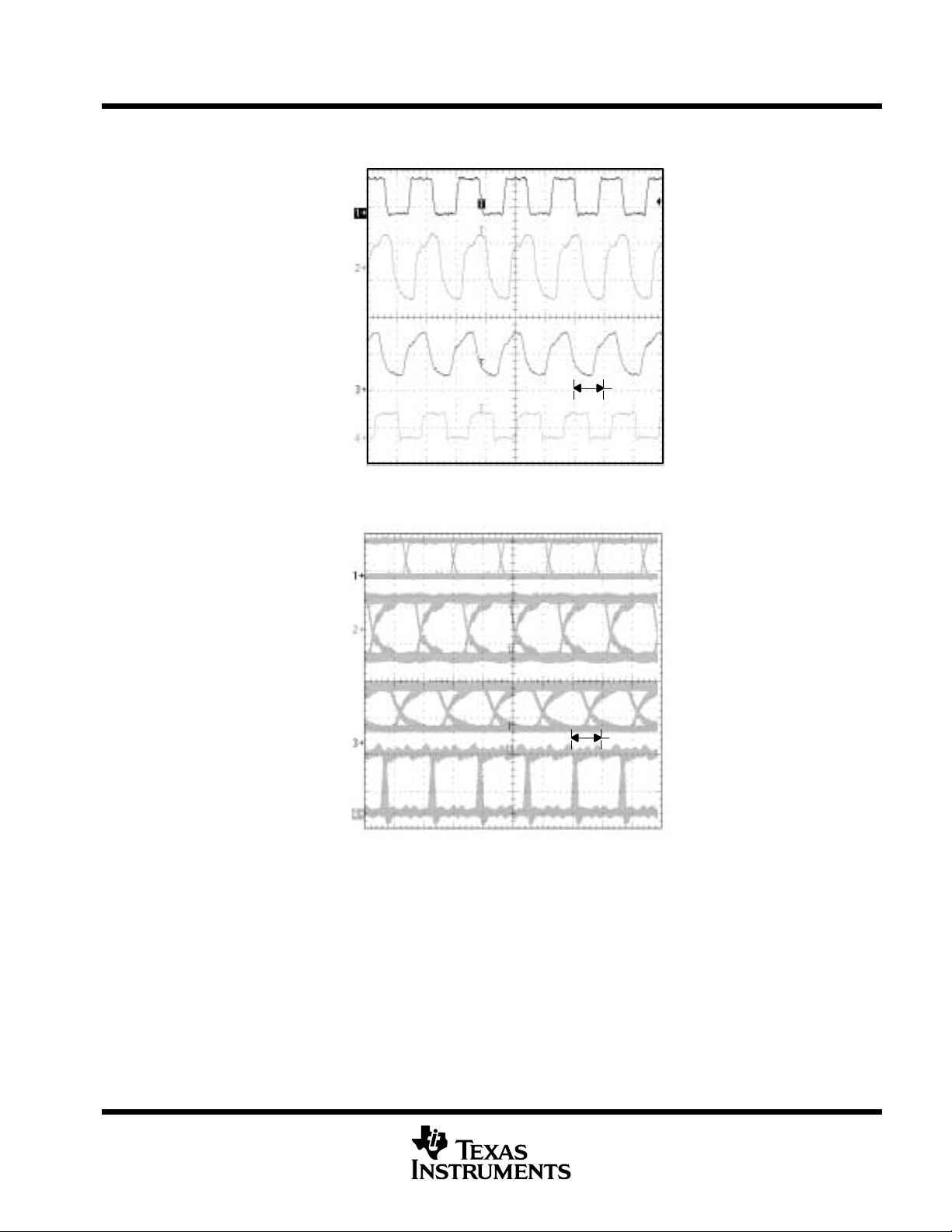
TYPICAL CHARACTERISTICS
Driver Input
(5 V/div)
Driver Output
(2 V/div)
Receiver Input
(2 V/div)
25 ns
Receiver Output
(5 V/div)
Figure 20. Signal Waveforms at 30 Mbps
Driver Input
(5 V/div)
Driver Output
(2 V/div)
Receiver Input
(2 V/div)
12.5 ns
Receiver Output
(5 V/div)
Figure 21. Eye Patterns, Pseudorandom Data at 30 Mbps
12
POST OFFICE BOX 655303 • DALLAS, TEXAS 75265
SN65LBC171, SN75LBC171
TRIPLE DIFFERENTIAL TRANSCEIVERS
SLLS460A – NOVEMBER 2000 – REVISED FEBRUARY 2001
TYPICAL CHARACTERISTICS
Driver Input
(5 V/div)
Driver Output
(2 V/div)
Receiver Input
(2 V/div)
25 ns
Receiver Output
(5 V/div)
Figure 22. Signal Waveforms at 50 Mbps
Driver Input
(5 V/div)
Driver Output
(2 V/div)
Receiver Input
(2 V/div)
12.5 ns
Receiver Output
(5 V/div)
Figure 23. Eye Patterns, Pseudorandom Data at 50 Mbps
POST OFFICE BOX 655303 • DALLAS, TEXAS 75265
13

SN65LBC171, SN75LBC171
TRIPLE DIFFERENTIAL TRANSCEIVERS
SLLS460A – NOVEMBER 2000 – REVISED FEBRUARY 2001
MECHANICAL DATA
DB (R-PDSO-G**) PLASTIC SMALL-OUTLINE
28 PINS SHOWN
0,65
28
1
2,00 MAX
0,38
0,22
15
14
A
0,05 MIN
0,15
5,60
5,00
M
8,20
7,40
Seating Plane
0,10
0,15 NOM
Gage Plane
0°–8°
0,25
0,95
0,55
PINS **
DIM
A MAX
A MIN
NOTES: A. All linear dimensions are in millimeters.
B. This drawing is subject to change without notice.
C. Body dimensions do not include mold flash or protrusion not to exceed 0,15.
D. Falls within JEDEC MO-150
14
6,50
6,50
5,905,90
2016
7,50
6,90
24
8,50
28
10,50
9,907,90
30
10,50
9,90
38
12,90
12,30
4040065 /D 09/00
14
POST OFFICE BOX 655303 • DALLAS, TEXAS 75265

SN65LBC171, SN75LBC171
TRIPLE DIFFERENTIAL TRANSCEIVERS
SLLS460A – NOVEMBER 2000 – REVISED FEBRUARY 2001
MECHANICAL DATA
DW (R-PDSO-G**) PLASTIC SMALL-OUTLINE PACKAGE
16 PINS SHOWN
0.050 (1,27)
16
1
0.020 (0,51)
0.014 (0,35)
9
0.299 (7,59)
0.291 (7,39)
8
A
0.010 (0,25)
0.419 (10,65)
0.400 (10,15)
M
0.010 (0,25) NOM
0°–8°
Gage Plane
0.010 (0,25)
0.050 (1,27)
0.016 (0,40)
0.104 (2,65) MAX
NOTES: A. All linear dimensions are in inches (millimeters).
B. This drawing is subject to change without notice.
C. Body dimensions do not include mold flash or protrusion not to exceed 0.006 (0,15).
D. Falls within JEDEC MS-013
0.012 (0,30)
0.004 (0,10)
DIM
A MAX
A MIN
PINS **
16
0.410
(10,41)
0.400
(10,16)
Seating Plane
0.004 (0,10)
20
0.510
(12,95)
0.500
(12,70)
24
0.610
(15,49)
0.600
(15,24)
28
0.710
(18,03)
0.700
(17,78)
4040000/D 01/00
POST OFFICE BOX 655303 • DALLAS, TEXAS 75265
15

PACKAGE OPTION ADDENDUM
www.ti.com
20-Mar-2007
PACKAGING INFORMATION
Orderable Device Status
(1)
Package
Type
Package
Drawing
Pins Package
Qty
Eco Plan
SN65LBC171DB ACTIVE SSOP DB 20 70 Green (RoHS &
no Sb/Br)
SN65LBC171DBG4 ACTIVE SSOP DB 20 70 Green (RoHS &
no Sb/Br)
SN65LBC171DBR ACTIVE SSOP DB 20 2000 Green (RoHS &
no Sb/Br)
SN65LBC171DBRG4 ACTIVE SSOP DB 20 2000 Green (RoHS &
no Sb/Br)
SN65LBC171DW ACTIVE SOIC DW 20 25 Green (RoHS &
no Sb/Br)
SN65LBC171DWG4 ACTIVE SOIC DW 20 25 Green (RoHS &
no Sb/Br)
SN65LBC171DWR ACTIVE SOIC DW 20 2000 Green(RoHS &
no Sb/Br)
SN65LBC171DWRG4 ACTIVE SOIC DW 20 2000 Green (RoHS &
no Sb/Br)
SN75LBC171DB ACTIVE SSOP DB 20 70 Green (RoHS &
no Sb/Br)
SN75LBC171DBG4 ACTIVE SSOP DB 20 70 Green (RoHS &
no Sb/Br)
SN75LBC171DBR ACTIVE SSOP DB 20 2500 Green (RoHS &
no Sb/Br)
SN75LBC171DBRG4 ACTIVE SSOP DB 20 2500 Green (RoHS &
no Sb/Br)
SN75LBC171DW ACTIVE SOIC DW 20 25 Green (RoHS &
no Sb/Br)
SN75LBC171DWG4 ACTIVE SOIC DW 20 25 Green (RoHS &
no Sb/Br)
SN75LBC171DWR ACTIVE SOIC DW 20 2500 Green (RoHS &
no Sb/Br)
SN75LBC171DWRG4 ACTIVE SOIC DW 20 2500 Green (RoHS &
no Sb/Br)
(1)
The marketing status values are defined as follows:
ACTIVE: Product device recommended for new designs.
LIFEBUY: TI has announced that the device will be discontinued, and a lifetime-buy period is in effect.
NRND: Not recommended for new designs. Device is in production to support existing customers, but TI does not recommend using this part in
a new design.
PREVIEW: Device has been announced but is not in production. Samples may or may not be available.
OBSOLETE: TI has discontinued the production of the device.
(2)
Lead/Ball Finish MSL Peak Temp
CU NIPDAU Level-1-260C-UNLIM
CU NIPDAU Level-1-260C-UNLIM
CU NIPDAU Level-1-260C-UNLIM
CU NIPDAU Level-1-260C-UNLIM
CU NIPDAU Level-1-260C-UNLIM
CU NIPDAU Level-1-260C-UNLIM
CU NIPDAU Level-1-260C-UNLIM
CU NIPDAU Level-1-260C-UNLIM
CU NIPDAU Level-1-260C-UNLIM
CU NIPDAU Level-1-260C-UNLIM
CU NIPDAU Level-1-260C-UNLIM
CU NIPDAU Level-1-260C-UNLIM
CU NIPDAU Level-1-260C-UNLIM
CU NIPDAU Level-1-260C-UNLIM
CU NIPDAU Level-1-260C-UNLIM
CU NIPDAU Level-1-260C-UNLIM
(3)
(2)
Eco Plan - The planned eco-friendly classification: Pb-Free (RoHS), Pb-Free (RoHS Exempt), or Green (RoHS & no Sb/Br) - please check
http://www.ti.com/productcontent for the latest availability information and additional product content details.
TBD: The Pb-Free/Green conversion plan has not been defined.
Pb-Free (RoHS): TI's terms "Lead-Free" or "Pb-Free" mean semiconductor products that are compatible with the current RoHS requirements
for all 6 substances, including the requirement that lead not exceed 0.1% by weight in homogeneous materials. Where designed to be soldered
at high temperatures, TI Pb-Free products are suitable for use in specified lead-free processes.
Pb-Free (RoHS Exempt): This component has a RoHS exemption for either 1) lead-based flip-chip solder bumps used between the die and
package, or 2) lead-based die adhesive used between the die and leadframe. The component is otherwise considered Pb-Free (RoHS
compatible) as defined above.
Green (RoHS & no Sb/Br): TI defines "Green" to mean Pb-Free (RoHS compatible), and free of Bromine (Br) and Antimony (Sb) based flame
retardants (Br or Sb do not exceed 0.1% by weight in homogeneous material)
Addendum-Page 1

PACKAGE OPTION ADDENDUM
www.ti.com
(3)
MSL, Peak Temp. -- The Moisture Sensitivity Level rating according to the JEDEC industry standard classifications, and peak solder
temperature.
Important Information and Disclaimer:The information provided on this page represents TI's knowledge and belief as of the date that it is
provided. TI bases its knowledge and belief on information provided by third parties, and makes no representation or warranty as to the
accuracy of such information. Efforts are underway to better integrate information from third parties. TI has taken and continues to take
reasonable steps to provide representative and accurate information but may not have conducted destructive testing or chemical analysis on
incoming materials and chemicals. TI and TI suppliers consider certain information to be proprietary, and thus CAS numbers and other limited
information may not be available for release.
In no event shall TI's liability arising out of such information exceed the total purchase price of the TI part(s) at issue in this document sold by TI
to Customer on an annual basis.
20-Mar-2007
Addendum-Page 2

PACKAGE MATERIALS INFORMATION
www.ti.com
TAPE AND REEL INFORMATION
11-Mar-2008
*All dimensions are nominal
Device Package
SN65LBC171DBR SSOP DB 20 2000 330.0 16.4 8.2 7.5 2.5 12.0 16.0 Q1
SN65LBC171DWR SOIC DW 20 2000 330.0 24.4 10.8 13.0 2.7 12.0 24.0 Q1
SN75LBC171DWR SOIC DW 20 2500 330.0 24.4 10.8 13.0 2.7 12.0 24.0 Q1
Type
Package
Drawing
Pins SPQ Reel
Diameter
(mm)
Reel
Width
W1 (mm)
A0 (mm) B0 (mm) K0 (mm) P1
(mm)W(mm)
Pin1
Quadrant
Pack Materials-Page 1
PACKAGE MATERIALS INFORMATION
www.ti.com
11-Mar-2008
*All dimensions are nominal
Device Package Type Package Drawing Pins SPQ Length (mm) Width (mm) Height (mm)
SN65LBC171DBR SSOP DB 20 2000 346.0 346.0 33.0
SN65LBC171DWR SOIC DW 20 2000 346.0 346.0 41.0
SN75LBC171DWR SOIC DW 20 2500 346.0 346.0 41.0
Pack Materials-Page 2

IMPORTANT NOTICE
Texas Instruments Incorporated and its subsidiaries (TI) reserve the right to make corrections, modifications, enhancements, improvements,
and other changes to its products and services at any time and to discontinue any product or service without notice. Customers should
obtain the latest relevant information before placing orders and should verify that such information is current and complete. All products are
sold subject to TI’s terms and conditions of sale supplied at the time of order acknowledgment.
TI warrants performance of its hardware products to the specifications applicable at the time of sale in accordance with TI’s standard
warranty. Testing and other quality control techniques are used to the extent TI deems necessary to support this warranty. Except where
mandated by government requirements, testing of all parameters of each product is not necessarily performed.
TI assumes no liability for applications assistance or customer product design. Customers are responsible for their products and
applications using TI components. To minimize the risks associated with customer products and applications, customers should provide
adequate design and operating safeguards.
TI does not warrant or represent that any license, either express or implied, is granted under any TI patent right, copyright, mask work right,
or other TI intellectual property right relating to any combination, machine, or process in which TI products or services are used. Information
published by TI regarding third-party products or services does not constitute a license from TI to use such products or services or a
warranty or endorsement thereof. Use of such information may require a license from a third party under the patents or other intellectual
property of the third party, or a license from TI under the patents or other intellectual property of TI.
Reproduction of TI information in TI data books or data sheets is permissible only if reproduction is without alteration and is accompanied
by all associated warranties, conditions, limitations, and notices. Reproduction of this information with alteration is an unfair and deceptive
business practice. TI is not responsible or liable for such altered documentation. Information of third parties may be subject to additional
restrictions.
Resale of TI products or services with statements different from or beyond the parameters stated by TI for that product or service voids all
express and any implied warranties for the associated TI product or service and is an unfair and deceptive business practice. TI is not
responsible or liable for any such statements.
TI products are not authorized for use in safety-critical applications (such as life support) where a failure of the TI product would reasonably
be expected to cause severe personal injury or death, unless officers of the parties have executed an agreement specifically governing
such use. Buyers represent that they have all necessary expertise in the safety and regulatory ramifications of their applications, and
acknowledge and agree that they are solely responsible for all legal, regulatory and safety-related requirements concerning their products
and any use of TI products in such safety-critical applications, notwithstanding any applications-related information or support that may be
provided by TI. Further, Buyers must fully indemnify TI and its representatives against any damages arising out of the use of TI products in
such safety-critical applications.
TI products are neither designed nor intended for use in military/aerospace applications or environments unless the TI products are
specifically designated by TI as military-grade or "enhanced plastic." Only products designated by TI as military-grade meet military
specifications. Buyers acknowledge and agree that any such use of TI products which TI has not designated as military-grade is solely at
the Buyer's risk, and that they are solely responsible for compliance with all legal and regulatory requirements in connection with such use.
TI products are neither designed nor intended for use in automotive applications or environments unless the specific TI products are
designated by TI as compliant with ISO/TS 16949 requirements. Buyers acknowledge and agree that, if they use any non-designated
products in automotive applications, TI will not be responsible for any failure to meet such requirements.
Following are URLs where you can obtain information on other Texas Instruments products and application solutions:
Products Applications
Amplifiers amplifier.ti.com Audio www.ti.com/audio
Data Converters dataconverter.ti.com Automotive www.ti.com/automotive
DSP dsp.ti.com Broadband www.ti.com/broadband
Clocks and Timers www.ti.com/clocks Digital Control www.ti.com/digitalcontrol
Interface interface.ti.com Medical www.ti.com/medical
Logic logic.ti.com Military www.ti.com/military
Power Mgmt power.ti.com Optical Networking www.ti.com/opticalnetwork
Microcontrollers microcontroller.ti.com Security www.ti.com/security
RFID www.ti-rfid.com Telephony www.ti.com/telephony
RF/IF and ZigBee® Solutions www.ti.com/lprf Video & Imaging www.ti.com/video
Mailing Address: Texas Instruments, Post Office Box 655303, Dallas, Texas 75265
Copyright © 2008, Texas Instruments Incorporated
Wireless www.ti.com/wireless
 Loading...