

www.ti.com
1
2
3
4
8
7
6
5
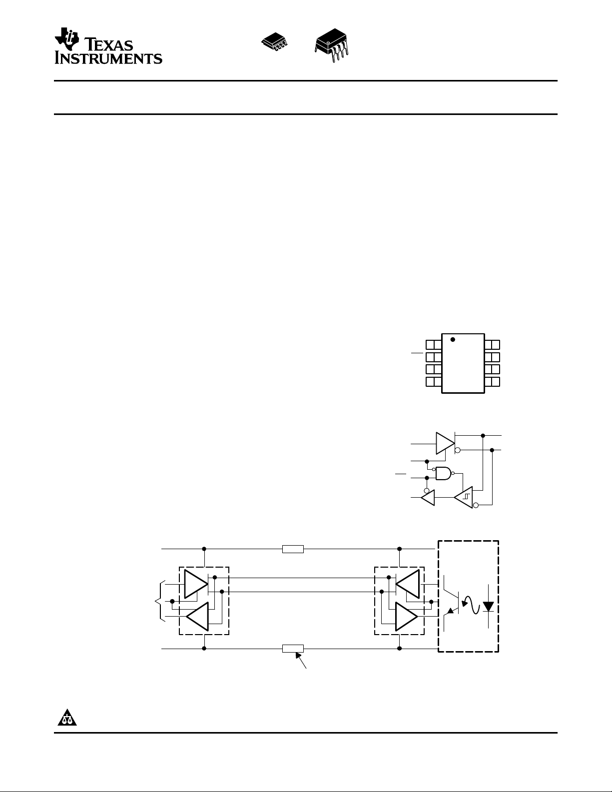
R
RE
DE
D
V
CC
B
A
GND
D or P PACKAGE
(TOP VIEW)
LOGIC DIAGRAM (Positive Logic)
D
A
DE
RE
R
B
Host
SN65HVD08
Power Bus and Return Resistance
Isolation
Barrier
Remote
(One of n Shown)
5 V Power
Direct
Connection
to Host
5 V Return
WIDE SUPPLY RANGE RS-485 TRANSCEIVER
SN75HVD08, SN65HVD08
SLLS550A – NOVEMBER 2002 – REVISED MAY 2003
FEATURES
• Operates With a 3-V to 5.5-V Supply
• Consumes Less Than 90 mW Quiescent
Power
• Open-Circuit, Short Circuit, and Idle-Bus
Failsafe Receiver
• 1/8
th
Unit-Load (up to 256 nodes on the bus)
• Bus-Pin ESD Protection Exceeds 16 kV HBM
• Driver Output Voltage Slew-Rate Limited for
Optimum Signal Quality at 10 Mbps
• Electrically Compatible With ANSI TIA/EIA-485
Standard
APPLICATIONS
• Data Transmission With Remote Stations
Powered From the Host
• Isolated Multipoint Data Buses
• Industrial Process Control Networks
• Point-of-Sale Networks
• Electric Utility Metering
DESCRIPTION
The SN65HVD08 combines a 3-state differential line
driver and differential line receiver designed for balanced data transmission and interoperation with ANSI
TIA/EIA-485-A and ISO-8482E standard-compliant
devices.
The wide supply voltage range and low quiescent
current requirements allow the SN65HVD08s to
operate from a 5-V power bus in the cable with as
much as a 2-V line voltage drop. Busing power in the
cable can alleviate the need for isolated power to be
generated at each connection of a ground-isolated
bus.
The driver differential outputs and receiver differential
inputs connect internally to form a differential input/output (I/O) bus port that is designed to offer
minimum loading to the bus whenever the driver is
disabled or not powered. The drivers and receivers
have active-high and active-low enables respectively,
which can be externally connected together to function as a direction control.
PRODUCTION DATA information is current as of publication date.
Products conform to specifications per the terms of the Texas
Instruments standard warranty. Production processing does not
necessarily include testing of all parameters.
Please be aware that an important notice concerning availability, standard warranty, and use in critical applications of Texas
Instruments semiconductor products and disclaimers thereto appears at the end of this data sheet.
Copyright © 2002–2003, Texas Instruments Incorporated
www.ti.com
SN75HVD08, SN65HVD08
SLLS550A – NOVEMBER 2002 – REVISED MAY 2003
These devices have limited built-in ESD protection. The leads should be shorted together or the device placed in conductive foam
during storage or handling to prevent electrostatic damage to the MOS gates.
ORDERING INFORMATION
PART NUMBER PACKAGE PACKAGE MARKING
SN65HVD08D –40°C to 85°C SOIC VP08
SN65HVD08P –40°C to 85°C PDIP 65HVD08
SN75HVD08D 0°C to 70°C SOIC VN08
SN75HVD08P 0°C to 70°C PDIP 75HVD08
PACKAGE DISSIPATION RATINGS
PACKAGE TA≤ 25°C POWER RATING DERATING FACTOR ABOVE TA= 25°C TA= 85°C POWER RATING
SOIC (D) 710 mW 5.7 mW/°C 369 mW
PDIP (P) 1000 mW 8 mW/°C 520 mW
SPECIFIED TEMPERATURE
RANGE
ABSOLUTE MAXIMUM RATINGS
over operating free-air temperature range unless otherwise noted
Supply voltage, V
Voltage range at A or B -9 V to 14 V
Input voltage range at D, DE, R or RE -0.5 V to V
Voltage input range, transient pulse, A and B, through 100 Ω -25 V to 25 V
Electrostatic discharge All pins 4 kV
Continuous total power dissipation See Dissipation Rating Table
Storage temperature, T
(1) Stresses beyond those listed under "absolute maximum ratings” may cause permanent damage to the device. These are stress ratings
only, and functional operation of the device at these or any other conditions beyond those indicated under "recommended operating
conditions” is not implied. Exposure to absolute-maximum-rated conditions for extended periods may affect device reliability.
(2) All voltage values, except differential I/O bus voltages, are with respect to network ground terminal.
(3) Tested in accordance with JEDEC Standard 22, Test Method A114-A.
(4) Tested in accordance with JEDEC Standard 22, Test Method C101.
CC
Human Body Model
Charged-Device Model
stg
(3)
(4)
(1) (2)
UNIT
-0.3 V to 6 V
CC
A, B, and GND 16 kV
All pins 1 kV
-65°C to 150°C
RECOMMENDED OPERATING CONDITIONS
MIN NOM MAX UNIT
Supply voltage, V
Input voltage at any bus terminal (separately or common mode), V
High-level input voltage, V
Low-level input voltage, V
Differential input voltage, V
High-level output current, I
Low-level output current, I
Operating free-air temperature, T
CC
IH
IL
ID
Driver, driver enable, and receiver enable inputs V
(1)
I
Driver –60
OH
Receiver –8
Driver 60
OL
Receiver 8
SN75HVD08 0 70
A
SN65HVD08 –40 85
(1) The algebraic convention, in which the least positive (most negative) limit is designated as minimum is used in this data sheet.
3 5.5 V
–7 12 V
2.25 V
0 0.8
–12 12
+ 0.5 V
CC
mA
mA
°C
2
www.ti.com
SN75HVD08, SN65HVD08
SLLS550A – NOVEMBER 2002 – REVISED MAY 2003
ELECTRICAL CHARACTERISTICS
over recommended operating conditions unless otherwise noted
PARAMETER TEST CONDITIONS MIN TYP MAX UNIT
|V
| Driver differential output voltage magnitude 1.5 V
OD
∆|V
OD
V
OC(PP)
V
IT+
V
IT-
V
hys
V
OH
V
OL
I
IH
I
IL
I
OS
I
I
I
CC
Change in magnitude of driver differential
| RL= 54 Ω –0.2 0.2 V
output voltage
Peak-to-peak driver common-mode output Center of two 27-Ω load
voltage resistors, See Figure 2
Positive-going receiver differential input volt-
age threshold
Negative-going receiver differential input volt-
age threshold
Receiver differential input voltage threshold
hysteresis(V
- V
)
IT+
IT-
Receiver high-level output voltage IOH= -8 mA 2.4 V
Receiver low-level output voltage IOL= 8 mA 0.4 V
Driver input, driver enable, and receiver en-
able high-level input current
Driver input, driver enable, and receiver en-
able low-level input current
Driver short-circuit output current 7 V < VO< 12 V –265 265 mA
Bus input current (disabled driver) µA
Supply current
RL= 60 Ω, 375 Ω on each output to
-7 V to 12 V, See Figure 1
0.5 V
–200 mV
35 mV
–100 100 µA
–100 100 µA
VI= 12 V 130
VI= -7 V –100
VI= 12 V, V
VI= -7 V. V
= 0 V 130
CC
= 0 V –100
CC
Receiver enabled, driver
disabled, no load
Driver enabled, receiver
disabled, no load
Both disabled 5 µA
Both enabled, no load 16 mA
CC
–10 mV
10
16
V
mA
DRIVER SWITCHING CHARACTERISTICS
over recommended operating conditions unless otherwise noted
PARAMETER TEST CONDITIONS MIN TYP MAX UNIT
t
PHL
t
PLH
t
r
t
f
t
SK(P)
t
en
t
dis
Driver high-to-low propagation delay time 18 40
Driver low-to-high propagation delay time 18 40
Driver 10%-to-90% differential output rise time RL= 54 Ω, CL= 50 pF,See Figure 3 10 55 ns
Driver 90%-to-10% differential output fall time 10 55
Driver differential output pulse skew, |t
Driver enable time
- t
PHL
| 2.5
PLH
Receiver enabled, See Figures 4 and 5 55 ns
Receiver disabled, See Figures 4 and 5 6 µs
Driver disable time Receiver enabled, See Figures 4 and 5 90 ns
3
www.ti.com
60 Ω ±1%
V
OD
0 or 3 V
_
+
–7 V < V
(test)
< 12 V
DE
V
CC
A
B
D
375 Ω ±1%
375 Ω ±1%
V
OC
27 Ω ± 1%
Input
A
B
V
A
V
B
V
OC(PP)
∆V
OC(SS)
V
OC
27 Ω ± 1%
CL = 50 pF ±20%
D
A
B
DE
V
CC
Input: PRR = 500 kHz, 50% Duty Cycle,tr<6ns, tf<6ns, ZO = 50 Ω
CL Includes Fixture and
Instrumentation Capacitance
V
OD
RL = 54 Ω
± 1%
50 Ω
Generator: PRR = 500 kHz, 50% Duty Cycle, tr <6 ns, tf <6 ns, Zo = 50 Ω
t
PLH
t
PHL
1.5 V 1.5 V
3 V
≈ 2 V
≈ –2 V
90%
10%
0 V
V
I
V
OD
t
r
t
f
CL = 50 pF ±20%
CL Includes Fixture
and Instrumentation
Capacitance
D
A
B
DE
V
CC
V
I
Input
Generator
90%
0 V
10%
SN75HVD08, SN65HVD08
SLLS550A – NOVEMBER 2002 – REVISED MAY 2003
RECEIVER SWITCHING CHARACTERISTICS
over recommended operating conditions unless otherwise noted
PARAMETER TEST CONDITIONS MIN TYP MAX UNIT
t
PHL
t
PLH
t
r
t
f
t
SK(P)
t
en
t
dis
Receiver high-to-low propagation delay time 70
Receiver low-to-high propagation delay time 70
Receiver 10%-to-90% differential output rise time CL= 15 pF, See Figure 6 5 ns
Receiver 90%-to-10% differential output fall time 5
Receiver differential output pulse skew, |t
Receiver enable time
- t
PHL
| 4.5
PLH
Driver enabled, See Figure 7 15 ns
Driver disabled, See Figure 8 6 µs
Receiver disable time Driver enabled, See Figure 7 20 ns
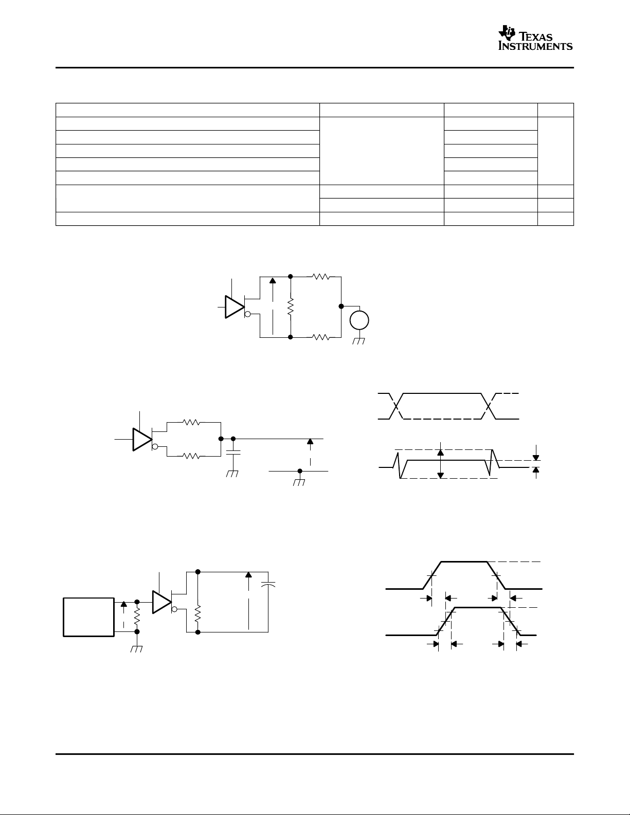
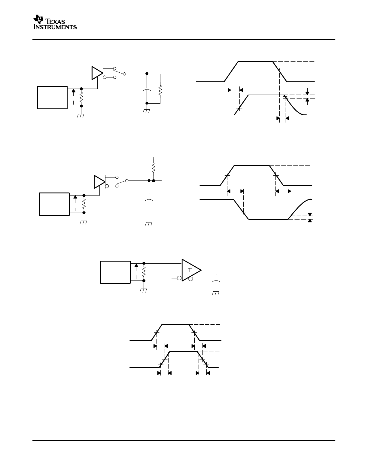
PARAMETER MEASUREMENT INFORMATION
Figure 1. Driver V
With Common-Mode Loading Test Circuit
OD
Figure 2. Test Circuit and Definitions for the Driver Common-Mode Output Voltage
Figure 3. Driver Switching Test Circuit and Voltage Waveforms
4
www.ti.com
RL = 110 Ω
± 1%
Input
Generator
50 Ω
Generator: PRR = 500 kHz, 50% Duty Cycle, tr <6 ns, tf <6 ns, Zo = 50 Ω
3 V
S1
0.5 V
3 V
0 V
V
OH
≈ 0 V
t
PHZ
t
PZH
1.5 V 1.5 V
V
I
V
O
CL = 50 pF ±20%
CL Includes Fixture
and Instrumentation
Capacitance
D
A
B
DE
V
O
V
I
2.3 V
Input
Generator
50 Ω
3 V
V
O
S1
3 V
1.5 V 1.5 V
t
PZL
t
PLZ
2.3 V
0.5 V
≈ 3 V
0 V
V
OL
V
I
V
O
Generator: PRR = 500 kHz, 50% Duty Cycle, tr <6 ns, tf <6 ns, Zo = 50 Ω
RL = 110 Ω
± 1%
CL = 50 pF ±20%
CL Includes Fixture
and Instrumentation
Capacitance
D
A
B
DE
V
I
≈ 3 V
Input
Generator
50 Ω
Generator: PRR = 500 kHz, 50% Duty Cycle, tr <6 ns, tf <6 ns, Zo = 50 Ω
V
O
1.5 V
0 V
1.5 V 1.5 V
3 V
V
OH
V
OL
1.5 V
10%
1.5 V
t
PLH
t
PHL
t
r
t
f
90%
V
I
V
O
CL = 15 pF ±20%
CL Includes Fixture
and Instrumentation
Capacitance
A
B
RE
V
I
R
0 V
90%
10%
Parameter Measurement Information (continued)
Figure 4. Driver High-Level Enable and Disable Time Test Circuit and Voltage Waveforms
SN75HVD08, SN65HVD08
SLLS550A – NOVEMBER 2002 – REVISED MAY 2003
Figure 5. Driver Low-Level Output Enable and Disable Time Test Circuit and Voltage Waveforms
Figure 6. Receiver Switching Test Circuit and Voltage Waveforms
5

www.ti.com
50 Ω
Generator: PRR = 500 kHz, 50% Duty Cycle, tr <6 ns, tf <6 ns, Zo = 50 Ω
V
O
RE
R
A
B
3 V
0 V or 3 V
V
CC
1.5 V 1.5 V
t
PZH
t
PHZ
1.5 V
VOH –0.5 V
3 V
0 V
V
OH
≈ 0 V
V
O
CL = 15 pF ±20%
CL Includes Fixture
and Instrumentation
Capacitance
V
I
DE
D
1 kΩ ± 1%
V
I
A
B
S1
D at 3 V
S1 to B
t
PZL
t
PLZ
1.5 V
VOL +0.5 V
≈ V
CC
V
OL
V
O
D at 0 V
S1 to A
Input
Generator
SN75HVD08, SN65HVD08
SLLS550A – NOVEMBER 2002 – REVISED MAY 2003
Parameter Measurement Information (continued)
Figure 7. Receiver Enable and Disable Time Test Circuit and Voltage Waveforms With Drivers Enabled
6

www.ti.com
Input
Generator 50 Ω
Generator: PRR = 100 kHz, 50% Duty Cycle, tr <6 ns, tf <6 ns, Zo = 50 Ω
V
O
RE
R
A
B
V
CC
1.5 V
t
PZH
1.5 V
3 V
0 V
V
OH
GND
V
I
V
O
0 V or 1.5 V
1.5 V or 0 V CL = 15 pF ±20%
CL Includes Fixture
and Instrumentation
Capacitance
V
I
1 kΩ ± 1%
A
B
S1
A at 1.5 V
B at 0 V
S1 to B
t
PZL
1.5 V
V
OL
V
O
A at 0 V
B at 1.5 V
S1 to A
≈ V
CC
Parameter Measurement Information (continued)
SN75HVD08, SN65HVD08
SLLS550A – NOVEMBER 2002 – REVISED MAY 2003
Figure 8. Receiver Enable Time From Standby (Driver Disabled)
INPUT ENABLE OUTPUTS
DIFFERENTIAL INPUTS ENABLE
VID= VA- V
VID≤ -0.2 V L L
-0.2 V < VID< -0.01 V L ?
-0.01 V ≤ V
X H Z
Open Circuit L H
Short Circuit L H
(1) H = high level; L = low level; Z = high impedance; X = irrelevant;
? = indeterminate
DEVICE INFORMATION
Function Tables
DRIVER
D DE A B
H H H L
L H L H
X L Z Z
Open H H L
RECEIVER
ID
B
RE R
L H
(1)
OUTPUT
(1)
7

www.ti.com
9 V
1 kΩ
100 kΩ
Input
V
CC
D and RE Inputs
9 V
1 kΩ
100 kΩ
Input
V
CC
DE Input
16 V
16 V
100 kΩ
Input
A Input
16 V
16 V
100 kΩ
Input
B Input
16 V
16 V
V
CC
A and B Outputs
9 V
V
CC
R Output
5 Ω
Output
V
CC
V
CC
Output
180 kΩ
36 kΩ
36 kΩ
180 kΩ
36 kΩ
36 kΩ
SN75HVD08, SN65HVD08
SLLS550A – NOVEMBER 2002 – REVISED MAY 2003
EQUIVALENT INPUT AND OUTPUT SCHEMATIC DIAGRAMS
8

www.ti.com
2.5
2
1.5
1
2.5 3 3.5 4 4.5
Differential Output Voltage – V
3
3.5
DIFFERENTIAL OUTPUT VOLT AGE
vs
SUPPLY VOLT AGE
4
5 5.5 6
VCC – Supply Voltage – V
D and DE at V
CC
RL = 54 Ω
TA = –40°C
TA = 25°C
TA = 85°C
0 0.6 1.2 1.8 2.4 3 3.6 4.2 4.8 5.4
0
10
20
30
40
50
60
70
I
O
– Driver Output Current – mA
DRIVER OUTPUT CURRENT
vs
SUPPLY VOLT AGE
VCC – Supply Voltage – V
TA = 25°C
DE at V
CC
D at V
CC
RL = 54 Ω
1
0.5
0
2.5 3.5 4.5
Logic Input Threshold Voltage – V
1.5
2
LOGIC INPUT THRESHOLD VOLTAGE
vs
SUPPLY VOLT AGE
2.5
5.5 6.5
VCC – Supply Voltage – V
Positive Going
Negative Going
TA = 25°C
D, DE or RE input
40
60
80
100
120
0 2.5 5 7.5 10
Signaling Rate – Mbps
RMS SUPPLY CURRENT
vs
SIGNALING RATE
I
CC
– RMS Supply Current – mA
TA = 25°C
RE at V
CC
DE at V
CC
R
L
= 54 Ω
CL = 50 pF
VCC = 5 V
SN75HVD08, SN65HVD08
SLLS550A – NOVEMBER 2002 – REVISED MAY 2003
TYPICAL CHARACTERISTICS
Figure 9. Figure 10.
Figure 11. Figure 12.
9

www.ti.com
+
–
+
–
V
S
R
S
R
S
I
L
R
L
VL = VS – 2RSI
L
DC-to-DC
Converter
Opto
Isolators
DC-to-DC
Converter
Opto
Isolators
Local Power
Source
Rest of
Board
Local Power
Source
Rest of
Board
SN75HVD08, SN65HVD08
SLLS550A – NOVEMBER 2002 – REVISED MAY 2003
APPLICATION INFORMATION
As electrical loads are physically distanced from their
power source, the effects of supply and return line
impedance and the resultant voltage drop must be
accounted. If the supply regulation at the load cannot
be maintained to the circuit requirements, it forces the
use of remote sensing, additional regulation at the
load, bigger or shorter cables, or a combination of
these. The SN65HVD08 eases this problem by relaxing the supply requirements to allow for more
variation in the supply voltage over typical RS-485
transceivers.
SUPPLY SOURCE IMPEDANCE
In the steady state, the voltage drop from the source
to the load is simply the wire resistance times the
load current as modeled in Figure 13 .
Figure 13. Steady-State Circuit Model
For example, if you were to provide 5-V ±5% supply
power to a remote circuit with a maximum load
requirement of 0.1 A (one SN65HVD08), the voltage
at the load would fall below the 4.5-V minimum of
most 5-V circuits with as little as 5.8 m of 28-GA
conductors. Table 1 summarizes wire resistance and
the length for 4.5 V and 3 V at the load with 0.1 A of
load current. The maximum lengths would scale
linearly for higher or lower load currents.
Under dynamic load requirements, the distributed
inductance and capacitance of the power lines may
not be ignored and decoupling capacitance at the
load is required. The amount depends upon the
magnitude and frequency of the load current change
but, if only powering the SN65HVD08, a 0.1 µF
ceramic capacitor is usually sufficient.
OPTO-ISOLATED DATA BUSES
Long RS-485 circuits can create large ground loops
and pick up common-mode noise voltages in excess
of the range tolerated by standard RS-485 circuits. A
common remedy is to provide galvanic isolation of the
data circuit from earth or local grounds.
Transformers, capacitors, or phototransistors most
often provide isolation of the bus and the local node.
Transformers and capacitors require changing signals
to transfer the information over the isolation barrier
and phototransistors (opto-isolators) can pass
steady-state signals. Each of these methods incurs
additional costs and complexity, the former in clock
encoding and decoding of the data stream and the
latter in requiring an isolated power supply.
Quite often, the cost of isolated power is repeated at
each node connected to the bus as shown in Figure 14 . The possibly lower-cost solution is to generate this supply once within the system and then
distribute it along with the data line(s) as shown in
Figure 15 .
Table 1. Maximum Cable Lengths for Minimum
Load Voltages at 0.1 A Load
WIRE RESISTANCE 4.5 V LENGTH 3-v LENGTH
SIZE AT 0.1 A AT 0.1 A
28 Gage 0.213 Ω/m 5.8 m 41.1 m
24 Gage 0.079 Ω/m 15.8 m 110.7 m
22 Gage 0.054 Ω/m 23.1 m 162.0 m
20 Gage 0.034 Ω/m 36.8 m 257.3 m
18 Gage 0.021 Ω/m 59.5 m 416.7 m
10
Figure 14. Isolated Power at Each Node

www.ti.com
SN65HVD08
Local Power
Source
Rest of
Board
Opto
Isolators
Local Power
Source
Rest of
Board
Opto
Isolators
+5 V
–5 V
Bus
+5 V
“1”
+5 V
DE/RE
Data
(I/O)
Side A Side B
Channel 1
Channel 2
D
2A
G
A
V
SB
D
2B
D
1B
G
A
D
1A
V
SA
R/T
1A
R/T
1B
R/T
2B
R/T
2A
D
A
DE
RE
R
B
SN65HVD08
ISO150
Figure 15. Distribution of Isolated Power
SN75HVD08, SN65HVD08
SLLS550A – NOVEMBER 2002 – REVISED MAY 2003
AN OPTO ALTERNATIVE
The ISO150 is a two-channel, galvanically isolated
data coupler capable of data rates of 80 Mbps. Each
channel can be individually programmed to transmit
data in either direction.
Data is transmitted across the isolation barrier by
coupling complementary pulses through high-voltage
0.4-pF capacitors. Receiver circuitry restores the
pulses to standard logic levels. Differential signal
transmission rejects isolation-mode voltage transients
up to 1.6 kV/ms.
ISO150 avoids the problems commonly associated
with opto-couplers. Optically-isolated couplers require
high current pulses and allowance must be made for
LED aging. The ISO150's Bi-CMOS circuitry operates
at 25 mW per channel with supply voltage range
matching that of the SN65HVD08 of 3 V to 5.5 V.
Figure 16 shows a typical circuit.
The features of the SN65HVD08 are particularly good
for the application of Figure 15 . Due to added supply
source impedance, the low quiescent current requirements and wide supply voltage tolerance allow for the
poorer load regulation.
Figure 16. Isolated RS-485 Interface
11

MECHANICAL DATA
MPDI001A – JANUARY 1995 – REVISED JUNE 1999
P (R-PDIP-T8) PLASTIC DUAL-IN-LINE
0.400 (10,60)
0.355 (9,02)
8
5
0.260 (6,60)
0.240 (6,10)
1
0.021 (0,53)
0.015 (0,38)
NOTES: A. All linear dimensions are in inches (millimeters).
B. This drawing is subject to change without notice.
C. Falls within JEDEC MS-001
4
0.070 (1,78) MAX
0.020 (0,51) MIN
0.200 (5,08) MAX
0.125 (3,18) MIN
0.100 (2,54)
0.010 (0,25)
Seating Plane
M
0.325 (8,26)
0.300 (7,62)
0.015 (0,38)
Gage Plane
0.010 (0,25) NOM
0.430 (10,92)
MAX
4040082/D 05/98
For the latest package information, go to http://www.ti.com/sc/docs/package/pkg_info.htm
POST OFFICE BOX 655303 • DALLAS, TEXAS 75265


IMPORTANT NOTICE
Texas Instruments Incorporated and its subsidiaries (TI) reserve the right to make corrections, modifications,
enhancements, improvements, and other changes to its products and services at any time and to discontinue
any product or service without notice. Customers should obtain the latest relevant information before placing
orders and should verify that such information is current and complete. All products are sold subject to TI’s terms
and conditions of sale supplied at the time of order acknowledgment.
TI warrants performance of its hardware products to the specifications applicable at the time of sale in
accordance with TI’s standard warranty. Testing and other quality control techniques are used to the extent TI
deems necessary to support this warranty . Except where mandated by government requirements, testing of all
parameters of each product is not necessarily performed.
TI assumes no liability for applications assistance or customer product design. Customers are responsible for
their products and applications using TI components. To minimize the risks associated with customer products
and applications, customers should provide adequate design and operating safeguards.
TI does not warrant or represent that any license, either express or implied, is granted under any TI patent right,
copyright, mask work right, or other TI intellectual property right relating to any combination, machine, or process
in which TI products or services are used. Information published by TI regarding third-party products or services
does not constitute a license from TI to use such products or services or a warranty or endorsement thereof.
Use of such information may require a license from a third party under the patents or other intellectual property
of the third party, or a license from TI under the patents or other intellectual property of TI.
Reproduction of information in TI data books or data sheets is permissible only if reproduction is without
alteration and is accompanied by all associated warranties, conditions, limitations, and notices. Reproduction
of this information with alteration is an unfair and deceptive business practice. TI is not responsible or liable for
such altered documentation.
Resale of TI products or services with statements different from or beyond the parameters stated by TI for that
product or service voids all express and any implied warranties for the associated TI product or service and
is an unfair and deceptive business practice. TI is not responsible or liable for any such statements.
Following are URLs where you can obtain information on other Texas Instruments products and application
solutions:
Products Applications
Amplifiers amplifier.ti.com Audio www.ti.com/audio
Data Converters dataconverter.ti.com Automotive www.ti.com/automotive
DSP dsp.ti.com Broadband www.ti.com/broadband
Interface interface.ti.com Digital Control www.ti.com/digitalcontrol
Logic logic.ti.com Military www.ti.com/military
Power Mgmt power.ti.com Optical Networking www.ti.com/opticalnetwork
Microcontrollers microcontroller.ti.com Security www.ti.com/security
Telephony www.ti.com/telephony
Video & Imaging www.ti.com/video
Wireless www.ti.com/wireless
Mailing Address: Texas Instruments
Post Office Box 655303 Dallas, Texas 75265
Copyright 2004, Texas Instruments Incorporated
 Loading...