

www.ti.com
1
2
3
4
8
7
6
5
R
RE
DE
D
V
CC
B
A
GND
D OR P PACKAGE
(TOP VIEW)
1
2
3
4
6
7
A
B
R
RE
DE
D
LOGIC DIAGRAM
(POSITIVE LOGIC)
0
0.5
1
1.5
2
2.5
3
3.5
4
4.5
5
0 20 40 60 80 100 120
- Differential Output Voltage - V
DIFFERENTIAL OUTPUT VOLTAGE
vs
DIFFERENTIAL OUTPUT CURRENT
V
O
IOD - Differential Output Current - mA
60 Ω Load
Line
30 Ω Load
Line
TA = 25°C
DE at V
CC
D at V
CC
V
CC
= 5 V
查询SN65HVD07DG4供应商
HIGH OUTPUT RS-485 TRANSCEIVERS
FEATURES DESCRIPTION
• Minimum Differential Output Voltage of 2.5 V
Into a 54- Ω Load
• Open-Circuit, Short-Circuit, and Idle-Bus
Failsafe Receiver
• 1/8
• Bus-Pin ESD Protection Exceeds 16 kV HBM
• Driver Output Slew Rate Control Options
• Electrically Compatible With ANSI
• Low-Current Standby Mode . . . 1 µA Typical
• Glitch-Free Power-Up and Power-Down
• Pin Compatible With Industry Standard
APPLICATIONS
• Data Transmission Over Long or Lossy Lines
• Profibus Line Interface
• Industrial Process Control Networks
• Point-of-Sale (POS) Networks
• Electric Utility Metering
• Building Automation
• Digital Motor Control
th
Unit-Load Option Available (Up to 256
Nodes on the Bus)
TIA/EIA-485-A Standard
Protection for Hot-Plugging Applications
SN75176
or Electrically Noisy Environments
SN65HVD05 , , SN65HVD06
SN75HVD05 , SN65HVD07
SN75HVD06 , SN75HVD07
SLLS533D – MAY 2002 – REVISED JULY 2006
The SN65HVD05, SN75HVD05, SN65HVD06,
SN75HVD06, SN65HVD07, and SN75HVD07
combine a 3-state differential line driver and
differential line receiver. They are designed for
balanced data transmission and interoperate with
ANSI TIA/EIA-485-A and ISO 8482E
standard-compliant devices. The driver is designed
to provide a differential output voltage greater than
that required by these standards for increased noise
margin. The drivers and receivers have active-high
and active-low enables respectively, which can be
externally connected together to function as direction
control.
The driver differential outputs and receiver
differential inputs connect internally to form a
differential input/ output (I/O) bus port that is
designed to offer minimum loading to the bus
whenever the driver is disabled or not powered.
These devices feature wide positive and negative
common-mode voltage ranges, making them suitable
for party-line applications.
PRODUCTION DATA information is current as of publication date.
Products conform to specifications per the terms of the Texas
Instruments standard warranty. Production processing does not
necessarily include testing of all parameters.
Please be aware that an important notice concerning availability, standard warranty, and use in critical applications of Texas
Instruments semiconductor products and disclaimers thereto appears at the end of this data sheet.
Copyright © 2002–2006, Texas Instruments Incorporated
www.ti.com
SN65HVD05 , , SN65HVD06
SN75HVD05 , SN65HVD07
SN75HVD06 , SN75HVD07
SLLS533D – MAY 2002 – REVISED JULY 2006
These devices have limited built-in ESD protection. The leads should be shorted together or the device placed in conductive foam
during storage or handling to prevent electrostatic damage to the MOS gates.
ORDERING INFORMATION
SIGNALING UNIT
RATE LOAD
40 Mbps 1/2 No SN65HVD05D SN65HVD05P 65HVD05 VP05
10 Mbps 1/8 Yes 40°C to 85°C SN65HVD06D SN65HVD06P 65HVD06 VP06
1 Mbps 1/8 Yes SN65HVD07D SN65HVD07P 65HVD07 VP07
40 Mbps 1/2 No SN75HVD05D SN75HVD05P 75HVD05 VN05
10 Mbps 1/8 Yes 0°C to 70°C SN75HVD06D SN75HVD06P 75HVD06 VN06
1 Mbps 1/8 Yes SN75HVD07D SN75HVD07P 75HVD07 VN07
(1) For the most current package and ordering information, see the Package Option Addendum at the end of this document, or see the TI
web site at www.ti.com .
(2) The D package is available taped and reeled. Add an R suffix to the device type (i.e., SN65HVD05DR).
DRIVER
OUTPUT SLOPE T
CONTROL
A
PART NUMBER
(1)
MARKED AS
(2)
PLASTIC SMALL
DUAL-IN-LINE OUTLINE
PACKAGE IC (SOIC)
(PDIP) PACKAGE
PACKAGE DISSIPATION RATINGS
(See Figure 12 and Figure 13 )
PACKAGE
(2)
D
(3)
D
P 1000 mW 8.0 mW/°C 640 mW 520 mW
(1) This is the inverse of the junction-to-ambient thermal resistance when board-mounted and with no air flow.
(2) Tested in accordance with the Low-K thermal metric definitions of EIA/JESD51-3
(3) Tested in accordance with the High-K thermal metric definitions of EIA/JESD51-7
TA≤ 25°C DERATING FACTOR
POWER RATING ABOVE TA= 25°C POWER RATING POWER RATING
710 mW 5.7 mW/°C 455 mW 369 mW
1282 mW 10.3 mW/°C 821 mW 667 mW
(1)
TA= 70°C TA= 85°C
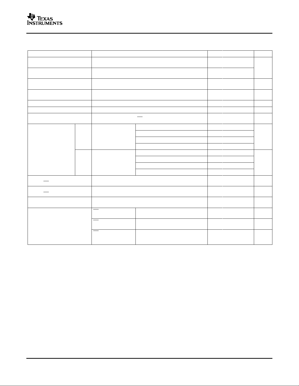
ABSOLUTE MAXIMUM RATINGS
over operating free-air temperature range unless otherwise noted
Supply voltage range, V
Voltage range at A or B -9 V to 14 V
Input voltage range at D, DE, R or RE -0.5 V to V
Voltage input range, transient pulse, A and B, through 100 Ω (see Figure 11 ) -50 V to 50 V
Receiver output current, I
Electrostatic discharge All pins 4 kV
Continuous total power dissipation See Dissipation Rating Table
(1) Stresses beyond those listed under "absolute maximum ratings” may cause permanent damage to the device. These are stress ratings
only, and functional operation of the device at these or any other conditions beyond those indicated under" recommended operating
conditions” is not implied. Exposure to absolute-maximum-rated conditions for extended periods may affect device reliability.
(2) All voltage values, except differential I/O bus voltages, are with respect to network ground terminal.
(3) Tested in accordance with JEDEC Standard 22, Test Method A114-A.
(4) Tested in accordance with JEDEC Standard 22, Test Method C101.
2
CC
O
Human body model
Charged-device model
(3)
(4)
Submit Documentation Feedback
(1) (2)
SN65HVD05, SN65HVD06, SN65HVD07
SN75HVD05, SN75HVD06, SN75HVD07
-0.3 V to 6 V
–11 mA to 11mA
A, B, and GND 16 kV
All pins 1 kV
+ 0.5 V
CC
www.ti.com
SN65HVD05 , , SN65HVD06
SN75HVD05 , SN65HVD07
SN75HVD06 , SN75HVD07
SLLS533D – MAY 2002 – REVISED JULY 2006
RECOMMENDED OPERATING CONDITIONS
MIN NOM MAX UNIT
Supply voltage, V
Voltage at any bus terminal (separately or common mode) VIor V
High-level input voltage, V
Low-level input voltage, V
CC
IC
IH
IL
D, DE, RE 2 V
D, DE, RE 0.8 V
Differential input voltage, VID(see Figure 7 ) -12 12 V
High-level output current, I
Low-level output current, I
OH
OL
Driver -100
Receiver -8
Driver 100
Receiver 8
SN65HVD05
SN65HVD06 -40 85 °C
Operating free-air temperature, T
SN65HVD07
A
SN75HVD05
SN75HVD06 0 70 °C
SN75HVD07
(1) The algebraic convention, in which the least positive (most negative) limit is designated as minimum is used in this data sheet.
4.5 5.5 V
(1)
-7
12 V
mA
mA
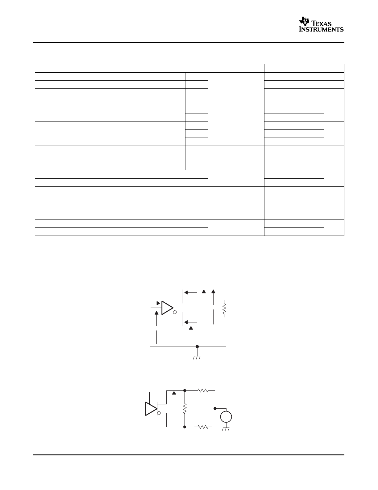
DRIVER ELECTRICAL CHARACTERISTICS
over operating free-air temperature range unless otherwise noted
PARAMETER TEST CONDITIONS MIN TYP
V
IK
Input clamp voltage II= -18 mA -1.5 V
No Load V
|V
| Differential output voltage RL= 54 Ω , See Figure 4 2.5 V
OD
V
= -7 V to 12 V, See Figure 2 2.2
test
∆ |V
OD
V
OC(SS)
∆ V
OC(SS)
Change in magnitude of differential output
| See Figure 4 and Figure 2 -0.2 0.2 V
voltage
Steady-state common-mode output voltage 2.2 3.3 V
Change in steady-state common-mode
output voltage
See Figure 3
-0.1 0.1 V
HVD05 600
V
OC(PP)
Peak-to-peak common-mode
output voltage
HVD06 See Figure 3 500 mV
HVD07 900
I
OZ
I
I
I
OS
C
(diff)
High-impedance output current See receiver input currents
Input current µA
D -100 0
DE 0 100
Short-circuit output current -7 V ≤ VO≤ 12 V -250 250 mA
Differential output capacitance VID= 0.4 sin (4E6 π t) + 0.5 V, DE at 0 V 16 pF
RE at VCC,
D & DE at VCC, 9 15 mA
No load
Receiver disabled
and driver enabled
RE at VCC, Receiver disabled
I
CC
Supply current D at V
No load (standby)
RE at 0 V,
D & DE at VCC, 9 15 mA
No load
DE at 0 V, and driver disabled 1 5 µA
CC
Receiver enabled
and driver enabled
(1) All typical values are at 25°C and with a 5-V supply.
(1)
MAX UNIT
CC
Submit Documentation Feedback
3
www.ti.com
SN65HVD05 , , SN65HVD06
SN75HVD05 , SN65HVD07
SN75HVD06 , SN75HVD07
SLLS533D – MAY 2002 – REVISED JULY 2006
DRIVER SWITCHING CHARACTERISTICS
over operating free-air temperature range unless otherwise noted
PARAMETER TEST CONDITIONS MIN TYP
HVD05 6.5 11
t
PLH
t
PHL
t
r
t
f
t
sk(p)
t
sk(pp)
t
PZH1
t
PHZ
t
PZL1
t
PLZ
t
PZH2
t
PZL2
(1) All typical values are at 25°C and with a 5-V supply.
(2) t
Propagation delay time, low-to-high-level output HVD06 27 40 ns
HVD07 250 400
HVD05 6.5 11
Propagation delay time, high-to-low-level output HVD06 27 40 ns
HVD07 250 400
HVD05 2.7 3.6 6
Differential output signal rise time HVD06 18 28 55 ns
RL= 54 Ω , CL= 50 pF,
See Figure 4
HVD07 150 300 450
HVD05 2.7 3.6 6
Differential output signal fall time HVD06 18 28 55 ns
HVD07 150 300 450
HVD05 2
Pulse skew (|t
- t
PHL
|) HVD06 2.5 ns
PLH
HVD07 10
HVD05 3.5
(2)
Part-to-part skew HVD06 14 ns
HVD07 100
HVD05 25
Propagation delay time,
high-impedance-to-high-level output
Propagation delay time,
high-level-to-high-impedance output
HVD06 45 ns
HVD07 250
HVD05 25
RE at 0 V, RL= 110 Ω ,
See Figure 5
HVD06 60 ns
HVD07 250
HVD05 15
Propagation delay time,
high-impedance-to-low-level output
Propagation delay time,
low-level-to-high-impedance output
HVD06 45 ns
HVD07 200
HVD05 14
RE at 0 V, RL= 110 Ω ,
See Figure 6
HVD06 90 ns
HVD07 550
Propagation delay time, standby-to-high-level output 6 µs
Propagation delay time, standby-to-low-level output 6 µs
is the magnitude of the difference in propagation delay times between any specified terminals of two devices when both devices
sk(pp)
operate with the same supply voltages, at the same temperature, and have identical packages and test circuits.
RL= 110 Ω , RE at 3 V,
See Figure 5
RL= 110 Ω , RE at 3 V,
See Figure 6
(1)
MAX UNIT
4
Submit Documentation Feedback
www.ti.com
RECEIVER ELECTRICAL CHARACTERISTICS
over operating free-air temperature range unless otherwise noted
PARAMETER TEST CONDITIONS MIN TYP
Positive-going input
V
IT+
threshold voltage
Negative-going input
V
IT-
threshold voltage
Hysteresis voltage
V
hys
(V
- V
)
IT+
IT-
Enable-input clamp
V
IK
voltage
V
High-level output voltage VID= 200 mV, IOH= -8 mA, See Figure 7 4 V
OH
V
Low-level output voltage VID= -200 mV, IOL= 8 mA, See Figure 7 0.4 V
OL
High-impedance-state
I
OZ
output current
HVD05 Other inputat 0 V mA
I
Bus input current
I
HVD06
HVD07
High-level input current,
I
IH
RE
Low-level input current,
I
IL
RE
Differential input
C
(diff)
capacitance
I
Supply current D at VCC, No load (standby)
CC
(1) All typical values are at 25°C and with a 5-V supply.
IO= -8 mA 0.01
IO= 8 mA -0.2
II= -18 mA -1.5 V
VO= 0 or V
CC
Other inputat 0 V mA
VIH= 2 V -60 26.4 µA
VIL= 0.8 V -60 27.4 µA
VI= 0.4 sin (4E6 π t) + 0.5 V, DE at 0 V 16 pF
RE at 0 V, D & DE at
0 V, No load
RE at VCC, DE at 0 V, Receiver disabled and driver disabled
RE at 0 V,
D & DE at VCC, Receiver enabled and driver enabled 9 15 mA
No load
SN65HVD05 , , SN65HVD06
SN75HVD05 , SN65HVD07
SN75HVD06 , SN75HVD07
SLLS533D – MAY 2002 – REVISED JULY 2006
(1)
MAX UNIT
35 mV
RE at V
CC
VAor VB= 12 V 0.23 0.5
VAor VB= 12 V, V
= 0 V 0.3 0.5
CC
VAor VB= -7 V -0.4 0.13
VAor VB= -7 V, V
= 0 V -0.4 0.15
CC
VAor VB= 12 V 0.06 0.1
VAor VB= 12 V, V
= 0 V 0.08 0.13
CC
VAor VB= -7 V -0.1 0.05
VAor VB= -7 V, V
= 0 V -0.05 0.03
CC
Receiver enabled and driver disabled 5 10 mA
-1 1 µA
1 5 µA
V
Submit Documentation Feedback
5
www.ti.com
I
OA
V
OD 54 Ω ±1%
0 or 3 V
V
OA
V
OB
I
OB
DE
V
CC
I
I
V
I
A
B
60 Ω ±1%
V
OD
0 or 3 V
_
+ -7 V < V
(test)
< 12 V
DE
V
CC
A
B
D
375 Ω ±1%
375 Ω ±1%
SN65HVD05 , , SN65HVD06
SN75HVD05 , SN65HVD07
SN75HVD06 , SN75HVD07
SLLS533D – MAY 2002 – REVISED JULY 2006
RECEIVER SWITCHING CHARACTERISTICS
over operating free-air temperature range unless otherwise noted
PARAMETER TEST CONDITIONS MIN TYP
t
PLH
t
PHL
t
PLH
t
PHL
t
sk(p)
t
sk(pp)
t
r
t
f
t
PZH1
t
PZL1
t
PHZ
t
PLZ
t
PZH2
t
PZL2
Propagation delay time, low-to-high-level output 1/2 UL HVD05 14.6 25 ns
Propagation delay time, high-to-low-level output 1/2 UL HVD05 14.6 25 ns
Propagation delay time, low-to-high-level output 1/8 UL ns
Propagation delay time, high-to-low-level output 1/8 UL ns
Pulse skew (|t
(2)
Part-to-part skew HVD06 14 ns
- t
PHL
|) HVD06 4.5 ns
PLH
Output signal rise time 2 3
Output signal fall time 2 3
Output enable time to high level 10
Output enable time to low level 10
Output disable time from high level 15
Output disable time from low level 15
Propagation delay time, standby-to-high-level output 6
Propagation delay time, standby-to-low-level output 6
(1)
MAX UNIT
HVD06 55 70
HVD07 55 70
VID= -1.5 V to 1.5 V,
HVD06 CL= 15 pF, 55 70
HVD07 55 70
See Figure 8
HVD05 2
HVD07 4.5
HVD05 6.5
HVD07 14
CL= 15 pF,
See Figure 8
CL= 15 pF,
DE at 3 V, ns
See Figure 9
CL= 15 pF, DE at 0,
See Figure 10
ns
µs
(1) All typical values are at 25°C and with a 5-V supply.
(2) t
is the magnitude of the difference in propagation delay times between any specified terminals of two devices when both devices
sk(pp)
operate with the same supply voltages, at the same temperature, and have identical packages and test circuits.
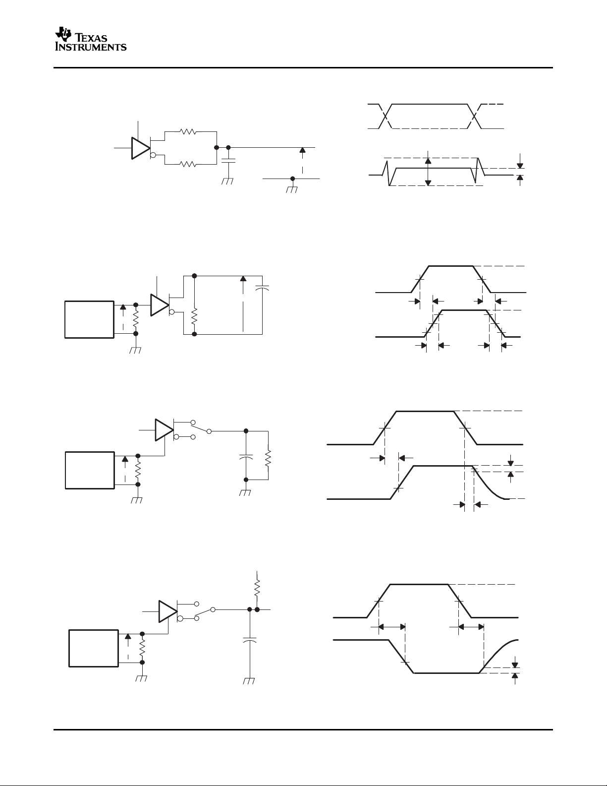
Figure 1. Driver V
6
PARAMETER MEASUREMENT INFORMATION
Figure 2. Driver V
Test Circuit and Voltage and Current Definitions
OD
With Common-Mode Loading Test Circuit
OD
Submit Documentation Feedback
www.ti.com
V
OC
27 Ω ± 1%
Input
A
B
V
A
V
B
V
OC(PP)
∆V
OC(SS)
V
OC
27 Ω ± 1%
CL = 50 pF ±20%
D
A
B
DE
V
CC
Input: PRR = 500 kHz, 50% Duty Cycle,tr<6ns, tf<6ns, ZO = 50 Ω
CL Includes Fixture and
Instrumentation Capacitance
V
OD
RL = 54 Ω
± 1%
50 Ω
Generator: PRR = 500 kHz, 50% Duty Cycle, tr <6 ns, tf <6 ns, Zo = 50 Ω
t
PLH
t
PHL
1.5 V 1.5 V
3 V
≈ 2 V
≈ –2 V
90%
10%
0 V
V
I
V
OD
t
r
t
f
CL = 50 pF ±20%
CL Includes Fixture
and Instrumentation
Capacitance
D
A
B
DE
V
CC
V
I
Input
Generator
90%
0 V
10%
0 V
RL = 110 Ω
± 1%
Input
Generator
50 Ω
Generator: PRR = 100 kHz, 50% Duty Cycle, tr <6 ns, tf <6 ns, Zo = 50 Ω
3 V
S1
0.5 V
3 V
0 V
V
OH
≈ 0 V
t
PHZ
t
PZH(1 & 2)
1.5 V 1.5 V
V
I
V
O
CL = 50 pF ±20%
CL Includes Fixture
and Instrumentation
Capacitance
D
A
B
DE
V
O
V
I
2.3 V
Input
Generator
50 Ω
3 V
V
O
S1
1.5 V 1.5 V
t
PLZ
2.3 V
0.5 V
≈ 3 V
0 V
V
OL
V
I
V
O
Generator: PRR = 100 kHz, 50% Duty Cycle, tr <6 ns, tf <6 ns, Zo = 50 Ω
RL = 110 Ω
± 1%
CL = 50 pF ±20%
CL Includes Fixture
and Instrumentation
Capacitance
D
A
B
DE
V
I
t
PZL(1 & 2)
V
CC
V
CC
SN65HVD05 , , SN65HVD06
SN75HVD05 , SN65HVD07
SN75HVD06 , SN75HVD07
SLLS533D – MAY 2002 – REVISED JULY 2006
PARAMETER MEASUREMENT INFORMATION (continued)
Figure 3. Test Circuit and Definitions for the Driver Common-Mode Output Voltage
Figure 4. Driver Switching Test Circuit and Voltage Waveforms
Figure 5. Driver High-Level Enable and Disable Time Test Circuit and Voltage Waveforms
Submit Documentation Feedback
Figure 6. Driver Low-Level Output Enable and Disable Time Test Circuit and Voltage Waveforms
7
www.ti.com
V
ID
V
A
V
B
I
O
A
B
I
B
V
O
R
I
A
V
IC
VA + V
B
2
Input
Generator
50 Ω
Generator: PRR = 100 kHz, 50% Duty Cycle, tr <6 ns, tf <6 ns, Zo = 50 Ω
V
O
1.5 V
0 V
1.5 V 1.5 V
3 V
V
OH
V
OL
1.5 V
10%
1.5 V
t
PLH
t
PHL
t
r
t
f
90%
V
I
V
O
CL = 15 pF ±20%
CL Includes Fixture
and Instrumentation
Capacitance
A
B
RE
V
I
R
0 V
90%
10%
SN65HVD05 , , SN65HVD06
SN75HVD05 , SN65HVD07
SN75HVD06 , SN75HVD07
SLLS533D – MAY 2002 – REVISED JULY 2006
PARAMETER MEASUREMENT INFORMATION (continued)
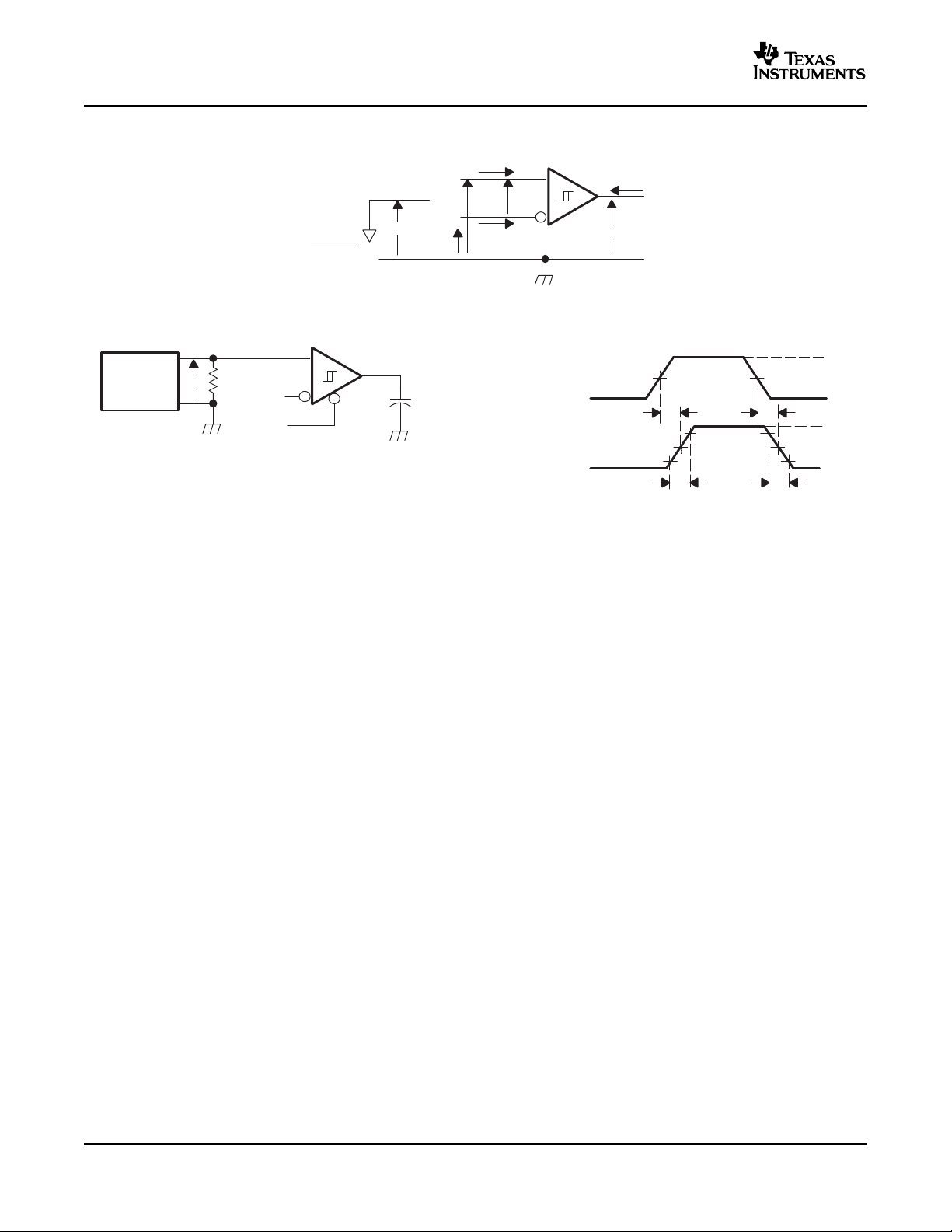
Figure 7. Receiver Voltage and Current Definitions
Figure 8. Receiver Switching Test Circuit and Voltage Waveforms
8
Submit Documentation Feedback

www.ti.com
50 Ω
Generator: PRR = 100 kHz,
50% Duty Cycle,
tr <6 ns, tf <6 ns, Zo = 50 Ω
V
O
RE
V
CC
0 V or 3 V
1.5 V 1.5 V
t
PZH(1)
t
PHZ
1.5 V
VOH –0.5 V
3 V
0 V
V
OH
≈ 0 V
V
O
CL = 15 pF ±20%
CL Includes Fixture and
Instrumentation Capacitance
V
I
DE
D
1 kΩ ± 1%
V
I
A
B
S1
D at 3 V
S1 to B
t
PZL(1)
t
PLZ
1.5 V
VOL +0.5 V
V
OL
V
O
D at 0 V
S1 to A
Input
Generator
R
3 V
A
B
V
CC
PARAMETER MEASUREMENT INFORMATION (continued)
SN65HVD05 , , SN65HVD06
SN75HVD05 , SN65HVD07
SN75HVD06 , SN75HVD07
SLLS533D – MAY 2002 – REVISED JULY 2006
Figure 9. Receiver Enable and Disable Time Test Circuit and Voltage Waveforms With Drivers Enabled
Submit Documentation Feedback
9

www.ti.com
1.5 V
t
PZH(2)
1.5 V
3 V
0 V
V
OH
GND
V
I
V
O
0 V or 1.5 V
1.5 V or 0 V
A at 1.5 V
B at 0 V
S1 to B
t
PZL(2)
1.5 V
V
OL
V
O
A at 0 V
B at 1.5 V
S1 to A
50 Ω
Generator: PRR = 100 kHz,
50% Duty Cycle,
tr <6 ns, tf <6 ns, Zo = 50 Ω
V
O
RE
CL = 15 pF ±20%
CL Includes Fixture and
Instrumentation Capacitance
V
I
DE
1 kΩ ± 1%
A
B
S1
Input
Generator
R
0 V
A
B
V
CC
V
CC
Pulse Generator,
15 µs Duration,
1% Duty Cycle
tr, tf ≤ 100 ns
100 Ω
± 1%
_
+
A
B
R
D
DE
RE
0 V or 3 V
NOTE: This test is conducted to test survivability only. Data stability at the R output is not specified.
3 V or 0 V
SN65HVD05 , , SN65HVD06
SN75HVD05 , SN65HVD07
SN75HVD06 , SN75HVD07
SLLS533D – MAY 2002 – REVISED JULY 2006
PARAMETER MEASUREMENT INFORMATION (continued)
10
Figure 10. Receiver Enable Time From Standby (Driver Disabled)
Figure 11. Test Circuit, Transient Over Voltage Test
Submit Documentation Feedback

www.ti.com
FUNCTION TABLES
DRIVER
INPUT ENABLE OUTPUTS
D DE A B
H H H L
L H L H
X L Z Z
Open H H L
X Open Z Z
SN65HVD05 , , SN65HVD06
SN75HVD05 , SN65HVD07
SN75HVD06 , SN75HVD07
SLLS533D – MAY 2002 – REVISED JULY 2006
RECEIVER
DIFFERENTIAL INPUTS ENABLE OUTPUT
VID= VA- V
VID≤ -0.2 V L L
-0.2 V < VID< -0.01 V L ?
-0.01 V ≤ V
Open Circuit L H
Short Circuit L H
(1) H = high level; L = low level; Z = high impedance; X = irrelevant;
? = indeterminate
B
ID
X H Z
X Open Z
(1)
RE R
L H
Submit Documentation Feedback
11

www.ti.com
9 V
1 kΩ
100 kΩ
Input
V
CC
D and RE Inputs
9 V
1 kΩ
100 kΩ
Input
V
CC
DE Input
16 V
16 V
100 kΩ
R3
R1
R2
Input
A Input
16 V
16 V
100 kΩ
R3
R1
R2
Input
B Input
16 V
16 V
V
CC
A and B Outputs
9 V
V
CC
R Output
5 Ω
Output
V
CC
SN65HVD05
SN65HVD06
SN65HVD07
R1/R2
9 kΩ
36 kΩ
36 kΩ
R3
45 kΩ
180 kΩ
180 kΩ
V
CC
Output
SN65HVD05 , , SN65HVD06
SN75HVD05 , SN65HVD07
SN75HVD06 , SN75HVD07
SLLS533D – MAY 2002 – REVISED JULY 2006
EQUIVALENT INPUT AND OUTPUT SCHEMATIC DIAGRAMS
12
Submit Documentation Feedback
www.ti.com
85
25
1 10 40
Maximum Recommended Still-Air
Operating Temperature - T
A
( °C
Signaling Rate - Mbps
)
High K Board
Low K Board
85
25
1 10
Maximum Recommended Still-Air
Operating Temperature - T
A
Signaling Rate - Mbps
( °C)
High K Board
Low K Board
30
40
50
60
70
80
90
100
110
120
0 5 10 15 20 25 30 35 40
I
CC
- RMS Supply Current - mA
TA = 25°C
RE at V
CC
DE at V
CC
R
L
= 54 Ω
CL = 50 pF
VCC = 5 V
Signaling Rate - Mbps
40
60
80
100
120
0 2.5 5 7.5 10
Signaling Rate - Mbps
I
CC
- RMS Supply Current - mA
TA = 25°C
RE at V
CC
DE at V
CC
R
L
= 54 Ω
CL = 50 pF
VCC = 5 V
SN65HVD05 , , SN65HVD06
SN75HVD05 , SN65HVD07
SN75HVD06 , SN75HVD07
SLLS533D – MAY 2002 – REVISED JULY 2006
TYPICAL CHARACTERISTICS
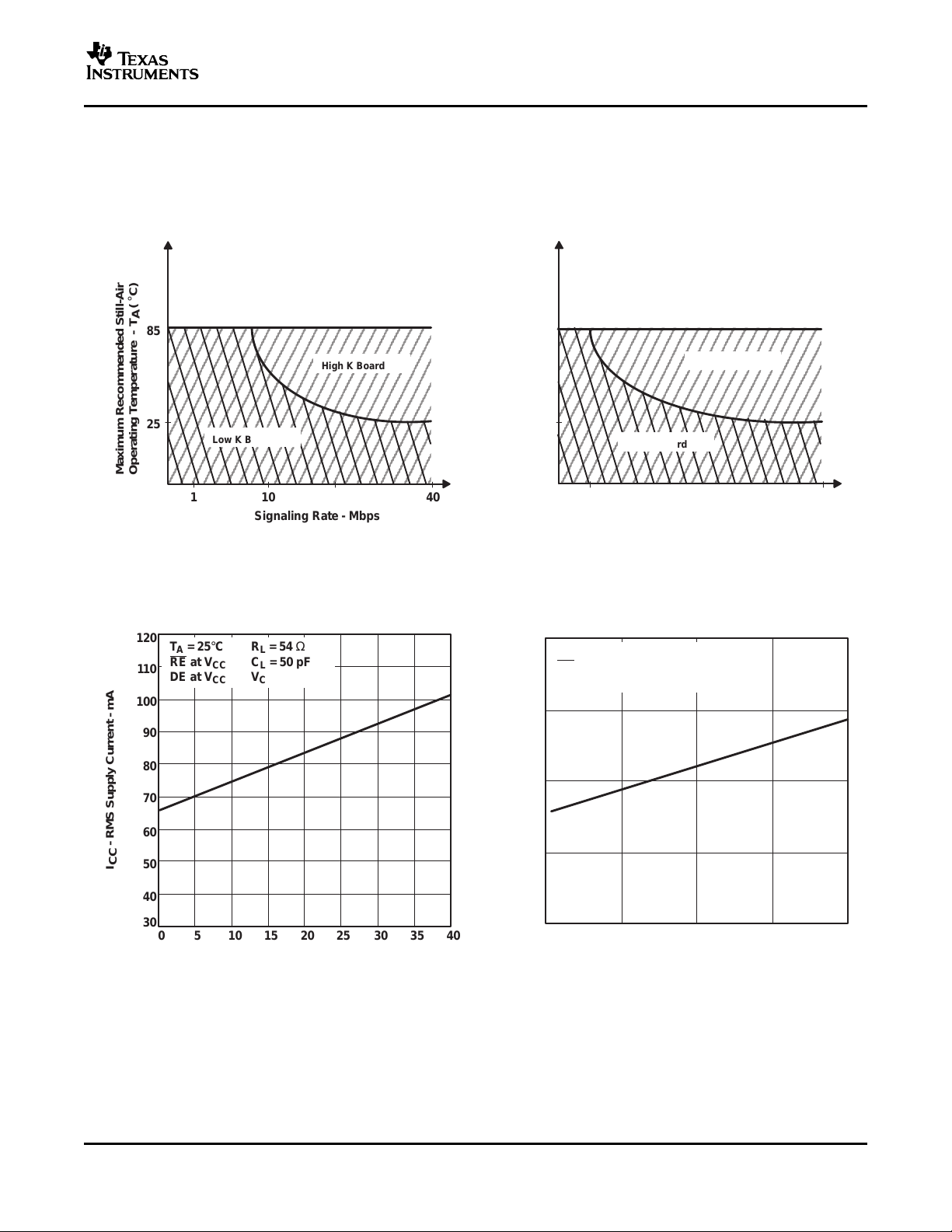
MAXIMUM RECOMMENDED STILL-AIR MAXIMUM RECOMMENDED STILL-AIR
HVD05 HVD06
OPERATING TEMPERATURE OPERATING TEMPERATURE
vs vs
SIGNALING RATE SIGNALING RATE
(D-PACKAGE) (D-PACKAGE)
Figure 12. Figure 13.
HVD05 HVD06
RMS SUPPLY CURRENT RMS SUPPLY CURRENT
vs vs
SIGNALILNG RATE SIGNALING RATE
Figure 14. Figure 15.
Submit Documentation Feedback
13

www.ti.com
40
50
60
70
80
90
100
110
100 400 700 1000
I
CC
- RMS Supply Current - mA
TA = 25°C
RE at V
CC
DE at V
CC
R
L
= 54 Ω
CL = 50 pF
VCC = 5 V
Signaling Rate - kbps
-7 -6 -5 -4 -3 -2 -1 0 1 2 3 4 5 6 7 8 9 1011 12
- Bus Input Current -I
I
Aµ
VI - Bus Input Voltage - V
TA = 25°C
DE at 0 V
VCC = 5 V
-200
-150
-100
-50
0
50
100
150
200
250
HVD05
HVD06
HVD07
-160
-140
-120
-100
-80
-60
-40
-20
0
0 0.5 1 1.5 2 4.52.5 3 3.5 4
- Driver High-Level Output Current - mA
I
OH
VO - High-Level Output Voltage - V
5
TA = 25°C
DE at V
CC
D at V
CC
VCC = 5 V
0 0.5 1 1.5 2 2.5 3 3.5 4 4.5 5
- Driver Low-Level Output Current - mA
I
OL
VO - Low-Level Output Voltage - V
0
20
40
60
80
100
120
140
160
TA = 25°C
DE at V
CC
D at 0 V
VCC = 5 V
SN65HVD05 , , SN65HVD06
SN75HVD05 , SN65HVD07
SN75HVD06 , SN75HVD07
SLLS533D – MAY 2002 – REVISED JULY 2006
TYPICAL CHARACTERISTICS (continued)
RMS SUPPLY CURRENT BUS INPUT CURRENT
DRIVER HIGH-LEVEL OUTPUT CURRENT DRIVER LOW-LEVEL OUTPUT CURRENT
HIGH-LEVEL OUTPUT VOLTAGE LOW-LEVEL OUTPUT VOLTAGE
HVD07
vs vs
SIGNALING RATE BUS INPUT VOLTAGE
Figure 16. Figure 17.
vs vs
14
Figure 18. Figure 19.
Submit Documentation Feedback

www.ti.com
0 0.6 1.2 1.8 2.4 3 3.6 4.2 4.8 5.4
0
10
20
30
40
50
60
70
I
O
- Driver Output Current - mA
VCC - Supply Voltage - V
TA = 25°C
DE at V
CC
D at V
CC
RL = 54 Ω
2
2.2
2.4
2.6
2.8
3
3.2
3.4
3.6
3.8
4
-40 -15
10 35 60 85
V
OD
- Differential Output Voltage - V
TA - Free-Air Temperature - °C
DE at V
CC
D at V
CC
V
CC
= 5 V
RL = 54 Ω
0
0.5
1
1.5
2
2.5
3
3.5
4
4.5
5
0 20 40 60 80 100 120
- Differential Output Voltage - VV
O
IOD - Differential Output Current - mA
60 Ω Load
Line
30 Ω Load
Line
TA = 25°C
DE at V
CC
D at V
CC
V
CC
= 5 V
0
100
400
500
600
-7 -2 3 8 13
HVD06
EnableTime − ns
V −
(TEST)
Common-ModeVoltage − V
200
300
HVD07
HVD5
TYPICAL CHARACTERISTICS (continued)
SN65HVD05 , , SN65HVD06
SN75HVD05 , SN65HVD07
SN75HVD06 , SN75HVD07
SLLS533D – MAY 2002 – REVISED JULY 2006
DIFFERENTIAL OUTPUT VOLTAGE DRIVER OUTPUT CURRENT
vs vs
FREE-AIR TEMPERATURE SUPPLY VOLTAGE
Figure 20. Figure 21.
DIFFERENTIAL OUTPUT VOLTAGE ENABLE TIME
vs vs
DIFFERENTIAL OUTPUT CURRENT COMMON-MODE VOLTAGE (SEE Figure 24 )
Figure 22. Figure 23.
Submit Documentation Feedback
15

www.ti.com
60 W
1%±
50 W
375 W 1%±
-7V<V <12V
(TEST)
V
OD
V (low)
OD
t (diff)
pZL
t (diff)
pZH
V
0or3V
375 W 1%±
50%
0V
1.5V
D
Z
DE
Y
-1.5V
V (high)
OD
Input
Generator
SN65HVD05 , , SN65HVD06
SN75HVD05 , SN65HVD07
SN75HVD06 , SN75HVD07
SLLS533D – MAY 2002 – REVISED JULY 2006
TYPICAL CHARACTERISTICS (continued)
The time t
Figure 24. Driver Enable Time From DE to V
(x) is the measure from DE to V
pZL
OD
(x). V
OD
is valid when it is greater than 1.5 V.
OD
16
Submit Documentation Feedback

www.ti.com
APPLICATION INFORMATION
R
T
R
T
Device
HVD05
HVD06
HVD07
Number of Devices on Bus
64
256
256
NOTE: The line should be terminated at both ends with its characteristic impedance (RT = ZO).
Stub lengths off the main line should be kept as short as possible.
Figure 25. Typical Application Circuit
SN65HVD05 , , SN65HVD06
SN75HVD05 , SN65HVD07
SN75HVD06 , SN75HVD07
SLLS533D – MAY 2002 – REVISED JULY 2006
Submit Documentation Feedback
17

PACKAGE OPTION ADDENDUM
www.ti.com
PACKAGING INFORMATION
Orderable Device Status
SN65HVD05D ACTIVE SOIC D 8 75 Green (RoHS &
SN65HVD05DG4 ACTIVE SOIC D 8 75 Green (RoHS &
SN65HVD05DR ACTIVE SOIC D 8 2500 Green (RoHS &
SN65HVD05DRG4 ACTIVE SOIC D 8 2500 Green (RoHS &
SN65HVD05P ACTIVE PDIP P 8 50 Pb-Free
SN65HVD05PE4 ACTIVE PDIP P 8 50 Pb-Free
SN65HVD06D ACTIVE SOIC D 8 75 Green (RoHS &
SN65HVD06DG4 ACTIVE SOIC D 8 75 Green (RoHS &
SN65HVD06DR ACTIVE SOIC D 8 2500 Green (RoHS &
SN65HVD06DRG4 ACTIVE SOIC D 8 2500 Green (RoHS &
SN65HVD06P ACTIVE PDIP P 8 50 Pb-Free
SN65HVD06PE4 ACTIVE PDIP P 8 50 Pb-Free
SN65HVD07D ACTIVE SOIC D 8 75 Green (RoHS &
SN65HVD07DG4 ACTIVE SOIC D 8 75 Green (RoHS &
SN65HVD07DR ACTIVE SOIC D 8 2500 Green (RoHS &
SN65HVD07DRG4 ACTIVE SOIC D 8 2500 Green (RoHS &
SN65HVD07P ACTIVE PDIP P 8 50 Pb-Free
SN65HVD07PE4 ACTIVE PDIP P 8 50 Pb-Free
SN75HVD05D ACTIVE SOIC D 8 75 Green (RoHS &
SN75HVD05DG4 ACTIVE SOIC D 8 75 Green (RoHS &
SN75HVD05DR ACTIVE SOIC D 8 2500 Green (RoHS &
SN75HVD05DRG4 ACTIVE SOIC D 8 2500 Green (RoHS &
SN75HVD05P ACTIVE PDIP P 8 50 Pb-Free
SN75HVD05PE4 ACTIVE PDIP P 8 50 Pb-Free
SN75HVD06D ACTIVE SOIC D 8 75 Green (RoHS &
(1)
Package
Type
Package
Drawing
Pins Package
Qty
Eco Plan
no Sb/Br)
no Sb/Br)
no Sb/Br)
no Sb/Br)
no Sb/Br)
no Sb/Br)
no Sb/Br)
no Sb/Br)
no Sb/Br)
no Sb/Br)
no Sb/Br)
no Sb/Br)
no Sb/Br)
no Sb/Br)
no Sb/Br)
no Sb/Br)
no Sb/Br)
(RoHS)
(RoHS)
(RoHS)
(RoHS)
(RoHS)
(RoHS)
(RoHS)
(RoHS)
(2)
Lead/Ball Finish MSL Peak Temp
CU NIPDAU Level-1-260C-UNLIM
CU NIPDAU Level-1-260C-UNLIM
CU NIPDAU Level-1-260C-UNLIM
CU NIPDAU Level-1-260C-UNLIM
CU NIPDAU N / A for Pkg Type
CU NIPDAU N / A for Pkg Type
CU NIPDAU Level-1-260C-UNLIM
CU NIPDAU Level-1-260C-UNLIM
CU NIPDAU Level-1-260C-UNLIM
CU NIPDAU Level-1-260C-UNLIM
CU NIPDAU N / A for Pkg Type
CU NIPDAU N / A for Pkg Type
CU NIPDAU Level-1-260C-UNLIM
CU NIPDAU Level-1-260C-UNLIM
CU NIPDAU Level-1-260C-UNLIM
CU NIPDAU Level-1-260C-UNLIM
CU NIPDAU N / A for Pkg Type
CU NIPDAU N / A for Pkg Type
CU NIPDAU Level-1-260C-UNLIM
CU NIPDAU Level-1-260C-UNLIM
CU NIPDAU Level-1-260C-UNLIM
CU NIPDAU Level-1-260C-UNLIM
CU NIPDAU N / A for Pkg Type
CU NIPDAU N / A for Pkg Type
CU NIPDAU Level-1-260C-UNLIM
16-Mar-2007
(3)
Addendum-Page 1

PACKAGE OPTION ADDENDUM
www.ti.com
Orderable Device Status
(1)
Package
Type
Package
Drawing
Pins Package
Qty
Eco Plan
(2)
SN75HVD06DG4 ACTIVE SOIC D 8 75 Green (RoHS &
Lead/Ball Finish MSL Peak Temp
CU NIPDAU Level-1-260C-UNLIM
16-Mar-2007
(3)
no Sb/Br)
SN75HVD06DR ACTIVE SOIC D 8 2500 Green (RoHS &
CU NIPDAU Level-1-260C-UNLIM
no Sb/Br)
SN75HVD06DRG4 ACTIVE SOIC D 8 2500 Green (RoHS &
CU NIPDAU Level-1-260C-UNLIM
no Sb/Br)
SN75HVD06P ACTIVE PDIP P 8 50 Pb-Free
CU NIPDAU N / A for Pkg Type
(RoHS)
SN75HVD06PE4 ACTIVE PDIP P 8 50 Pb-Free
CU NIPDAU N / A for Pkg Type
(RoHS)
SN75HVD07D ACTIVE SOIC D 8 75 Green (RoHS &
CU NIPDAU Level-1-260C-UNLIM
no Sb/Br)
SN75HVD07DG4 ACTIVE SOIC D 8 75 Green (RoHS &
CU NIPDAU Level-1-260C-UNLIM
no Sb/Br)
SN75HVD07DR ACTIVE SOIC D 8 2500 Green (RoHS &
CU NIPDAU Level-1-260C-UNLIM
no Sb/Br)
SN75HVD07DRG4 ACTIVE SOIC D 8 2500 Green (RoHS &
CU NIPDAU Level-1-260C-UNLIM
no Sb/Br)
SN75HVD07P ACTIVE PDIP P 8 50 Pb-Free
CU NIPDAU N / A for Pkg Type
(RoHS)
SN75HVD07PE4 ACTIVE PDIP P 8 50 Pb-Free
CU NIPDAU N / A for Pkg Type
(RoHS)
(1)
The marketing status values are defined as follows:
ACTIVE: Product device recommended for new designs.
LIFEBUY: TI has announced that the device will be discontinued, and a lifetime-buy period is in effect.
NRND: Not recommended for new designs. Device is in production to support existing customers, but TI does not recommend using this part in
a new design.
PREVIEW: Device has been announced but is not in production. Samples may or may not be available.
OBSOLETE: TI has discontinued the production of the device.
(2)
Eco Plan - The planned eco-friendly classification: Pb-Free (RoHS), Pb-Free (RoHS Exempt), or Green (RoHS & no Sb/Br) - please check
http://www.ti.com/productcontent for the latest availability information and additional product content details.
TBD: The Pb-Free/Green conversion plan has not been defined.
Pb-Free (RoHS): TI's terms "Lead-Free" or "Pb-Free" mean semiconductor products that are compatible with the current RoHS requirements
for all 6 substances, including the requirement that lead not exceed 0.1% by weight in homogeneous materials. Where designed to be soldered
at high temperatures, TI Pb-Free products are suitable for use in specified lead-free processes.
Pb-Free (RoHS Exempt): This component has a RoHS exemption for either 1) lead-based flip-chip solder bumps used between the die and
package, or 2) lead-based die adhesive used between the die and leadframe. The component is otherwise considered Pb-Free (RoHS
compatible) as defined above.
Green (RoHS & no Sb/Br): TI defines "Green" to mean Pb-Free (RoHS compatible), and free of Bromine (Br) and Antimony (Sb) based flame
retardants (Br or Sb do not exceed 0.1% by weight in homogeneous material)
(3)
MSL, Peak Temp. -- The Moisture Sensitivity Level rating according to the JEDEC industry standard classifications, and peak solder
temperature.
Important Information and Disclaimer:The information provided on this page represents TI's knowledge and belief as of the date that it is
provided. TI bases its knowledge and belief on information provided by third parties, and makes no representation or warranty as to the
accuracy of such information. Efforts are underway to better integrate information from third parties. TI has taken and continues to take
reasonable steps to provide representative and accurate information but may not have conducted destructive testing or chemical analysis on
incoming materials and chemicals. TI and TI suppliers consider certain information to be proprietary, and thus CAS numbers and other limited
information may not be available for release.
In no event shall TI's liability arising out of such information exceed the total purchase price of the TI part(s) at issue in this document sold by TI
to Customer on an annual basis.
Addendum-Page 2

PACKAGE MATERIALS INFORMATION
www.ti.com
TAPE AND REEL BOX INFORMATION
22-Sep-2007
Device Package Pins Site Reel
Diameter
(mm)
SN65HVD05DR D 8 SITE 27 330 0 6.4 5.2 2.1 8 12 Q1
SN65HVD06DR D 8 SITE 27 330 0 6.4 5.2 2.1 8 12 Q1
SN65HVD07DR D 8 SITE 27 330 0 6.4 5.2 2.1 8 12 Q1
SN75HVD05DR D 8 SITE 27 330 0 6.4 5.2 2.1 8 12 Q1
SN75HVD06DR D 8 SITE 27 330 0 6.4 5.2 2.1 8 12 Q1
SN75HVD07DR D 8 SITE 27 330 0 6.4 5.2 2.1 8 12 Q1
Reel
Width
(mm)
A0 (mm) B0 (mm) K0 (mm) P1
(mm)W(mm)
Pin1
Quadrant
Pack Materials-Page 1

PACKAGE MATERIALS INFORMATION
www.ti.com
22-Sep-2007
Device Package Pins Site Length (mm) Width (mm) Height (mm)
SN65HVD05DR D 8 SITE 27 342.9 336.6 0.0
SN65HVD06DR D 8 SITE 27 342.9 336.6 0.0
SN65HVD07DR D 8 SITE 27 342.9 336.6 0.0
SN75HVD05DR D 8 SITE 27 342.9 336.6 0.0
SN75HVD06DR D 8 SITE 27 342.9 336.6 0.0
SN75HVD07DR D 8 SITE 27 342.9 336.6 0.0
Pack Materials-Page 2

MECHANICAL DATA
MPDI001A – JANUARY 1995 – REVISED JUNE 1999
P (R-PDIP-T8) PLASTIC DUAL-IN-LINE
0.400 (10,60)
0.355 (9,02)
8
5
0.260 (6,60)
0.240 (6,10)
1
0.021 (0,53)
0.015 (0,38)
NOTES: A. All linear dimensions are in inches (millimeters).
B. This drawing is subject to change without notice.
C. Falls within JEDEC MS-001
4
0.070 (1,78) MAX
0.020 (0,51) MIN
0.200 (5,08) MAX
0.125 (3,18) MIN
0.100 (2,54)
0.010 (0,25)
Seating Plane
M
0.325 (8,26)
0.300 (7,62)
0.015 (0,38)
Gage Plane
0.010 (0,25) NOM
0.430 (10,92)
MAX
4040082/D 05/98
For the latest package information, go to http://www.ti.com/sc/docs/package/pkg_info.htm
POST OFFICE BOX 655303 • DALLAS, TEXAS 75265


IMPORTANT NOTICE
Texas Instruments Incorporated and its subsidiaries (TI) reserve the right to make corrections, modifications, enhancements,
improvements, and other changes to its products and services at any time and to discontinue any product or service without notice.
Customers should obtain the latest relevant information before placing orders and should verify that such information is current and
complete. All products are sold subject to TI’s terms and conditions of sale supplied at the time of order acknowledgment.
TI warrants performance of its hardware products to the specifications applicable at the time of sale in accordance with TI’s
standard warranty. Testing and other quality control techniques are used to the extent TI deems necessary to support this
warranty. Except where mandated by government requirements, testing of all parameters of each product is not necessarily
performed.
TI assumes no liability for applications assistance or customer product design. Customers are responsible for their products and
applications using TI components. To minimize the risks associated with customer products and applications, customers should
provide adequate design and operating safeguards.
TI does not warrant or represent that any license, either express or implied, is granted under any TI patent right, copyright, mask
work right, or other TI intellectual property right relating to any combination, machine, or process in which TI products or services
are used. Information published by TI regarding third-party products or services does not constitute a license from TI to use such
products or services or a warranty or endorsement thereof. Use of such information may require a license from a third party under
the patents or other intellectual property of the third party, or a license from TI under the patents or other intellectual property of TI.
Reproduction of TI information in TI data books or data sheets is permissible only if reproduction is without alteration and is
accompanied by all associated warranties, conditions, limitations, and notices. Reproduction of this information with alteration is an
unfair and deceptive business practice. TI is not responsible or liable for such altered documentation. Information of third parties
may be subject to additional restrictions.
Resale of TI products or services with statements different from or beyond the parameters stated by TI for that product or service
voids all express and any implied warranties for the associated TI product or service and is an unfair and deceptive business
practice. TI is not responsible or liable for any such statements.
TI products are not authorized for use in safety-critical applications (such as life support) where a failure of the TI product would
reasonably be expected to cause severe personal injury or death, unless officers of the parties have executed an agreement
specifically governing such use. Buyers represent that they have all necessary expertise in the safety and regulatory ramifications
of their applications, and acknowledge and agree that they are solely responsible for all legal, regulatory and safety-related
requirements concerning their products and any use of TI products in such safety-critical applications, notwithstanding any
applications-related information or support that may be provided by TI. Further, Buyers must fully indemnify TI and its
representatives against any damages arising out of the use of TI products in such safety-critical applications.
TI products are neither designed nor intended for use in military/aerospace applications or environments unless the TI products are
specifically designated by TI as military-grade or "enhanced plastic." Only products designated by TI as military-grade meet military
specifications. Buyers acknowledge and agree that any such use of TI products which TI has not designated as military-grade is
solely at the Buyer's risk, and that they are solely responsible for compliance with all legal and regulatory requirements in
connection with such use.
TI products are neither designed nor intended for use in automotive applications or environments unless the specific TI products
are designated by TI as compliant with ISO/TS 16949 requirements. Buyers acknowledge and agree that, if they use any
non-designated products in automotive applications, TI will not be responsible for any failure to meet such requirements.
Following are URLs where you can obtain information on other Texas Instruments products and application solutions:
Products Applications
Amplifiers amplifier.ti.com Audio www.ti.com/audio
Data Converters dataconverter.ti.com Automotive www.ti.com/automotive
DSP dsp.ti.com Broadband www.ti.com/broadband
Interface interface.ti.com Digital Control www.ti.com/digitalcontrol
Logic logic.ti.com Military www.ti.com/military
Power Mgmt power.ti.com Optical Networking www.ti.com/opticalnetwork
Microcontrollers microcontroller.ti.com Security www.ti.com/security
RFID www.ti-rfid.com Telephony www.ti.com/telephony
Low Power www.ti.com/lpw Video & Imaging www.ti.com/video
Wireless
Wireless www.ti.com/wireless
Mailing Address: Texas Instruments, Post Office Box 655303, Dallas, Texas 75265
Copyright © 2007, Texas Instruments Incorporated
 Loading...