


SN75FC1000B
1-GIGABIT FIBRE CHANNEL TRANSCEIVER
SLLS371 – FEBRUARY 2000
1
POST OFFICE BOX 655303 • DALLAS, TEXAS 75265
D
1.0625 Gigabits Per Second (Gbps) Fibre
Channel Transceiver Compatible With ANSI
X3T11 (FC-PH-0)
D
Designed to Support X3T11 10-Bit I/F
Specification
D
Transmits Serial Data up to 1.0625 Gbps
(100 Megabytes Per Second [MBps] of Data
Bandwidth)
D
Operates With 3.3-V Supply Voltage
D
Interfaces to Electrical Cables/Backplane or
with Optical Modules
D
PECL Voltage Differential Signaling Load,
1 V Typ with 50 Ω – 75 Ω
D
Receiver Differential Input Voltage
200 mV Minimum
D
64-Pin Quad Flat Pack With Thermally
Enhanced Package
D
5-V Tolerant I/O Terminals
description
The SN75FC1000B fibre channel transceiver provides for ultra high-speed bidirectional point-to-point data
transmission. This device supports the ANSI X3T11 Fibre Channel standard and the functional and timing
requirements of the proposed 10-bit interface specification generated by ANSI X3T11.
17 18 19
RC0
SYNC
GND_TTL
RD0
RD1
RD2
V
CC
_TTL
RD3
RD4
RD5
RD6
V
CC
_TTL
RD7
RD8
RD9
GND_TTL
48
47
46
45
44
43
42
41
40
39
38
37
36
35
34
33
20
1
2
3
4
5
6
7
8
9
10
11
12
13
14
15
16
GND_CMOS
TD0
TD1
TD2
V
CC
_CMOS
TD3
TD4
TD5
TD6
V
CC
_CMOS
TD7
TD8
TD9
GND_CMOS
GND_TX
TC1
21 22 23 24
DIN_RXP
63 62 61 60 5964 58
DOUT_TXP
DOUT_TXN
GND_CMOS
GND_A
RESERVED
LCKREFN
LOOPEN
GND_A
REFCLK
SYNCEN
GND_CMOS
56 55 5457
25 26 27 28 29
53 52
TC0
DIN_RXN
51 50 49
30 31 32
RBC1
RBC0
GND_A
GND_RX
RC1
GND_A
V
CC
_TX
V
CC
_A
V
CC
_CMOS
V
CC
_A
V
CC
_A
V
CC
_RX
V
CC
_A
V
CC
_A
V
CC
_A
V
CC
_A
V
CC
_A
V
CC
_A
PHD OR PJD PACKAGE
(TOP VIEW)
Please be aware that an important notice concerning availability, standard warranty, and use in critical applications of
Texas Instruments semiconductor products and disclaimers thereto appears at the end of this data sheet.
PRODUCTION DATA information is current as of publication date.
Products conform to specifications per the terms of Texas Instruments
standard warranty. Production processing does not necessarily include
testing of all parameters.
Copyright 2000, Texas Instruments Incorporated

SN75FC1000B
1-GIGABIT FIBRE CHANNEL TRANSCEIVER
SLLS371 – FEBRUARY 2000
2
POST OFFICE BOX 655303 • DALLAS, TEXAS 75265
description (continued)
The intended application of this device is to provide building blocks for developing point-to-point baseband data
transmission over controlled-impedance media of approximately 50 Ω to 75 Ω. The transmission media can be
printed-circuit board traces, back planes, cables, or fiber optical media. The ultimate rate and distance of data
transfer is dependent upon the attenuation characteristics of the media and the noise coupling to the
environment.
The SN75FC1000B performs the data serialization and deserialization (SERDES) functions for the fibre
channel physical layer interface. The transceiver operates at 1.0625 Gbps (typical), providing up to 100 MBps
of bandwidth over a copper or optical media interface. The serializer/transmitter accepts 8b/10b parallel
encoded data bytes. The parallel data bytes are serialized and transmitted differentially nonreturn-to-zero
(NRZ) at pseudo-ECL (PECL) voltage levels. The deserializer/receiver extracts clock information from the input
serial stream and deserializes the data, outputting a parallel 10-bit data byte. The 10-bit data bytes are output
with respect to two receive byte clocks (RBC0, RBC1) allowing a protocol device to clock the parallel bytes in
RBC clock rising edges.
The transceiver automatically locks onto incoming data without the need to prelock. However, the transceiver
can be commanded to lock to the externally supplied reference clock (REFCLK) as a reset function, if needed.
The SN75FC1000B provides an internal loopback capability for self-test purposes. Serial data from the
serializer is passed directly to the deserializer allowing the protocol device a functional self-check of the physical
interface.
The SN75FC1000B is characterized for operation from 0°C to 70°C.
SN75FC1000B
1-GIGABIT FIBRE CHANNEL TRANSCEIVER
SLLS371 – FEBRUARY 2000
3
POST OFFICE BOX 655303 • DALLAS, TEXAS 75265
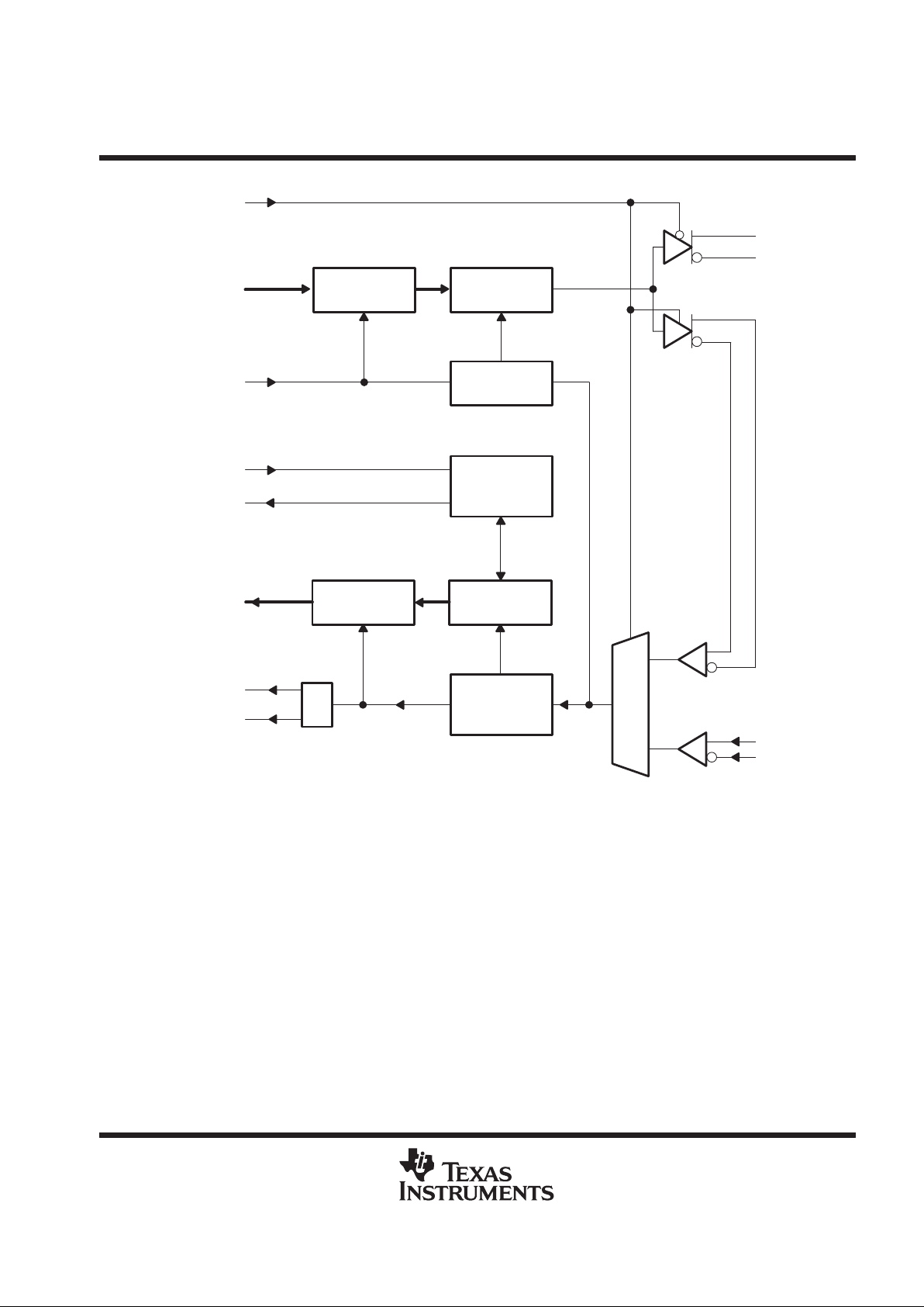
functional block diagram
LOOPEN
TD0 – TD9
10-Bit
Register
10
/
10
/
Shift
Register
REFCLK
Clock
Multiplier
2:1
MUX
Synchronous
Detect
SYNCEN
SYNC
RD0 – RD9
10-Bit
Register
10
/
10
/
Shift
Register
PLL Clock
Recovery and
Data Retiming
÷ 2
106.25 MHz
106.25 MHz
53 MHz
53 MHz
RBC0
RBC1
RX+
RX–
TX+
TX–
SN75FC1000B
1-GIGABIT FIBRE CHANNEL TRANSCEIVER
SLLS371 – FEBRUARY 2000
4
POST OFFICE BOX 655303 • DALLAS, TEXAS 75265
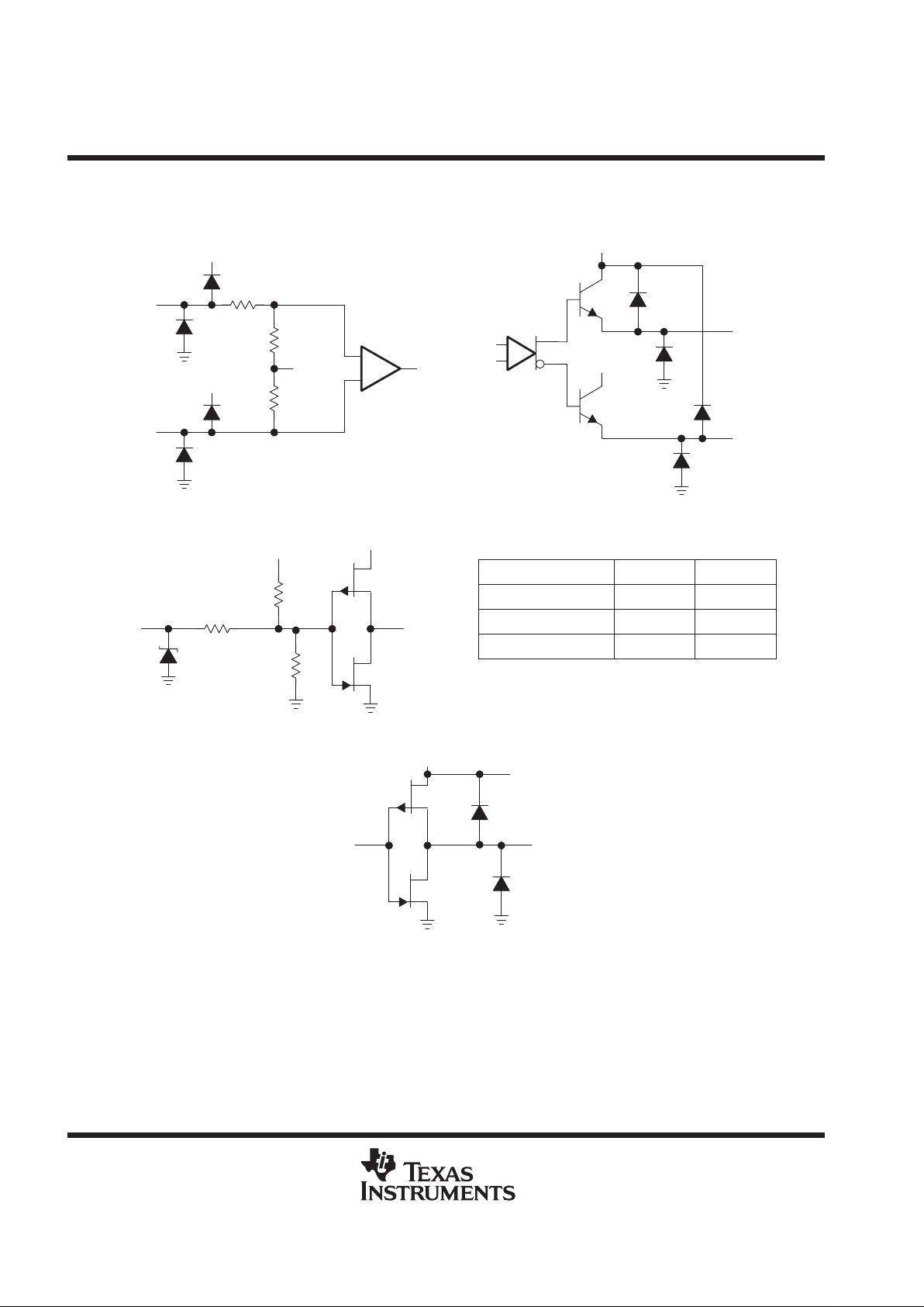
I/O structures
_
+
V
CM
V
DD
V
DD
100 Ω
4 kΩ
4 kΩ
DIN_RXP
DIN_RXN
V
DD
V
DD
DOUT_TXP
DOUT_TXN
PECL inputs (DIN_RXP, DIN_RXN) PECL outputs (DIN_TXP, DIN_TXN)
CMOS inputs (TD0 – TD9, LOOPEN, REFCLK, SYNCEN, LCKREFN)
V
DD
R2
R1
V
DD
120 Ω
Input
REFCLK, TD0 – TD9
LOOPEN
SYNCEN, LCKREFN
R1 R2
Open Circuit
Open Circuit
Open Circuit
Open Circuit
400 kΩ
400 kΩ
TERMINALS
P
N
CMOS outputs (RD0 – RD9, RBC0, RBC1, SYNC)
V
DD
Output
P
N

SN75FC1000B
1-GIGABIT FIBRE CHANNEL TRANSCEIVER
SLLS371 – FEBRUARY 2000
5
POST OFFICE BOX 655303 • DALLAS, TEXAS 75265
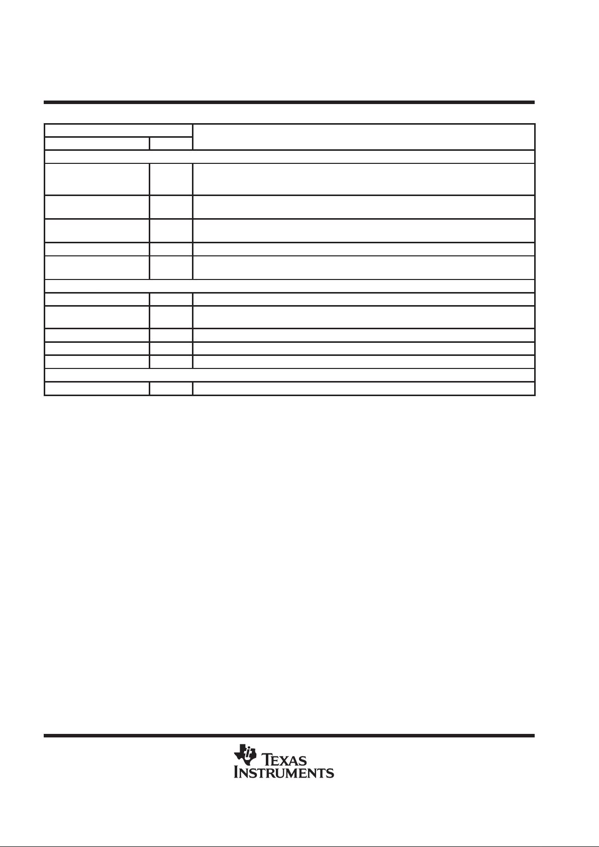
Terminal Functions
TERMINAL
NAME NO. TYPE
DESCRIPTION
I/O and DATA
DOUT_TXP
DOUT_TXN
62
61
Output Differential output transmit. DOUT_TXP and DOUT_TXN are differential serial outputs that interface
to a copper or an optical I/F module. These terminals transmit NRZ data at a rate of 1.0625 Gbps.
DOUT_TXP and DOUT_TXN are held static when LOOPEN is high and are active when LOOPEN is
low .
DIN_RXP
DIN_RXN
54
52
Input Differential input receive. DIN_RXP and DIN_RXN together are the differential serial input interface
from a copper or an optical I/F module. These terminals receive NRZ data at a rate of 1.0625 Gbps
and are active when LOOPEN is held low.
LCKREFN 27 Input Lock to reference. When LCKREFN is asserted low, the receive PLL phase locks to the supplied
REFCLK signal. LCKREFN prelocks or resets the receive PLL.
LOOPEN 19 Input Loop enable. When LOOPEN is high (active), the internal loop-back path is activated. The
transmitted serial data is directly routed to the inputs of the receiver. This provides a self-test
capability in conjunction with the protocol device. The DOUT_TXP and DOUT_TXN outputs are held
static during the loop-back test. LOOPEN is held low during standard operational state with external
serial outputs and inputs active.
RBC0
RBC1
31
30
Output Receive byte clock. RBC0 and RBC1 are 53.125-MHz recovered clocks used for synchronizing the
10-bit output data on RD0 – RD9. The 10-bit output data words are valid on the rising edges of RBC0
and RBC1. These clocks are adjusted to half-word boundaries in conjunction with synchronous
detect. The clocks are always expanded during data realignment and never slivered or truncated.
RBC0 registers bytes 1 and 3 of received data. RBC1 registers bytes 0 and 2 of received data.
RC1,
RC0
49
48
Analog Receive capacitor. RC0 and RC1 are external capacitor connections used for the receiver internal
PLL filter. The recommend value for this external capacitor is 2 nF.
RD0 – RD9 45,44,43,41,
40,39,38,36,
35,34
Output Receive data. These outputs carry 10-bit parallel data output from the transceiver to the protocol
layer. The data is referenced to terminals RBC0 and RBC1. Received data byte 0, which contains the
K28.5 character, is byte aligned to the rising edge of RBC1. RD0 is the first bit received.
REFCLK 22 Input Reference clock. REFCLK is an external 106.25 MHz input clock that synchronizes the receiver and
transmitter interfaces. The transmitter uses this clock to register the 10-bit input data (TD0..TD9) for
serialization. REFCLK is also used as a RX PLL preset or reference when LCKREFN is enabled.
SYNC 47 Output Synchronous detect. SYNC is asserted high upon detection of the K28.5 character in the serial data
path. SYNC is a high level for 1/2 REFCLK period. SYNC pulses are output only when SYNCEN is
activated (asserted high).
SYNCEN 24 Input Synchronous function enable. When SYNCEN is asserted high, the internal synchronization
function is activated. When this function is enabled, the transceiver detects the K28.5 character
(0011111010 negative beginning disparity) in the serial data stream and realigns data on byte
boundaries if required. When SYNCEN is low, serial input data is unframed in RD0 – RD9.
TC1
TC0
16
17
Analog T ransmit capacitor. TC0 and TC1 are external capacitor connections used for the transmitter internal
PLL filter. The recommended value of this external capacitor is 2 nF.
TD0 – TD9 2,3,4,6
7,8,9,1 1
12,13
Input Transmit data. These inputs carry 10-bit parallel data output from a protocol device to the transceiver
for serialization and transmission. This 10-bit parallel data is clocked into the transceiver on the rising
edge of REFCLK and transmitted as a serial stream with TD0 sent as the first bit.
SN75FC1000B
1-GIGABIT FIBRE CHANNEL TRANSCEIVER
SLLS371 – FEBRUARY 2000
6
POST OFFICE BOX 655303 • DALLAS, TEXAS 75265
Terminal Functions (Continued)
TERMINAL
NAME NO. TYPE
DESCRIPTION
POWER
VCC_A 20,28,29,53
55,57,59,60
63
Supply Analog power. VCC_A provides a supply reference voltage for the high-speed analog circuits.
VCC_CMOS 5,10,23, Supply Digital PECL logic power. VCC_CMOS provides an isolated low-noise power supply for the logic
circuits.
VCC_RX 50 Supply Receiver power. VCC_RX provides a low-noise supply reference voltage for the receiver high-speed
analog circuits.
VCC_TTL 42,37 Supply TTL power. VCC_TTL provides a supply reference voltage for the receiver TTL circuits.
VCC_TX 18 Supply Transmitter power. VCC_TX provides a low-noise supply reference voltage for the transmitter
high-speed analog circuits.
GROUND
GND_A 21,32,56,64 Ground Analog ground. GND_A provides a ground reference for the high-speed analog circuits.
GND_CMOS 1,14,
25,58
Ground Digital PECL logic ground. GND_CMOS provides an isolated low-noise ground for the logic circuits.
GND_RX 51 Ground Receiver ground. GND_RX provides a ground reference for the receiver circuits.
GND_TTL 33,46 Ground TTL circuit ground. GND_TTL provides a ground for TTL interface circuits.
GND_TX 15 Ground Transmitter ground. GND_TX provides a ground reference for the transmitter circuits.
MISCELLANEOUS
RESERVED 26 Reserved. Internally pulled to GND, leave open or assert low.
detailed description
data transmission
The transmitter registers incoming 10-bit-wide data words (8b/10b encoded data, TD0 – TD9) on the rising edge
of REFCLK (106.25 MHz). The reference clock is also used by the serializer, which multiplies the clock by a
factor of 10 providing a 1.0625 Gbaud signal that is fed to the shift register. The data is then transmitted
differentially at PECL voltage levels. The 8b/10b encoded data is transmitted sequentially bit 0 through 9.
transmission latency
The data transmission latency of the SN75FC1000B is defined as the delay from the initial 10-bit word load to
the serial transmission of bit 9. The typical transmission latency is 13 ns.
data reception
The receiver of the SN75FC1000B deserializes 1.0625 Gbps differential serial data. The 8b/10b data (or
equivalent) is retimed based on an extracted clock from the serial data. The serial data is then aligned to the
10-bit word boundaries and presented to the protocol controller along with two receive byte clocks (RBC0,
RBC1). RBC0 and RBC1 are 180 degrees out of phase and are generated by dividing down the recovered
1.0625 Gbps (531 MHz) clock by 10 providing for two 53-MHz signals. The receiver presents the protocol device
byte 0 of the received data valid on the rising edge of RBC1.
NOTE:
This allows the option of byte alignment without the use of the synchronous detection
(SYNC) function by the protocol device.
The receiver PLL can lock to the incoming 1.0625 GHz data without the need for a lock-to-reference preset. The
received serial data rate (RX+ and RX–) should be 1.0625 Gbps ±0.01% (100 ppm) for proper operation.
 Loading...