

SN75DP129
www.ti.com
SLAS583A – JANUARY 2008 – REVISED MARCH 2008
DisplayPort to TMDS Translator
1
FEATURES APPLICATIONS
• DisplayPort Physical Layer Input Port to TMDS
Physical Layer Output Port
• Integrated TMDS Level Translator With
Receiver Equalization
• Supports Data Rates up to 2.5 Gbps
• Integrated I2C Logic Block for DVI / HDMI
Connector Recognition
• Integrated Active I2C Buffer
• Enhanced ESD: 12 kV on all Pins
• Enhanced Commercial Temperature Range:
0 ° C to 85 ° C
• 36 Pin 6 × 6 QFN Package
DESCRIPTION
The SN75DP129 is a Dual-Mode DisplayPort input to Transition-Minimized Differential Signaling (TMDS) output.
The TMDS output has a built-in level translator, compliant with Digital Visual Interface 1.0 (DVI) and High
Definition Multimedia Interface 1.3 (HDMI) standards. The SN75DP129 is specified up to a maximum data rate of
2.5 Gbps, supporting resolutions greater then 1920 x 1200 or HDTV 12-bit color depth at 1080p (progressive
scan).
An integrated Active I2C buffer isolates the capacitive loading of the source system from that of the sink and
interconnecting cable. This isolation improves overall signal integrity of the system and provides greater design
margin within the source system for DVI / HDMI compliance testing.
A logic block was designed into the SN75DP129 to assist with TMDS connector identification. Through the use of
the I2C_EN pin, this logic block can be enabled to indicate the translated port is an HDMI port; therefore legally
supporting HDMI content.
• Personal Computer Market
– DP/TMDS Hardware Key (Dongle)
– Desktop PC
– Notebook PC
– Docking Station
– Standalone Video Card
1
Please be aware that an important notice concerning availability, standard warranty, and use in critical applications of Texas Instruments semiconductor products and disclaimers thereto appears at the end of this data sheet.
PRODUCTION DATA information is current as of publication date.
Products conform to specifications per the terms of the Texas
Instruments standard warranty. Production processing does not
necessarily include testing of all parameters.
Copyright © 2008, Texas Instruments Incorporated
www.ti.com
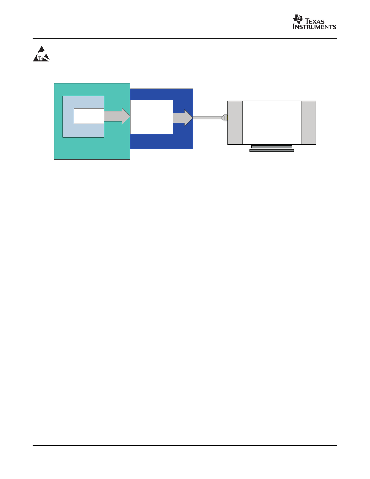
Dongle
Computer Notebook
DockingStation
GPU
SN75DP129
TMDSBuffer
DVIorHDMI
Compliant
MonitororHDTV
DP++
TMDS
SN75DP129
SLAS583A – JANUARY 2008 – REVISED MARCH 2008
These devices have limited built-in ESD protection. The leads should be shorted together or the device placed in conductive foam
during storage or handling to prevent electrostatic damage to the MOS gates.
TYPICAL APPLICATION
GPU — Graphics Processing Unit
DP++ — Dual-Mode DisplayPort
TMDS — Transition-Minimized Differential Signaling
DVI — Digital Visual Interface
HDMI — High Definition Multimedia Interface
2 Submit Documentation Feedback Copyright © 2008, Texas Instruments Incorporated
Product Folder Link(s): SN75DP129

www.ti.com
INTERNAL DATA CONNECTION DIAGRAM
GND
LP
TMDS_2(n)
VSadj
SDA
SCL
HPD_IN
VDD
HPD_OUT
GND
VCC
ML_IN0(p)
I2C_EN
VCC
I2C
Slave
TMDS_2(p)
ML_IN0(n)
ML_IN1(p)
ML_IN1(n)
VCC
ML_IN2(p)
ML_IN2(n)
GND
ML_IN3(p)
ML_IN3(n)
VCC
GND
TMDS_CLK(n)
TMDS_CLK(p)
VCC
TMDS_0(n)
TMDS_0(p)
GND
TMDS_1(n)
TMDS_1(p)
SN75DP129
AUX_I C(p)
2
1
AUX_I C(n)
2
1
SN75DP129
SLAS583A – JANUARY 2008 – REVISED MARCH 2008
(1) I2C bus data (n-SDA) and clock (p-SCL) lines.
Copyright © 2008, Texas Instruments Incorporated Submit Documentation Feedback 3
Product Folder Link(s): SN75DP129
www.ti.com
1
I2C_EN
VDD
ML_IN0(p)
HPD_OUT
SDA
VSadj
VCC
TMDS_2(n)
SCL
2 3 4 5 6 7 8
11
10
12
13
14
15
16
17
35
36
34
33
32
31
30
29
2627 24 23 22 21 2025
9
18
19
28
GND
VCC
LP
TMDS_2(p)
ML_IN0(n)
ML_IN1(p)
ML_IN1(n)
VCC
ML_IN2(p)
ML_IN2(n)
GND
ML_IN3(p)
ML_IN3(n)
VCC
GND
HPD_IN
GND
TMDS_CLK(n)
TMDS_CLK(p)
VCC
TMDS_0(n)
TMDS_0(p)
GND
TMDS_1(n)
TMDS_1(p)
SN75DP129
RHHPACKAGE
(TopView)
AUX_I2C(p)
1
AUX_I2C(n)
1
SN75DP129
SLAS583A – JANUARY 2008 – REVISED MARCH 2008
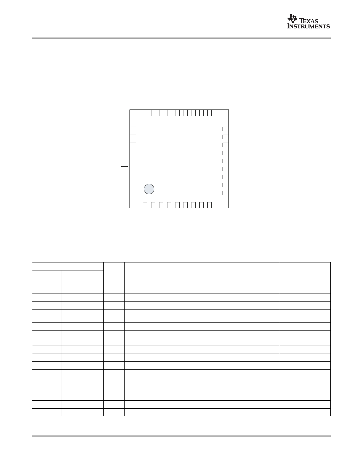
PIN CONFIGURATION
(1) I2C bus data (n-SDA) and clock (p-SCL) lines.
TERMINAL FUNCTIONS
TERMINAL
NAME NO.
2C(2)
AUX_I
GND 6, 10, 19, 25, 36 Ground Ground
HPD_IN 15 I Hot Plug Detect (HPD) Input Hot Plug Detect
HPD_OUT 13 O Hot Plug Detect (HPD) Output Hot Plug Detect
I2C_EN 32 I Control
LP 33 I Low Power Select Bar Control
ML_IN 0 34(p), 35(n) I DisplayPort Main Link Channel 0 Differential Input Main Link Input Pins
ML_IN 1 1(p), 2(n) I DisplayPort Main Link Channel 1 Differential Input Main Link Input Pins
ML_IN 2 4(p), 5(n) I DisplayPort Main Link Channel 2 Differential Input Main Link Input Pins
ML_IN 3 7(p), 8(n) I DisplayPort Main Link Channel 3 Differential Input Main Link Input Pins
TMDS_2 30(p), 29(n) O TMDS Data 2 Differential Output Main Link Output
TMDS_1 27(p), 26(n) O TMDS Data 1 Differential Output Main Link Output
TMDS_0 24(p), 23(n) O TMDS Data 0 Differential Output Main Link Output
TMDS_CLK 21(p), 20(n) O TMDS Data Clock Differential Output Main Link Output
SCL 17 I/O TMDS Port Bidirectional I2C Clock Line DDC Link (Sink)
SDA 16 I/O TMDS Port Bidirectional I2C Data Line DDC Link (Sink)
VCC 3, 9, 18, 22, 28 3.3 V Supply Voltage Supply
(1) (p) Positive; (n) Negative
(2) I2C bus data (n-SDA) and clock (p-SCL) lines.
(1)
11(p), 12(n) I/O Source Side Bidirectional DisplayPort Auxiliary Data Line DDC LINK (Source)
I/O DESCRIPTION TYPE
Internal I2C register enable, used for HDMI / DVI connector
differentiation
4 Submit Documentation Feedback Copyright © 2008, Texas Instruments Incorporated
Product Folder Link(s): SN75DP129
www.ti.com
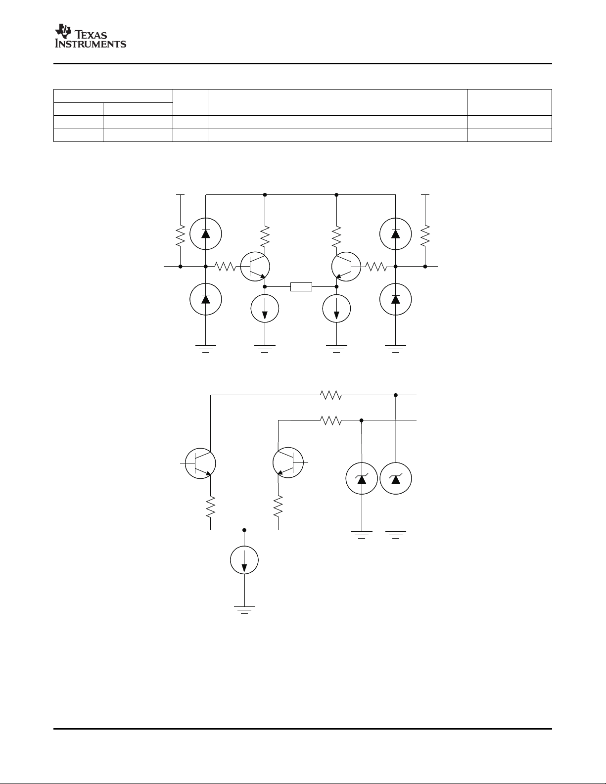
+
–
V
CC
50 W 50 W
V
TERM
V
TERM
Z
Y
10mA
SLAS583A – JANUARY 2008 – REVISED MARCH 2008
TERMINAL FUNCTIONS (continued)
TERMINAL
NAME NO.
VDD 14 HPD Supply Voltage Supply
VSadj 31 I TMDS-Compliant Voltage Swing Control Reference
(1)
I/O DESCRIPTION TYPE
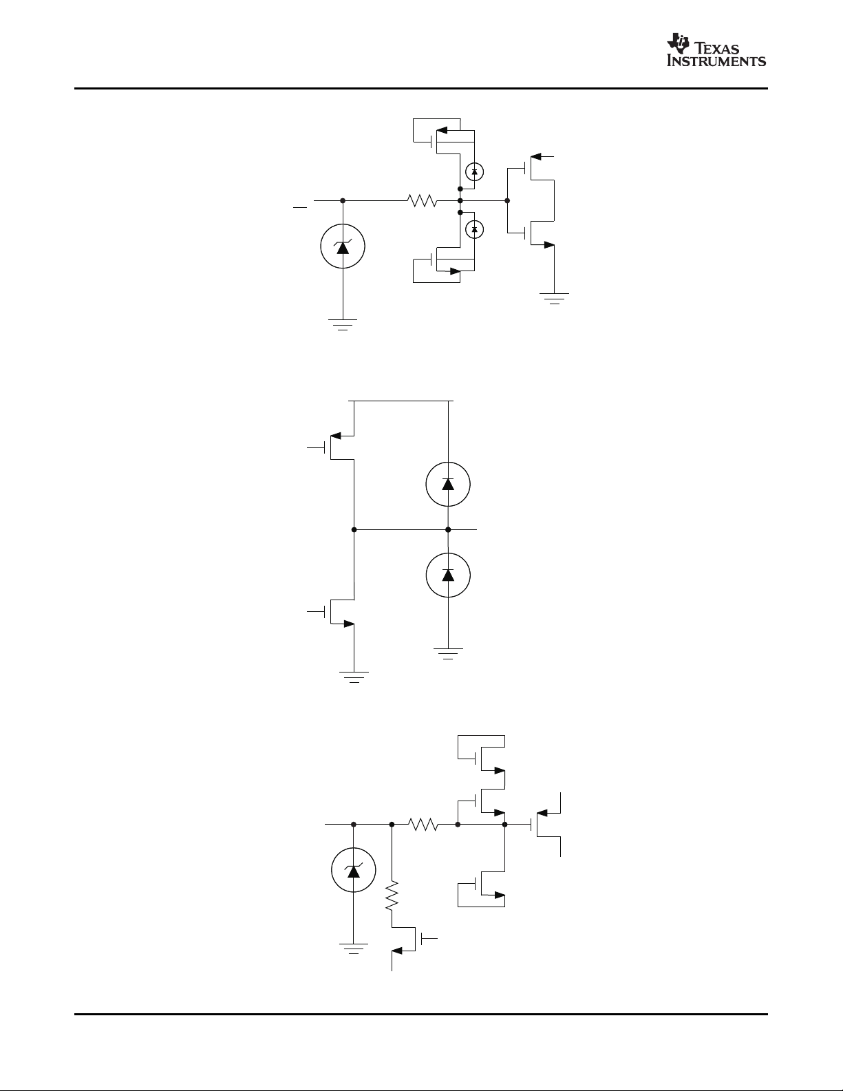
Input/Output Equivalent Circuits
SN75DP129
Figure 1. DisplayPort Input Stage
Figure 2. TMDS Output Stage
Copyright © 2008, Texas Instruments Incorporated Submit Documentation Feedback 5
Product Folder Link(s): SN75DP129
www.ti.com
I C_EN
2
LP
HPD_OUT
V
DD
SCL
SDA
AUX+/–
400 W
V
OL
SN75DP129
SLAS583A – JANUARY 2008 – REVISED MARCH 2008
Figure 3. HPD and Control Input Stage
Figure 4. HPD Output Stage
Figure 5. I2C Input and Output Stage
6 Submit Documentation Feedback Copyright © 2008, Texas Instruments Incorporated
Product Folder Link(s): SN75DP129
www.ti.com
Table 1. Control Pin Lookup Table
SIGNAL LEVEL STATE DESCRIPTION
H Normal Mode Normal operational mode for device
LP
L Low Power Mode
H HDMI
I2C_EN
L DVI
VS
adj
4.65 k Ω Driver output voltage swing precision control to aid with system compliance.
(1) (H) Logic High; (L) Logic Low
Compliant Voltage
Swing
Device is forced into a Low Power state causing the outputs to go to a high impedance
state. All other inputs are ignored.
Internal I2C register is active and readable, indicating the connector in use is
HDMI-compliant.
Internal I2C register is disabled and unreadable, indicating the connector in use is
DVI-compliant.
SN75DP129
SLAS583A – JANUARY 2008 – REVISED MARCH 2008
(1)
ORDERING INFORMATION
(1)
PART NUMBER PART MARKING PACKAGE
SN75DP129RHHR DP129 36-pin QFN Reel (large)
SN75DP129RHHT DP129 36-pin QFN Reel (small)
(1) For the most current package and ordering information, see the Package Option Addendum at the end of this document, or see the TI
web site at www.ti.com .
ABSOLUTE MAXIMUM RATINGS
over operating free-air temperature range (unless otherwise noted)
Supply voltage range
Supply voltage range VDD – 0.3 to 3.6 V
Voltage range HPD I/O – 0.3 to 5.5 V
Electrostatic discharge Charged-device model
Continuous power dissipation See Dissipation Ratings Table
(1) Stresses beyond those listed under absolute maximum ratings may cause permanent damage to the device. These are stress ratings
only and functional operation of the device at these or any conditions beyond those indicated under recommended operating conditions
is not implied. Exposure to absolute-maximum-rated conditions for extended periods may affect device reliability.
(2) All voltage values, except differential voltages, are with respect to network ground terminal.
(3) Tested in accordance with JEDEC Standard 22, Test Method A114-B
(4) Tested in accordance with JEDEC Standard 22, Test Method C101-A
(5) Tested in accordance with JEDEC Standard 22, Test Method A115-A
(2)
VCC – 0.3 to 3.6 V
Main link I/O (ML_IN x, DP_SINK x) differential voltage 1.5 V
TMDS I/O – 0.3 to 4 V
Auxiliary I/O – 0.3 to 5.5 V
Control I/O – 0.3 to 5.5 V
Human body model
Machine model
(3)
(4)
(5)
(1)
VALUE UNIT
± 12000 V
± 1000 V
± 200 V
DISSIPATION RATINGS
PACKAGE TA≤ 25 ° C
36-pin QFN (RHH)
PCB JEDEC
STANDARD
Low-K 1398 mW 13.98 mW/ ° C 559 mW
High-K 2941 mW 29.41 mW/ ° C 1176 mW
DERATING FACTOR
ABOVE TA= 25 ° C POWER RATING
(1) This is the inverse of the junction-to-ambient thermal resistance when board-mounted and with no air flow.
Copyright © 2008, Texas Instruments Incorporated Submit Documentation Feedback 7
Product Folder Link(s): SN75DP129
(1)
TA= 85 ° C
www.ti.com
SN75DP129
SLAS583A – JANUARY 2008 – REVISED MARCH 2008
THERMAL CHARACTERISTICS
over operating free-air temperature range (unless otherwise noted)
PARAMETER TEST CONDITIONS MIN TYP MAX UNIT
R
Junction-to-board thermal resistance 9.44
θ JB
R
Junction-to-case thermal resistance 24.74 ° C/W
θ JC
P
Device power dissipation
D
P
Device power dissipation under low power LP = 0 V 5 20 µ W
SD
(2)
(1) The maximum rating is simulated under 3.6 V V
(2) Power disipation is the sum of the power consumption from the V
Termination Supply).
RECOMMENDED OPERATING CONDITIONS
V
CC
V
DD
T
A
MAIN LINK DIFFERENTIAL INPUT PINS
V
ID
d
R
TMDS DIFFERENTIAL OUTPUT PINS
AV
d
R
R
t
AUXILIARY AND I2C PINS
V
I
d
R(I2C)
HPD AND CONTROL PINS
V
IH
V
IL
Supply voltage 3 3.3 3.6 V
Supply voltage 1.65 3.6 V
Operating free-air temperature 0 85 ° C
Peak-to-peak input differential voltage 0.15 1.40 V
Data rate 2.5 Gbps
TMDS output termination voltage 3 3.3 3.6 V
CC
Data rate 2.5 Gbps
Termination resistance 45 50 55 Ω
Input voltage 0 5.5 V
I2C data rate 100 kHz
High-level input voltage 2 5.5 V
Low-level input voltage 0 0.8 V
LP = 3.3 V, ML: VID= 500 mV, 2.5 Gbps
PRBS; 380 490 mW
I2C: VID= 3.3 V, 100 Kbps PRBS; HPD = 5 V
and V
CC
unless otherwise noted.
DD
(1)
and V
CC
pins, plus the 132 mW of power from the AVCC (Receiver
DD
° C/W
MIN NOM MAX UNIT
Device Power
The SN75DP129 is designed to operate from one or two supply voltages, depending on the implementation of
the integrated Hot Plug Detect (HPD) level translator. The TMDS level translator is powered from a single 3.3-V
supply. The HPD translator is powered using the VDD pin and its voltage can range from 1.8 V to 3.3 V. This
voltage determines the HIGH-level output voltage of the HPD_OUT pin.
ELECTRICAL CHARACTERISTICS
over recommended operating conditions (unless otherwise noted)
PARAMETER TEST CONDITIONS MIN TYP MAX UNIT
I
I
ISD Shutdown current LP = 0 V 1 5 µ A
8 Submit Documentation Feedback Copyright © 2008, Texas Instruments Incorporated
Supply current LP = 3.6 V, V
CC
= VDD, 50 75 112 mA
CC
ML: VID= 500 mV, 2.7 Gbps PRBS
Supply current 1 2 mA
DD
AUX: VI= 3.3 V, 100 kHz PRBS
HPD: HPD_IN = 5 V
Product Folder Link(s): SN75DP129

www.ti.com
DP129
100kW
HPDInput
HPDOutput
100kW
t
PD(HPD)
50%
50%
5V
0V
V
DD
0V
HPD_IN
HPD_OUT
SN75DP129
SLAS583A – JANUARY 2008 – REVISED MARCH 2008
Hot Plug and Cable Adapter Detect
The SN75DP129 has a built-in level shifter for the HPD outputs. The output voltage level of the HPD pin is
defined by the voltage level of the VDD pin.
ELECTRICAL CHARACTERISTICS
over recommended operating conditions (unless otherwise noted)
PARAMETER TEST CONDITIONS MIN TYP MAX UNIT
V
OH3.3
V
OH2.5
V
OH1.8
V
OL
I
H
I
L
High-level output voltage IOH= – 100 A, V
Low-level output voltage IOH= 100 µ A 0 0.4 V
High-level input current VIH= 2.0 V, V
Low-level input current VIL= 0.8 V, V
SWITCHING CHARACTERISTICS
over recommended operating conditions (unless otherwise noted)
PARAMETER TEST CONDITIONS MIN TYP MAX UNIT
t
PD(HPD)
Propagation delay V
IOH= – 100 µ A, V
IOH= – 100 A, V
= 3.6 V 5 30 ns
DD
= 3.3 V 3 3.3 V
DD × 1
= 2.5 V 2.25 2.5 V
DD × 1
= 1.8 V 1.62 1.8 V
DD × 1
= 3.6 V – 10 10 µ A
DD
= 3.6 V – 10 10 µ A
DD
Figure 6. HPD Test Circuit
Figure 7. HPD Timing Diagram
AUX / I2C Pins
The SN75DP129 utilizes an active I2C repeater. The repeater isolates the parasitic effects of the system to aid
with system level compliance.
In addition to the I2C repeater, the SN75DP129 supports the connector detection I2C register. This register is
Product Folder Link(s): SN75DP129
enabled using the I2C_EN pin. When active, an internal memory register is readable using the AUX_I
This I2C register block functionality is described in the APPLICATION INFORMATION section.
Copyright © 2008, Texas Instruments Incorporated Submit Documentation Feedback 9
2
C pins.
 Loading...