

1
FEATURES
APPLICATIONS
DESCRIPTION
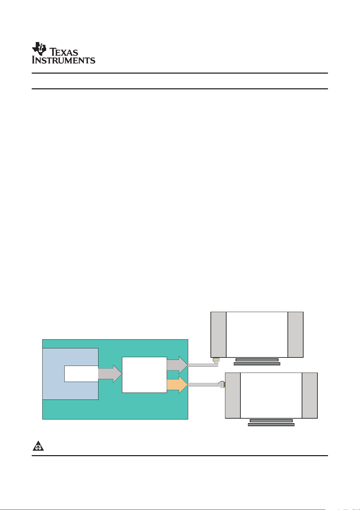
TYPICAL APPLICATION
Computer/Notebook/DockingStation
GPU
DP++
SN75DP122
DP++
TMDS
DisplayPort
Enabled
MonitororHDTV
HDMI / DVI
MonitororHDTV
SN75DP122
SLLS892 – FEBRUARY 2008
www.ti.com
DisplayPort 1:2 Switch With Integrated TMDS Translator
• One Input Port to One of Two Output Ports – 12 kV on all High Speed Pins
• Integrated TMDS Level Translator with – 8 kV on all Auxiliary and I2C Pins
Receiver Equalization
• Enhanced Commercial Temperature Range:
• DP Port Supports Data Rates up to 2.7 Gbps
0 ° C to 85 ° C
• DP Port Supports Dual-Mode DisplayPort
• 56 Pin 8 × 8 QFN Package
• DP Port Output Waveform Mimics Input
Waveform Characteristics
• Personal Computer Market
• TMDS Port Supports Data Rates up to 2.5
– Desktop PC
Gbps
– Notebook PC
• Integrated I2C Logic Block for DVI/HDMI
– Docking Station
Connector Recognition
– Standalone Video Card
• Enhanced ESD:
The SN75DP122 is a one Dual-Mode DisplayPort input to one Dual-Mode DisplayPort output or one TMDS
output. The TMDS output has a built in level translator compliant with Digital Video Interface (DVI) 1.0 and High
Definition Multimedia Interface (HDMI) 1.3b. The DisplayPort output follows the input signal in a manner that
provides the highest level of signal integrity while supporting the EMI benefits of spread spectrum clocking.
Through the SN75DP122 data rates of up to 2.7 Gbps through each link for a total throughput of up to 10.8 Gbps
can be realized.
In addition to the switching of the DisplayPort high speed signal lines, the SN75DP122 also supports the
switching of the bidirectional auxiliary (AUX), Hot Plug Detect (HPD), and Cable Adapter Detect (CAD) channels.
The Auxiliary differential pair supports Dual-Mode DisplayPort operation through the DisplayPort port. Through
the TMDS port the auxiliary port is configured as an I2C port with an integrated I2C repeater.
The SN75DP122 is characterized for operation over ambient air temperature of 0 ° C to 85 ° C.
1
Please be aware that an important notice concerning availability, standard warranty, and use in critical applications of
Texas Instruments semiconductor products and disclaimers thereto appears at the end of this data sheet.
PRODUCTION DATA information is current as of publication date.
Copyright © 2008, Texas Instruments Incorporated
Products conform to specifications per the terms of the Texas
Instruments standard warranty. Production processing does not
necessarily include testing of all parameters.
www.ti.com
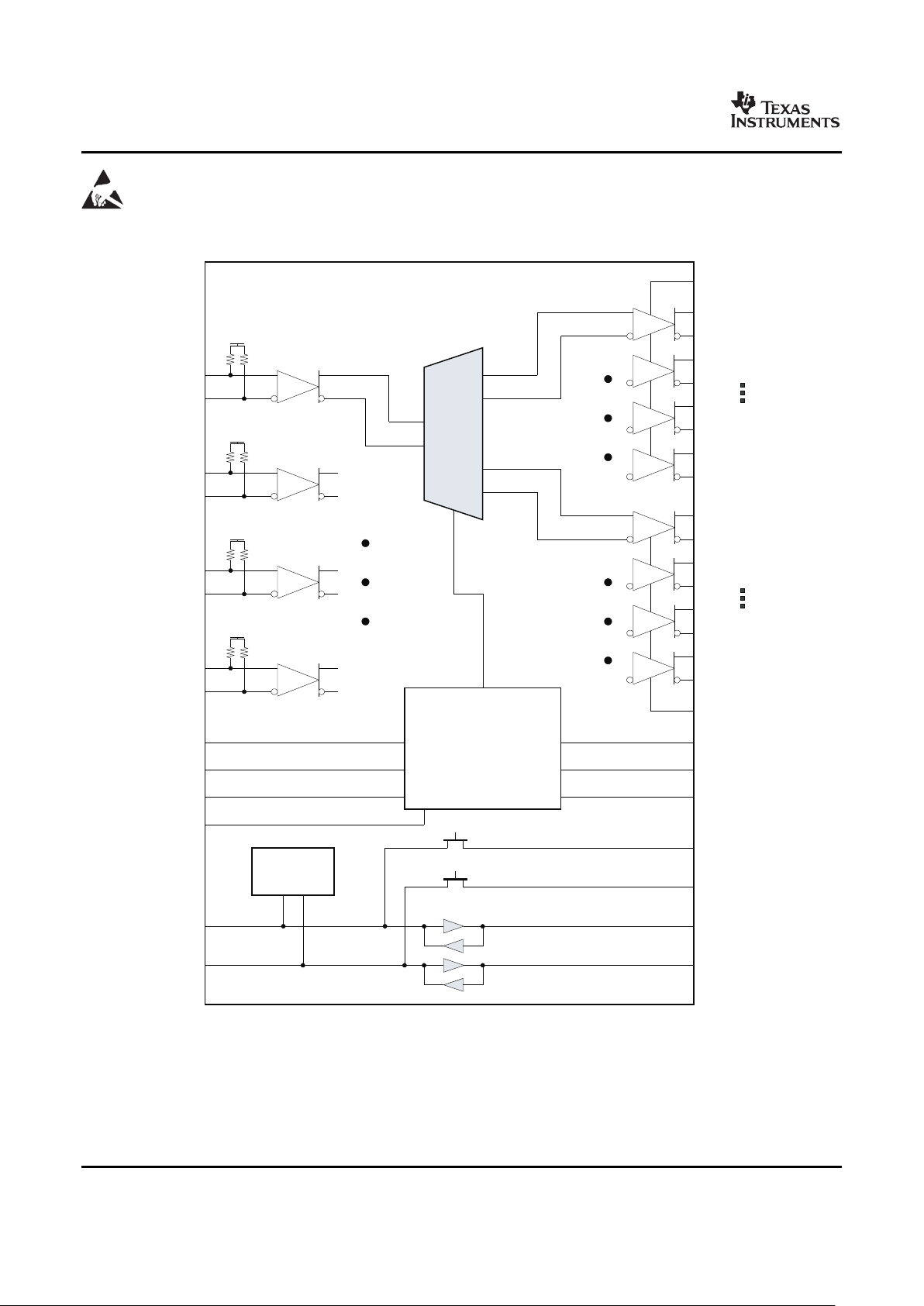
DATA FLOW BLOCK DIAGRAM
ML_IN 2(p)
ML_IN 2(n)
ML_IN 3(n)
ML_IN 3(p)
ML_IN 0(p)
ML_IN 0(n)
ML_IN 1(p)
ML_IN 1(n)
AUX(p)_I2C (SCL)
AUX(n)_I2C (SDA)
AUX_SINK (p)
AUX_SINK (n)
I2C_SCL
I2C_SDA
DP_SINK 0(n)
DP_SINK 0(p)
DP_SINK 3(p)
DP_SINK 3(n)
TMDS_SINK_CLK (p)
V
Sadj
Receiver
50 W
V
BIAS
I2C_SCL
I2C_SDA
TMDS_SINK_CLK (n)
TMDS_SINK 2(p)
TMDS_SINK 2(n)
Priority
DP_HPD_SINK
TMDS_HPD_SINK
HPD
CAD
CAD_SINK
Receiver
V
BIAS
Receiver
V
BIAS
Receiver
V
BIAS
Driver
Driver
Driver
Driver
Driver
Driver
Driver
Driver
2-to-1
MUX
Switching
Logic
I2CLogic
DP
Vadj
__
LP
50 W
50 W
50 W
50 W
50 W
50 W
50 W
SN75DP122
SLLS892 – FEBRUARY 2008
These devices have limited built-in ESD protection. The leads should be shorted together or the device placed in conductive foam
during storage or handling to prevent electrostatic damage to the MOS gates.
2 Submit Documentation Feedback Copyright © 2008, Texas Instruments Incorporated
Product Folder Link(s): SN75DP122
www.ti.com
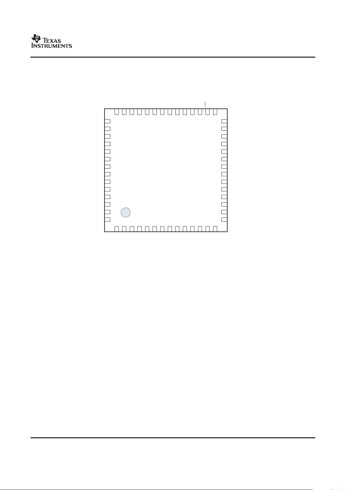
VCC
VDD
GND
GND
GND
VCC
1
24
23
22
21
20
19
18
17
16
15
14
13
12
11
10
9
8
76
5432
25
26
34
33
32
31
30
29
28
27
40 39
38
37
36
35
48
47
46
45
44
43
42 41
53
56
55
54
52
51
50
49
VDD
GND
VSadj
AUX_SINK(n)
AUX_SINK(p)
DP_SINK3(n)
DP_SINK3(p)
DP_SINK2(n)
DP_SINK2(p)
DP_SINK1(n)
DP_SINK1(p)
DP_SINK0(n)
DP_SINK0(p)
I2C_SDA
TMDS_SINK2(p)
TMDS_SINK2(n)
TMDS_SINK1(p)
TMDS_SINK1(n)
TMDS_SINK0(p)
TMDS_SINK0(n)
TMDS_SINKCLK(p)
TMDS_SINKCLK(n)
GND
CAD_SINK
DP_HPD_SINK
CAD
VDD
*
1
HPD
AUX(p)_I
2
C(SCL)
AUX(n)_I
2
C(SDA)
VDD
Priority
TMDS_HPD_SINK
I
2
C_EN
LP
I
2
C_SCL
DPVadj
VDD
ML_IN0(p)
ML_IN0(n)
GND
ML_IN1(p)
ML_IN1(n)
VDD
ML_IN2(p)
ML_IN2(n)
GND
ML_IN3(p)
ML_IN3(n)
VCC
SN75DP122
SN75DP122
SLLS892 – FEBRUARY 2008
Copyright © 2008, Texas Instruments Incorporated Submit Documentation Feedback 3
Product Folder Link(s): SN75DP122
www.ti.com
SN75DP122
SLLS892 – FEBRUARY 2008
TERMINAL FUNCTIONS
TERMINAL
I/O DESCRIPTION
NAME NO.
MAIN LINK INPUT PINS
ML_IN 0 3, 4 I DisplayPort main link channel 0 differential input
ML_IN 1 6, 7 I DisplayPort main link channel 1 differential input
ML_IN 2 9, 10 I DisplayPort main link channel 2 differential input
ML_IN 3 12, 13 I DisplayPort main link channel 3 differential input
MAIN LINK PORT A OUTPUT PINS
DP_SINK 0 56, 55 O DisplayPort main link port a channel 0 differential output
DP_SINK 1 53, 52 O DisplayPort main link port a channel 1 differential output
DP_SINK 2 50, 49 O DisplayPort main link port a channel 2 differential output
DP_SINK 3 47, 46 O DisplayPort main link port a channel 3 differential output
MAIN LINK PORT B OUTPUT PINS
TMDS_SINK 2 25, 24 O TMDS data 2 differential output
TMDS_SINK 1 22, 21 O TMDS data 1 differential output
TMDS_SINK 0 19, 18 O TMDS data 0 differential output
TMDS_SINK CLK 16, 15 O TMDS data clock differential output
HOT PLUG DETECT PINS
HPD 37 O Hot plug detect output to the displayport source
DP_HPD_SINK 40 I DisplayPort port hot plug detect input
TMDS_HPD_SINK 32 I TMDS port hot plug detect input
AUXILIARY DATA PINS
AUX_I
2
C 36, 35 I/O Source side bidirectional displayport auxiliary data line
AUX_SINK 45, 43 I/O DisplayPort port bidirectional displayport auxiliary data line
I2C_SCL 29,
I/O TMDS port bidirectional ddc data lines
I2C_SDA 28
CABLE ADAPTER DETECT PINS
CAD 39 O Cable adapter detect output to the displayport source
CAD_SINK 41 I DisplayPort cable adapter detect input
CONTROL PINS
LP 30 I Low power select bar
Priority 33 I Output port priority selection
DPVadj 1 I DisplayPort main link output gain adjustment
VSadj 26 I TMDS compliant voltage swing control
I2C_EN 31 I Internal I2C register enable, used for HDMI / DVI connector differentiation
SUPPLY and GROUND PINS
VDD 2, 8, 34, 48, 54 5-V supply
VDD
*1
38 HPD/CAD supply
VCC 14, 17, 23 3.3-V supply
GND 5, 11, 20, 27, 42, 44, 51 Ground
4 Submit Documentation Feedback Copyright © 2008, Texas Instruments Incorporated
Product Folder Link(s): SN75DP122
www.ti.com
ABSOLUTE MAXIMUM RATINGS
SN75DP122
SLLS892 – FEBRUARY 2008
Table 1. Control Pin Lookup Table
SIGNAL LEVEL
(1)
STATE DESCRIPTION
H Normal Mode Normal operational mode for device
LP
Device is forced into a low power state causing the outputs to go to a high impedance
L Low Power Mode
state. All other inputs are ignored
H TMDS Port has
If both DP_HPD_SINK and TMDS_HPD_SINK are high, the TMDS port is selected
Priority
Priority
L DP Port has Priority If both DP_HPD_SINK and TMDS_HPD_SINK are high, the DP port is selected
The Internal I2C register is active and readable when the TMDS port is selected
H HDMI
indicating that the connector being used is HDMI
I2C_EN
The Internal I2C register is disabled and not readable when the TMDS port is selected
L DVI
indicating that the connector being used is DVI
4.53 k Ω Increased Gain Main link displayport output has an increased voltage swing
DP
Vadj
6.49 k Ω Nominal Gain Main link displayport output has a nominal voltage swing
10 k Ω Decreased Gain Main link displayport output has a decreased voltage swing
Compliant Voltage
VS
adj
5.11 k Ω Driver output voltage swing precision control to aid with system compliance
Swing
(1) (H) Logic High; (L) Logic Low
Explanation of the internal switching logic of the SN75DP122 is located in the application section at the end of
this data sheet.
ORDERING INFORMATION
(1)
PART NUMBER PART MARKING PACKAGE
SN75DP122RTQR 75DP122 56-pin QFN Reel (large)
SN75DP122RTQT 75DP122 56-pin QFN Reel (small)
(1) For the most current package and ordering information, see the Package Option Addendum at the end of this document, or see the TI
web site at www.ti.com .
over operating free-air temperature range (unless otherwise noted)
(1)
VALUE UNIT
Supply voltage range
(2)
VDD, V
DD
*1
– 0.3 to 5.25 V
Supply voltage range V
CC
– 0.3 to 3.6 V
Main Link I/O (ML_IN x, DP_SINK x) Differential Voltage 1.5 V
TMDS I/O – 0.3 to 4 V
Voltage range HPD and CAD I/O – 0.3 to 5.25 V
Auxiliary I/O – 0.3 to 5.25 V
Control I/O – 0.3 to 5.25 V
Auxiliary and I2C I/O ± 8000
Human body model
(3)
V
All other pins ± 12000
Electrostatic discharge
Charged-device model
(3)
± 1000 V
Machine model
(4)
± 200 V
Continuous power dissipation See Dissipation Rating Table
(1) Stresses beyond those listed under absolute maximum ratings may cause permanent damage to the device. These are stress ratings
only and functional operation of the device at these or any conditions beyond those indicated under recommended operating conditions
is not implied. Exposure to absolute-maximum-rated conditions for extended periods may affect device reliability.
(2) All voltage values, except differential voltages, are with respect to network ground terminal.
(3) Tested in accordance with JEDEC Standard 22, Test Method A114-B
(4) Tested in accordance with JEDEC Standard 22, Test Method A115-A
Copyright © 2008, Texas Instruments Incorporated Submit Documentation Feedback 5
Product Folder Link(s): SN75DP122
www.ti.com
DISSIPATION RATINGS
THERMAL CHARACTERISTICS
RECOMMENDED OPERATING CONDITIONS
SN75DP122
SLLS892 – FEBRUARY 2008
PCB JEDEC DERATING FACTOR
(1)
TA= 85 ° C
PACKAGE TA< 25 ° C
STANDARD
ABOVE TA= 25 ° C POWER RATING
Low-K 3623 mW 36.23 mW/ ° C 1449 mW
56-Pin QFN (RTQ)
High-K 1109 mW 11.03 mW/ ° C 443.9 mW
(1) This is the inverse of the junction-to-ambient thermal resistance when board-mounted and with no air flow.
over operating free-air temperature range (unless otherwise noted)
PARAMETER TEST CONDITIONS MIN TYP MAX
(1)
UNIT
Junction-to-board thermal
R
θ JB
4x4 Thermal vias under powerpad 11.03 ° C/W
resistance
Junction-to-case thermal
R
θ JC
20.4 C/W
resistance
LP = 5 V, ML: VID= 600 mV, 2.7 Gbps PRBS;
Device power dissipation
P
D(1)
AUX: VID= 500 mV, 1 Mbps PRBS; 250 305 mW
DisplayPort selected
HPD/CAD = 5 V; V
DD
*1
= V
DD
LP = 5 V, ML: VID= 500 mV, 2.5 Gbps PRBS;
Device power dissipation TMDS
P
D(2)
270 420 mW
I2C: VID= 3.3 V, 100 Kbps PRBS; HPD/CAD = 5
selected
V; V
DD
*1
= V
DD
LP = 0 V, ML: VID= 600 mV, 2.7 Gbps PRBS;
Device power dissipation under
P
SD
75 85 µ W
AUX: VID= 500 mV, 1 Mbps PRBS; HPD/CAD =
low power
5 V; V
DD
*1
= V
DD
(1) The maximum rating is simulated under 5.25 V VDD.
MIN NOM MAX UNIT
V
DD
Supply voltage 4.5 5 5.25 V
V
DD
*1
HPD and CAD output reference voltage 1.62 5.25 V
V
CC
Supply voltage 3 3.3 3.6 V
T
A
Operating free-air temperature 0 85 ° C
MAIN LINK DIFFERENTIAL PINS
V
ID
Peak-to-peak input differential voltage 0.15 1.40 V
d
R
Data rate 2.7 Gbps
R
t
Termination resistance 45 50 55 Ω
V
Oterm
Output termination voltage 0 2 V
TMDS DIFFERENTIAL OUTPUT PINS
AV
CC
TMDS output termination voltage 3 3.3 3.6 V
d
R
Data rate 2.5 Gbps
R
t
Termination resistance 45 50 55 Ω
AUXILIARY AND I2C PINS
V
I
Input voltage 0 5.25 V
d
R(AUX)
Auxiliary data rate 1 MHz
d
R(I2C)
I2C data rate 100 kHz
HPD, CAD, AND CONTROL PINS
V
IH
High-level input voltage 2 5.25 V
V
IL
Low-level input voltage 0 0.8 V
6 Submit Documentation Feedback Copyright © 2008, Texas Instruments Incorporated
Product Folder Link(s): SN75DP122
www.ti.com
DEVICE POWER
ELECTRICAL CHARACTERISTICS
HOT PLUG AND CABLE ADAPTER DETECT
ELECTRICAL CHARACTERISTICS
SWITCHING CHARACTERISTICS
SN75DP122
SLLS892 – FEBRUARY 2008
The SN75DP122 is designed to operate off of two supply voltages. The DisplayPort port and the digital logic run
off of the 5V supply voltage. The TMDS level translator is powered off of the 3.3V supply.
over recommended operating conditions (unless otherwise noted)
PARAMETER TEST CONDITIONS MIN TYP MAX UNIT
I
DD
LP = 5 V, V
DD
*1
= VDD, Priority = 0 V 60 65
ML: VID= 600 mV, 2.7 Gbps PRBS
Supply current mA
AUX: VID= 500 mV, 1 Mbps PRBS
I
CC
0.1 0.25
DP/TMDS_HPD_SINK and CAD_SINK = 5 V
I
DD(2)
LP = 5 V, V
DD
*1
= VDD, Priority = 1 V 2 4
ML: VID= 500 mV, 2.5 Gbps PRBS
Supply current mA
AUX: VI= 2 V, 100 kHz
I
CC(2)
80 110
DP/TMDS_HPD_SINK and CAD_SINK = 5 V
I
DD
*1
Supply current V
DD
*1
= 5.25 V 0.1 4 mA
I
SD
Shutdown current LP = 0 V 1 16 µ A
The SN75DP122 is designed to support the switching of the Hot Plug Detect and Cable adapter Detect signals.
The SN75DP122 has a built in level shifter for the HPD and CAD outputs. The output voltage level of the HPD
and CAD pins is defined by the voltage level of the V
DD
*1
pin.
When the DisplayPort port is selected, the state of CAD_SINK is propagated to the CAD output pin. If the TMDS
port is selected, the CAD output pin stays HIGH as long as that port is selected.
Explanation of HPD and the internal logic of the SN75DP128 is located in the application section at the end of
the data sheet.
over recommended operating conditions (unless otherwise noted)
PARAMETER TEST CONDITIONS MIN TYP MAX UNIT
V
OH5
High-level output voltage IOH= – 100 µ A, V
DD
*1
= 5 V 4.5 5 V
V
OH3.3
High-level output voltage IOH= – 100 µ A, V
DD
*1
= 3.3 V 3 3.3 V
V
OH2.5
High-level output voltage IOH= – 100 µ A, V
DD
*1
= 2.5 V 2.25 2.5 V
V
OH1.8
High-level output voltage IOH= – 100 µ A, V
DD
*1
= 1.8 V 1.62 1.8 V
V
OL
Low-level output voltage IOH= 100 µ A, 0 0.4 V
I
H
High-level input current VIH= 2.0 V, V
DD
= 5.25 V – 10 10 µ A
I
L
Low-level input current VIL= 0.8 V, V
DD
= 5.25 V – 10 10 µ A
over recommended operating conditions (unless otherwise noted)
PARAMETER TEST CONDITIONS MIN TYP MAX UNIT
t
PD(CAD)
Propagation delay V
DD
*1
= 5 V 5 30 ns
t
PD(HPD)
Propagation delay V
DD
*1
= 5 V 30 110 ns
t
T1(HPD)
HPD logic switch pause time V
DD
*1
= 5 V 2 4.7 ms
t
T2(HPD)
HPD logic switch time V
DD
*1
= 5 V 170 400 ms
t
M(HPD)
Minimum output pulse duration V
DD
*1
= 5 V 100 ns
t
Z(HPD)
Low power to high-level propagation delay V
DD
*1
= 5 V 30 50 110 ns
Copyright © 2008, Texas Instruments Incorporated Submit Documentation Feedback 7
Product Folder Link(s): SN75DP122
www.ti.com
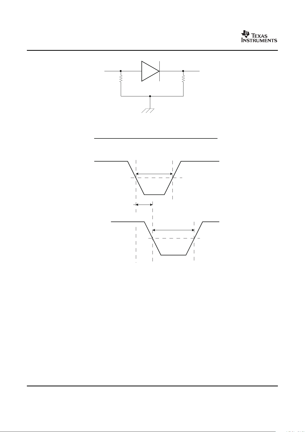
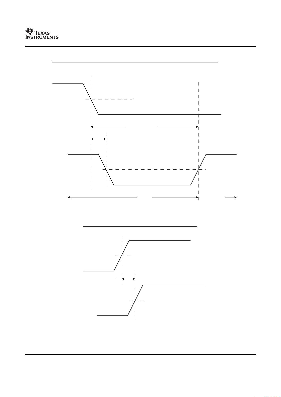
HPDInput
100kW
100kW
HPDOutput
DP122
SinkHotPlugDetect
PulseDuration
Minimum
HotPlugDetect
OutputPulseDuration
HPD
0V
V
DD
HPD_B
HPD_A
50%
t
PD(HPD)
V
DD
*1
0V
0V
50%
t
m(HPD)
SN75DP122
SLLS892 – FEBRUARY 2008
Figure 1. HPD Test Circuit
Figure 2. HPD Timing Diagram #1
8 Submit Documentation Feedback Copyright © 2008, Texas Instruments Incorporated
Product Folder Link(s): SN75DP122
www.ti.com
SinkHotPlugDetect
Timeout
PortB
Selected
Port A
Selected
HPD
Priority
HPD_A &HPD_B
V
DD
V
DD
50%
0V
V
DD
*1
t
1(HPD)
50%
t
2(HPD)
0V
HPD
0V
V
DD
0V
0V
V
DD
*1
50%
t
Z(HPD)
50%
HPD_B
HPD_A
SN75DP122
SLLS892 – FEBRUARY 2008
Figure 3. HPD Timing Diagram #2
Figure 4. HPD Timing Diagram #3
Copyright © 2008, Texas Instruments Incorporated Submit Documentation Feedback 9
Product Folder Link(s): SN75DP122
www.ti.com
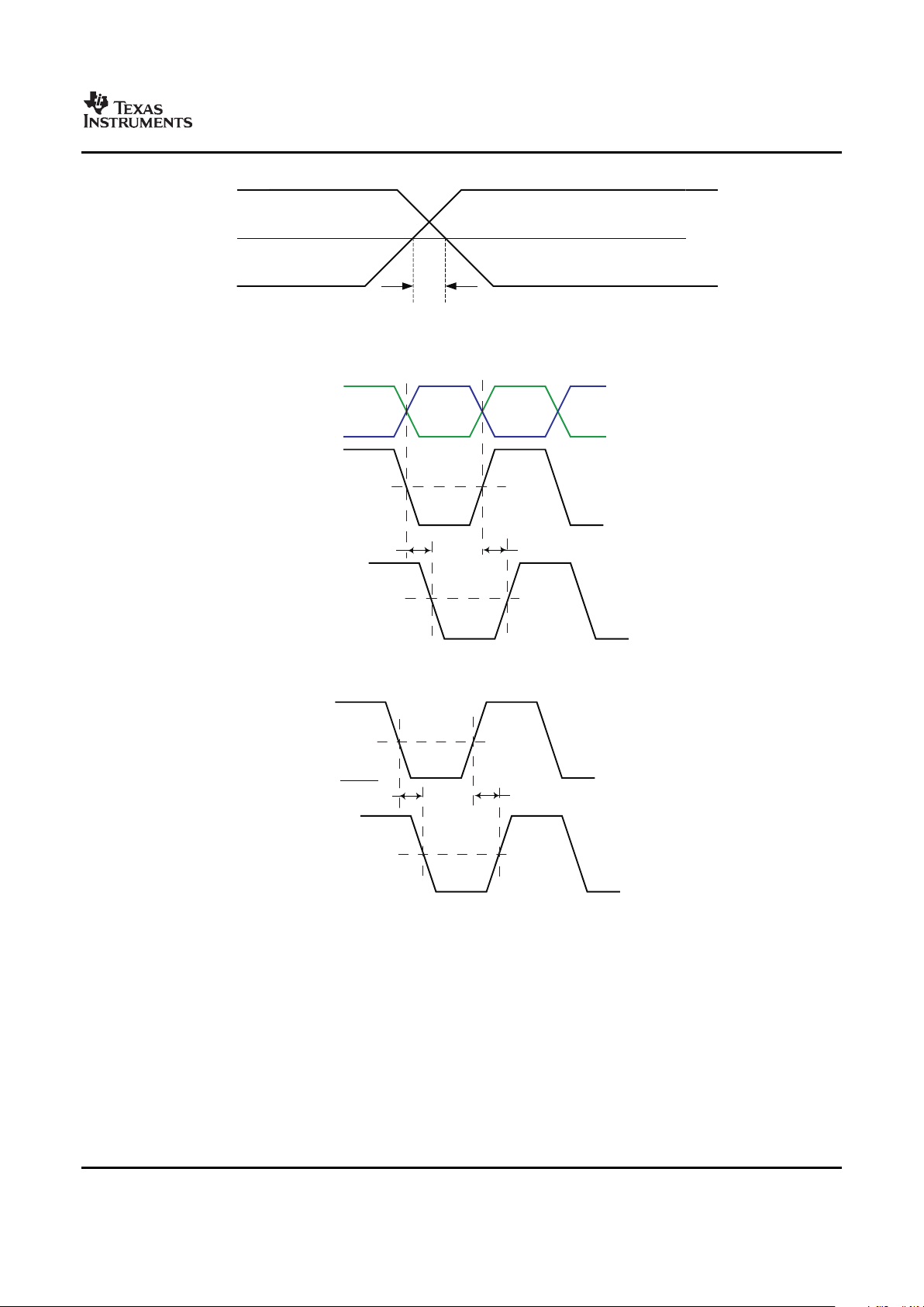
DisplayPort Auxiliary Pins
ELECTRICAL CHARACTERISTICS
SWITCHING CHARACTERISTICS
3.3V
10 pF
0.5 pF
AUX+
AUX-
50 W 50 W
100 W
SN75DP122
CAD=0
AUX
+ or -
3.3 V3.3 V
10 pF 50 pF
2kW
100kW
SN75DP122
CAD=1
SN75DP122
SLLS892 – FEBRUARY 2008
The SN75DP122 is designed to support the bidirectional auxiliary signals through the DisplayPort port in both a
differential (DisplayPort) mode and an I2C (DVI, HDMI) mode. The performance of the Auxiliary bus is optimized
based on the status of the CAD_SINK pin.
over recommended operating conditions (unless otherwise noted)
PARAMETER TEST CONDITIONS MIN TYP MAX UNIT
V
Pass1
Maximum passthrough voltage (CAD=1) V
DD
= 4.5 V, VI= 5 V, IO= 100 µ A 2.4 3.6 V
I
OZ
Output current from unselected output V
DD
= 5.25 V, VO= 0 V to 3.6 V, VI= 0 V – 5 5 µ A
DC bias = 1 V, AC = 1.4 V
p-p
, F = 100 kHz,
C
IO(off)
I/O capacitance when in low power 9 12 pF
CAD = High
DC bias = 1 V, AC = 1.4 V
p-p
, F = 100 kHz,
C
IO(on)
I/O capacitance when in normal operation 18 25 pF
CAD = Low
r
ON(C0)
On resistance V
DD
= 4.5 V, VI= 0 V or 3.6 V, IO= 5 mA, CAD = Low 5 10 Ω
Δ r
ON
On resistance V
DD
= 4.5 V, VI= 0 V or 2 V, IO= 5 mA, CAD = Low 1 5 Ω
V
DD
= 4.5 V, VI= 0 V or 3.6 V, IO= 5 mA, CAD =
r
ON(C1)
On resistance 10 18 Ω
High
over recommended operating conditions (unless otherwise noted)
PARAMETER TEST CONDITIONS MIN TYP MAX UNIT
t
sk(AUX)
Intra-pair skew VID= 400 mV, VIC= 2 V 40 80 ps
I
L(AUX)
Single Line Insertion Loss VID= 500 mV, VIC= 2 V, F = 1 MHz, CAD = Low 0.4 dB
t
PLH(AUXC0)
Propagation delay time, low to high CAD = Low, F = 1 MHz 3 ns
t
PHL(AUXC0)
Propagation delay time, high to low CAD = Low, F = 1 MHz 3 ns
t
PLH(AUXC1)
Propagation delay time, low to high CAD = High, F = 100 kHz 3 ns
t
PHL(AUXC1)
Propagation delay time, high to low CAD = High, F = 100 kHz 3 ns
Figure 5. Auxiliary Channel Test Circuit (CAD = LOW)
Figure 6. Auxiliary Channel Test Circuit (CAD = HIGH)
10 Submit Documentation Feedback Copyright © 2008, Texas Instruments Incorporated
Product Folder Link(s): SN75DP122
www.ti.com
50%
2.2V
1.8V
T
sk(AUX)
Differential
AUXInput
Differential
AUXOutput
AUXInput
2.2V
1.8V
0V
0V
t
PHL(AUXCO)
t
PLH(AUXCO)
AUX
Input
+ or -
AUX
Output
+ or -
2V
1V
1V
0V
2V
0V
t
PHL(AUXC1)
t
PLH(AUXC1)
DisplayPort Link Pins
SN75DP122
SLLS892 – FEBRUARY 2008
Figure 7. Auxiliary Channel Skew Measurement
Figure 8. Auxiliary Channel Delay Measurement (CAD = LOW)
Figure 9. Auxiliary Channel Delay Measurement (CAD = HIGH)
The SN75DP122 is designed to support DisplayPort ’ s high speed differential main link through the DisplayPort
port. The main link I/O of the SN75DP122 are designed to track the magnitude and frequency characteristics of
the input waveform and replicate them on the output. A feature has also been incorporated in the SN75DP122 to
increase the either increase of decrease the output amplitude via the resistor connected between the DPVADJ
pin and ground.
Copyright © 2008, Texas Instruments Incorporated Submit Documentation Feedback 11
Product Folder Link(s): SN75DP122

www.ti.com
ELECTRICAL CHARACTERISTICS
SWITCHING CHARACTERISTICS
Driver
V
Iterm
50 W
Receiver
D+
D-
V
D+
V
D-
V
ID
V
ICM
=(VD++ VD-)
0.5 pF
Y
Z
V
Y
V
Z
VOD= VY- V
Z
100 pF
100 pF
0Vto2V
VID= VD+- V
D-
2
VOC=(VY+ VZ)
2
50 W
50 W
50 W
Output
Input
DV
I/O
InputEdgeRate
20%to80%
80ps
t
R/FDP
DV
I/O
SN75DP122
SLLS892 – FEBRUARY 2008
over recommended operating conditions (unless otherwise noted)
PARAMETER TEST CONDITIONS MIN TYP MAX UNIT
Δ V
I/O(2)
VID= 200 mV, DPV
adj
= 4.65 k Ω 0 30 60 mV
Δ V
I/O(3)
VID= 300 mV, DPV
adj
= 4.65 k Ω – 24 33 36 mV
Difference between input and output) voltages
(V
OD
– VID)
Δ V
I/O(4)
VID= 400 mV, DPV
adj
= 4.65 k Ω – 45 – 15 15 mV
Δ V
I/O(6)
VID= 600 mV, DPV
adj
= 4.65 k Ω – 87 – 47 – 22 mV
R
INT
Input termination impedance 45 50 55 Ω
V
Iterm
Input termination voltage 0 2 V
over recommended operating conditions (unless otherwise noted)
PARAMETER TEST CONDITIONS MIN TYP MAX UNIT
t
R/F(DP)
Output edge rate (20% – 80%) Input edge rate = 80 ps (20% – 80%) 115 160 ps
t
PD
Propagation delay time F= 1 MHz, VID= 400 mV 227 ps
t
SK(1)
Intra-pair skew F= 1 MHz, VID= 400 mV 20 ps
t
SK(2)
Inter-pair skew F= 1 MHz, VID= 400 mV 40 ps
t
DPJIT(PP)
Peak-to-peak output residual jitter dR= 2.7 Gbps, VID= 400 mV, PRBS 27-1 25 35 ps
Figure 10. Main Link Test Circuit
Figure 11. Main Link Δ V
I/O
and Edge Rate Measurements
12 Submit Documentation Feedback Copyright © 2008, Texas Instruments Incorporated
Product Folder Link(s): SN75DP122

www.ti.com
MainLink
Input
MainLink
Output
ML_INx+
ML_INx-
0V
0V
t
PD(ML)
t
PD(ML)
ML x+
ML x-
ML y+
ML y-
2.2V
1.8V
2.2V
1.8V
50%
50%
T
sk1
T
sk2
T
sk1
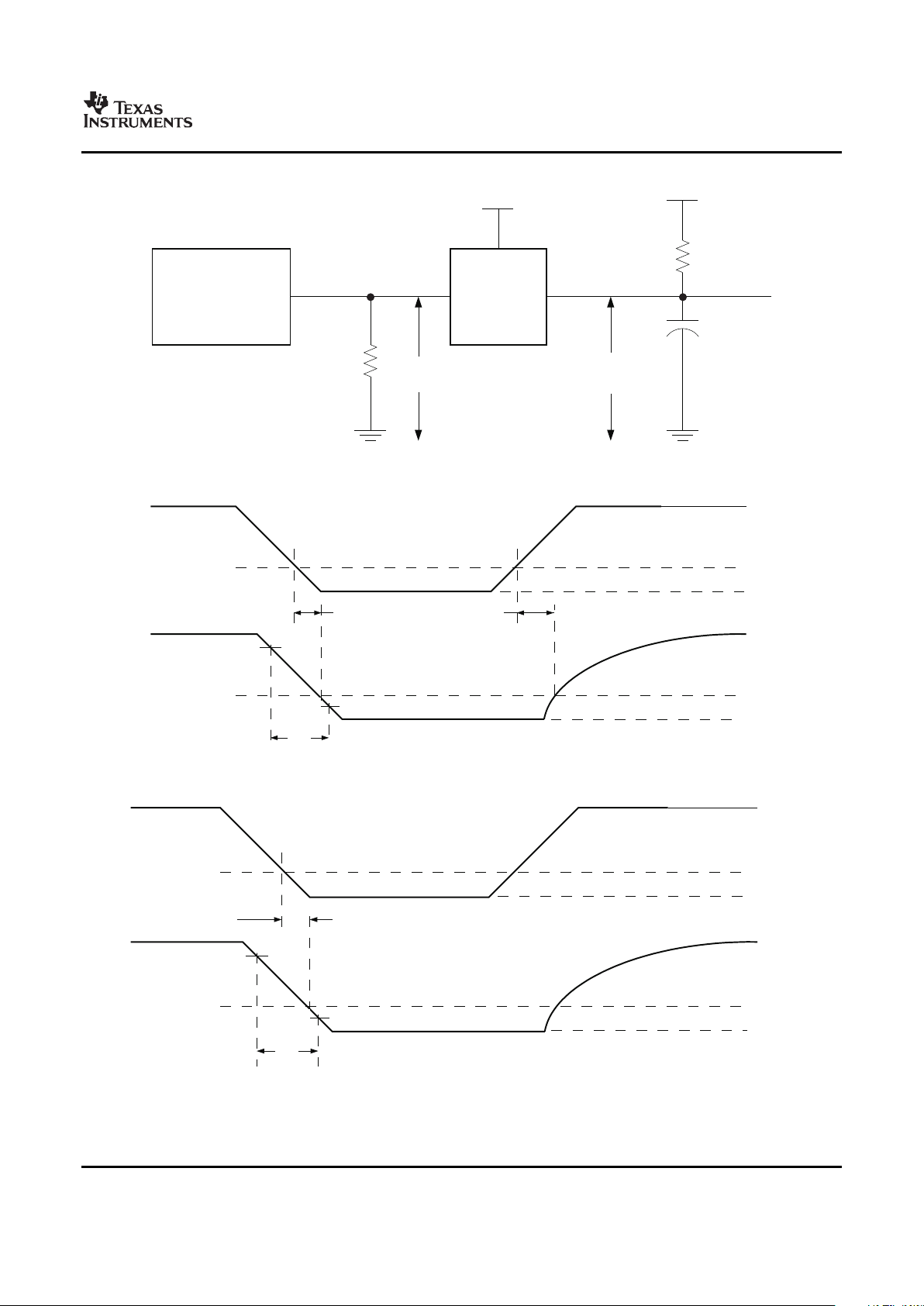
TMDS I2C Pins
ELECTRICAL CHARACTERISTICS
SN75DP122
SLLS892 – FEBRUARY 2008
Figure 12. Main Link Delay Measurements
Figure 13. Main Link Skew Measurements
When the TMDS port is selected the SN75DP122 utilizes an I2C repeater. The repeater is designed to isolate the
parasitic effects of the system in order to aid with system level compliance.
In addition to the I2C repeater, the SN75DP122 also supports the connector detection I2C register. This register
is enabled via the I2C_EN pin. When active an internal memory register is readable via the AUX_I
2
C I/O. The
functionality of this register block is described in the application section
over recommended operating conditions (unless otherwise noted)
PARAMETER TEST CONDITIONS MIN TYP MAX UNIT
I
OH
High output current VO= 5.25 V 10 µ A
I
L
Low input current V
CC
= 3.6 V, VI= 0 V 10 µ A
I
lkg(AUX)
Input leakage AUX_I
2
C pins V
CC
= 3.6 V, VI= 2 V – 10 10 µ A
Copyright © 2008, Texas Instruments Incorporated Submit Documentation Feedback 13
Product Folder Link(s): SN75DP122

www.ti.com
SWITCHING CHARACTERISTICS
PULSE
GENERATOR
R
T
V
IN
V
OUT
V
CC
D.U.T.
3.3V
R =2kLW
C
L
=100pF
SN75DP122
SLLS892 – FEBRUARY 2008
ELECTRICAL CHARACTERISTICS (continued)
over recommended operating conditions (unless otherwise noted)
PARAMETER TEST CONDITIONS MIN TYP MAX UNIT
Input/output capacitance DC bias = 1 V, AC = 1.4 V
p-p
,
C
IO(AUX)
AUX_I
2
C pins 15 pF
f = 100 kHz
V
IH(AUX)
High-level input voltage AUX_I
2
C pins 1.6 2 V
V
IL(AUX)
Low-level input voltage AUX_I
2
C pins – 0.2 0.4 V
V
OL(AUX)
Low-level output voltage AUX_I
2
C pins IO= 4 mA 0.5 0.6 V
I
lkg(I2C)
Input leakage current I2C SDA/SCL pins V
CC
= 3.6 V, VI= 5.25 V – 10 10 µ A
DC bias = 2.5 V,
C
IO(I2C)
Input/output capacitance I2C SDA/SCL pins 15 pF
AC = 3.5 V
p-p
, f = 100 kHz
V
IH(I2C)
High-level input voltage I2C SDA/SCL pins 2.1 5.25 V
V
IL(I2C)
Low-level input voltage I2C SDA/SCL pins -0.2 1.5 V
V
OL(I2C)
Low-level output voltage I2C SDA/SCL pins IO = 4 mA 0.2 V
over recommended operating conditions (unless otherwise noted)
PARAMETER TEST CONDITIONS MIN TYP MAX UNIT
t
PLH1
Propagation delay time, low to high Source to sink 204 459 ns
t
PHL1
Propagation delay time, high to low Source to sink 35 140 ns
t
PLH2
Propagation delay time, low to high Sink to source 80 251 ns
t
PHL2
Propagation delay time, high to low Sink to source 35 200 ns
t
f1
Output signal fall time Sink side 20 72 ns
t
f2
Output signal fall time Source side 20 72 ns
f
SCL
SCL clock frequency for internal register Source side 100 kHz
t
W(L)
Clock LOW period for I2C register Source side 4.7 µ s
t
W(H)
Clock HIGH period for internal register Source side 4.0 µ s
t
SU1
Internal register setup time, SDA to SCL Source side 250 ns
t
h(1)
Internal register hold time, SCL to SDA Source side 0 µ s
T
(buf)
Internal register bus free time between STOP and START Source side 4.7 µ s
t
su(2)
Internal register setup time, SCL to START Source side 4.7 µ s
t
h(2)
Internal register hold time, START to SCL Source side 4.0 µ s
t
su(3)
Internal register hold time, SCL to STOP Source side 4.0 µ s
Figure 14. Source Side Test Circuit (AUX_I
2
C)
14 Submit Documentation Feedback Copyright © 2008, Texas Instruments Incorporated
Product Folder Link(s): SN75DP122
www.ti.com
PULS
GENERATOR
V
CC
5V
D.U.T.
R
T
V
IN
V
OUT
R =2kLW
C =400pF
L
I2C_SCL/
I2C_SDA
Input
AUX_I2C(p)/
AUX_I2C(n)
Output
t
PHL2
t
PLH2
80%
20%
t
f1
5V
1.6V
0.1V
3.3V
1.6V
V
OL
20%
I2C_SCL/
I2C_SDA
Output
AUX_I2C(p)/
AUX_I2C(n)
Input
t
PHL1
80%
t
f1
5V
1.6V
0.1V
3.3V
1.6V
V
OL
SN75DP122
SLLS892 – FEBRUARY 2008
Figure 15. Sink Side Test Circuit (SCL, SDA)
Figure 16. Source Side Output AC Measurements
Figure 17. Sink Side Output AC Measurements
Copyright © 2008, Texas Instruments Incorporated Submit Documentation Feedback 15
Product Folder Link(s): SN75DP122

www.ti.com
I2C_SCL/
I2C_SDA
Output
AUX_I2C(p)/
AUX_I2C(n)
Input
t
PHL1
0.5V
3.3V
1.6V
5V
TMDS MAIN LINK PINS
ELECTRICAL CHARACTERISTICS
SWITCHING CHARACTERISTICS
SN75DP122
SLLS892 – FEBRUARY 2008
Figure 18. Sink Side Output AC Measurements Continued
The TMDS port of the SN75DP122 is designed to be compliant with the Digital Video Interface (DVI) 1.0 and
High Definition Multimedia Interface (HDMI) 1.3 specifications. The differential output voltage swing can be fine
tuned with the VSadj resistor.
over recommended operating conditions (unless otherwise noted)
PARAMETER TEST CONDITIONS MIN TYP MAX UNIT
V
OH
Single-ended HIGH level output voltage AVCC – 10 AVCC+10 mV
V
OL
Single-ended LOW level output voltage AVCC – 600 AVCC – 400 mV
V
SWING
Single-ended output voltage swing 400 600 mV
AVCC = 3.3 V, RT= 50 Ω
Change in steady-state common-mode output
V
OC(SS)
– 5 5 mV
voltage between logic states
V
OD(PP)
Peak-to-Peak output differential voltage 800 1200 mV
AVCC = 3.3 V, RT= 50 Ω ,
V
(O)SBY
Single-ended standby output voltage AVCC – 10 AVCC+10 mV
DP Port Selected
0 V ≤ VCC ≥ 1.5 V,
I
(O)OFF
Single-ended power down output current – 10 10 µ A
AVCC = 3.3 V, RT= 50 Ω
I
OS
Short circuit output current VID = 500 mV – 15 15 mA
over recommended operating conditions (unless otherwise noted)
PARAMETER TEST CONDITIONS MIN TYP MAX UNIT
t
PLH
Propagation delay time 250 480 600 ps
t
PHL
Propagation delay time 250 400 800 ps
t
R
Rise time 60 90 140 ps
t
F
Fall time AVCC = 3.3 V, RT= 50 Ω , f = 1 MHz 60 90 140 ps
t
SK(P)
Pulse skew 8 15 ps
t
SK(D)
Intra-pair skew 20 40 ps
t
SK(O)
Inter-pair skew 20 65 ps
t
JITD(PP)
Peak-to-peak output residual data jitter AVCC = 3.3 V, RT= 50 Ω , dR = 2.5 Gbps 20 50 ps
t
JITC(PP)
Peak-to-peak output residual clock jitter AVCC = 3.3 V, RT= 50 Ω , f = 250 MHz 10 30 ps
16 Submit Documentation Feedback Copyright © 2008, Texas Instruments Incorporated
Product Folder Link(s): SN75DP122

www.ti.com
Driver
V
TERM
50 W
Receiver
3.3 V
D+
D-
V
D+
V
D-
V
ID
VID= VD+- V
D-
0.5 pF
Y
Z
V
Y
V
Z
VOD= VY- V
Z
V
ICM
=(VD++ VD-)
2
VOC=(VY+ VZ)
2
100 pF
100 pF
50 W
50 W
50 W
V
TERM
V
ID+
0V
V
ID
V
ID(pp)
t
PHL
t
PLH
80%
80%
0V
20% 20%
V
OD(pp)
V
OD
t
f
t
r
2.2V
1.8V
V
ID
V
OC
DV
OC(SS)
SN75DP122
SLLS892 – FEBRUARY 2008
Figure 19. TMDS Main Link Test Circuit
Figure 20. TMDS Main Link Timing Measurements
Figure 21. TMDS Main Link Common Mode Measurements
Copyright © 2008, Texas Instruments Incorporated Submit Documentation Feedback 17
Product Folder Link(s): SN75DP122

www.ti.com
Data+
Data-
Clk+
Clk-
Video
Patterm
Generator
1000 mVpp
Differential
Coax
Coax
Coax
Coax
Coax
Coax
Coax
Coax
SN75DP122
SMA
SMA
SMA
SMA
(4)
R
T
R
T
(5)
AVcc
R
T
R
T
Jitter Test
Instrument
(2,3)
TTP 4
TTP 2TTP 1
FR4 PCBtrace
(1)
&
ACcouplingCaps
FR4 PCBtrace
RX
+EQ
OUT
RX
+EQ
OUT
SMA
SMA
SMA
SMA
TTP 3
Jitter Test
Instrument
(2,3)
A
VCC
Driver
50 W
+
-
50 W
I
OS
0Vor3.6V
SN75DP122
SLLS892 – FEBRUARY 2008
(1) The FR4 trace between TTP1 and TTP2 is designed to emulate 8" of FR4, a connector, and another 8" of FR4.
(2) All Jitter is measured at a BER of 10
– 12
(3) Residual jitter reflects the total jitter measured at TTP4 minus the jitter measured at TTP1
(4) AVCC = 3.3 V
(5) RT= 50 Ω
Figure 22. TMDS Jitter Measurements
Figure 23. TMDS Main Link Short Circuit Output Circuit
18 Submit Documentation Feedback Copyright © 2008, Texas Instruments Incorporated
Product Folder Link(s): SN75DP122

www.ti.com
TYPICAL CHARACTERISTICS
−60
−50
−30
0
30
40
V − DifferentialVoltageDD− V
DV − Input/OutputVoltage − mV
I\O
4.4 5 5.14.5 4.7 4.8 4.9 5.2
V =300mV
ID
V =400mV
ID
−10
−40
−20
10
20
4.6 5.45.3
V =600mV
ID
Temp=25 C
o
V =200mV
ID
−150
−100
−50
0
50
100
150
DP − Resistance
Vadj
− W
D
V
− Input/OutputV
oltage − mV
I\O
0 10k 12k2k 4k 6k 8k 14k
V =200mV
ID
V =300mV
ID
V =400mV
ID
V =600mV
ID
Temp=25 C
o
200
300
400
500
DataRate − Bps
PowerDissipation − mW
0 2G 2.5G500M 1G 1.5G 3G
450
350
250
TMDS
DisplayPort
0
60
80
100
180
200
InputRiseTime20%-80%(ps)
OutputRiseTime20%-80%(ps)
0 140 16040 60 80 100 180
V =5.25V
DD
12020
V =4.5V
DD
V =5V
DD
40
20
140
120
160
SN75DP122
SLLS892 – FEBRUARY 2008
INPUT/OUTPUT VOLTAGE INPUT/OUTPUT VOLTAGE
vs vs
DP
Vadj
RESISTANCE SUPPLY VOLTAGE
Figure 24. Figure 25.
OUTPUT RISE TIME POWER DISSIPATION
vs vs
INPUT RISE TIME DATA RATE
Figure 26.
(1) TMDS power dissipation in this graph includes
132 mW of power supplied by the AVCC
termination.
Figure 27.
Copyright © 2008, Texas Instruments Incorporated Submit Documentation Feedback 19
Product Folder Link(s): SN75DP122

www.ti.com
0
15
25
DataRate − Bps
2G 2.5G500M 1G 1.5G 3G
20
10
5
Peak-PeakResidualDataJitter(ps)
V =400mV
ID
V =600mV
ID
V =500mV
ID
5
6
8
11
12
13
15
V SupplyVoltageCC− V−
2.7 3.63 3.3 3.9
14
10
9
7
Peak-PeakResidualDataJitter(ps)
25 C
o
85 C
o
0 C
o
0
400
800
1000
1400
VS
adj
− Resistance − W
6.5k6k4k 5k 7k
1200
600
200
V − − mV
OD
DifferentialOutputVoltage
3k 3.5k 4.5k 5.5k
3.6V,V
CC
3V,V
CC
3.3V,V
CC
SN75DP122
SLLS892 – FEBRUARY 2008
TYPICAL CHARACTERISTICS (continued)
TMDS PORT SUPPLY VOLTAGE TMDS PORT JITTER
vs vs
RESIDUAL DATA JITTER DATA RATE
Figure 28. Figure 29.
TMDS OUTPUT DIFFERENTIAL VOLTAGE
vs
VS
adj
RESISTANCE
Figure 30.
20 Submit Documentation Feedback Copyright © 2008, Texas Instruments Incorporated
Product Folder Link(s): SN75DP122

www.ti.com
APPLICATION INFORMATION
SWITCHING LOGIC
I2C INTERFACE NOTES
SDA
SCL
SDA
SCL
Start
Condition
Stop
Condition
GENERAL I2C PROTOCOL
SN75DP122
SLLS892 – FEBRUARY 2008
The Switching logic of the SN75DP122 is tied to the state of the HPD pins as well as the LP and priority pins.
When both HPD_A and HPD_B input pins are LOW, the SN75DP122 enters the low power state. In this state the
outputs are high impedance. When either HPD_A or HPD_B goes high, the device enters the normal operational
state and the port associated with the HPD pin that went high is selected. If both HPD_A and HPD_B are HIGH,
the port selection is determined by the state of the priority pin.
In order to ease the transitioning from one output port to the other output port the SN75DP122 forces the HPD
output pin LOW for an extended duration. This forced Low is designed to mimic an unplug event for the
transmitting device. This should allow for a smooth transition from one port to another. This forced LOW timer
can be bypassed by pulsing the LP pin LOW for a short duration and then returning to HIGH. When the LP pin if
driven LOW the device enters a low power state and the internal logic block is reset.
The I2C interface can be used to access the internal memory of the SN75DP122. I2C is a two-wire serial
interface developed by Philips Semiconductor (see I2C-Bus Specification, Version 2.1, January 2000). The bus
consists of a data line (SDA) and a clock line (SCL) with pull-up structures. When the bus is idle, both SDA and
SCL lines are pulled high. All the I2C compatible devices connect to the I2C bus through open drain I/O pins,
SDA and SCL. A master device, usually a microcontroller or a digital signal processor, controls the bus. The
master is responsible for generating the SCL signal and device addresses. The master also generates specific
conditions that indicate the START and STOP of data transfer. A slave device receives and/or transmits data on
the bus under control of the master device. The SN75DP122 works as a slave and supports the standard mode
transfer (100 kbps) and fast mode transfer (400 kbps) as defined in the I2C-Bus Specification.
The basic I2C start and stop access cycles are shown in Figure 31 .
The basic access cycle consists of the following:
• A start condition
• A slave address cycle
• Any number of data cycles
• A stop condition
Figure 31. I2C Start and Stop Conditions
• The master initiates data transfer by generating a start condition. The start condition is when a high-to-low
transition occurs on the SDA line while SCL is high, as shown in Figure 31 . All I2C-compatible devices should
recognize a start condition.
• The master then generates the SCL pulses and transmits the 7-bit address and the read/write direction bit
R/W on the SDA line. During all transmissions, the master ensures that data is valid. A valid data condition
requires the SDA line to be stable during the entire high period of the clock pulse (see Figure 32 ). All devices
recognize the address sent by the master and compare it to their internal fixed addresses. Only the slave
device with a matching address generates an acknowledge (see Figure 33 ) by pulling the SDA line low during
the entire high period of the ninth SCL cycle. On detecting this acknowledge, the master knows that a
Copyright © 2008, Texas Instruments Incorporated Submit Documentation Feedback 21
Product Folder Link(s): SN75DP122

www.ti.com
SDA
SCL
DataLine
Stable;
DataValid
ChangeofData Allowed
DataOutput
byTransmitter
DataOutput
byReceiver
SCL From
Master
START
Condition
ClockPulsefor
Acknowledgement
Not Acknowledge
Acknowledge
SCL
SDA
MSB
Acknowledge
Acknowledge
Stop
Slave Address
Data
SN75DP122
SLLS892 – FEBRUARY 2008
communication link with a slave has been established.
• The master generates further SCL cycles to either transmit data to the slave (R/W bit 0) or receive data from
the slave (R/W bit 1). In either case, the receiver needs to acknowledge the data sent by the transmitter. So
an acknowledge signal can either be generated by the master or by the slave, depending on which one is the
receiver. The 9-bit valid data sequences consisting of 8-bit data and 1-bit acknowledge can continue as long
as necessary (see Figure 34 ).
• To signal the end of the data transfer, the master generates a stop condition by pulling the SDA line from low
to high while the SCL line is high (see Figure 31 ). This releases the bus and stops the communication link
with the addressed slave. All I2C compatible devices must recognize the stop condition. Upon the receipt of a
stop condition, all devices know that the bus is released, and they wait for a start condition followed by a
matching address.
Figure 32. I2C Bit Transfer
Figure 33. I2C Acknowledge
Figure 34. I2C Address and Data Cycles
During a read cycle, the slave receiver acknowledges the initial address byte if it decodes the address as its
22 Submit Documentation Feedback Copyright © 2008, Texas Instruments Incorporated
Product Folder Link(s): SN75DP122

www.ti.com
SDA
I2CDevice Addressand
Read/WriteBit
FirstData
Byte
Other
DataBytes
LastDataByte
Stop
Condition
Start
Condition
Acknowledge
(From
Receiver)
Acknowledge
(From
Transmitter)
Not
Acknowledge
(Transmitter)
Slave Address
Sink Port Selection Register and Source Plug-In Status Register Description (Sub-Address)
SN75DP122
SLLS892 – FEBRUARY 2008
address. Following this initial acknowledge by the slave, the master device becomes a receiver and
acknowledges data bytes sent by the slave. When the master has received all of the requested data bytes from
the slave, the not acknowledge (A) condition is initiated by the master by keeping the SDA signal high just before
it asserts the stop (P) condition. This sequence terminates a read cycle as shown in Figure 35 and Figure 36 .
See Example – Reading from the SN75DP122 section for more information.
Figure 35. I2C Read Cycle
Figure 36. Multiple Byte Read Transfer
Both SDA and SCL must be connected to a positive supply voltage via a pull-up resistor. These resistors should
comply with the I2C specification that ranges from 2 k Ω to 19 k Ω . When the bus is free, both lines are high. The
address byte is the first byte received following the START condition from the master device. The 7-bit address is
factory preset to 1000000. Table 2 lists the calls that the SN75DP122 responds to.
Table 2. SN75DP122 Slave Address
FIXED ADDRESS READ/WRITE BIT
Bit 7 Bit 6 Bit 5 Bit 4 Bit 3 Bit 2 Bit 1 Bit 0
(MSB) (R/W)
1 0 0 0 0 0 0 1
The SN75DP122 operates using a multiple byte transfer protocol similar to Figure 36 . The internal memory of the
SN75DP122 contains the phrase DP-HDMI ADAPTOR<EOT> converted to ASCII characters. The internal
memory address registers and the value of each can be found in Table 3 .
During a read cycle, the SN75DP122 sends the data in its selected sub-address in a single transfer to the master
device requesting the information. See the Example – Reading from the SN75DP122 section of this document
for the proper procedure on reading from the SN75DP122.
Table 3. SN75DP122 Sink Port and Source Plug-In Status Registers Selection
Address 0x00 0x01 0x02 0x03 0x04 0x05 0x06 0x07 0x08 0x09 0x0A 0x0B 0x0C 0x0D 0x0E 0x0F 0x10
Data 44 50 2D 48 44 4D 49 20 41 44 41 50 54 4F 52 04 FF
Copyright © 2008, Texas Instruments Incorporated Submit Documentation Feedback 23
Product Folder Link(s): SN75DP122

www.ti.com
EXAMPLE – READING FROM THE SN75DP122
SN75DP122 Read Phase:
SWITCHING LOGIC
SN75DP122
SLLS892 – FEBRUARY 2008
The read operation consists of several steps. The I2C master begins the communication with the transmission of
the start sequence followed by the slave address of the SN75DP122. The SN75DP122 acknowledges its
presence to the master and begin to transmit the contents of the memory registers. After each byte is transferred
the SN75DP122 waits for either an acknowledge (ACK) or a not-acknowledge (NACK) from the master. If an
ACK is received, the next byte of data is transmitted. If a NACK is received the data transmission sequence is
expected to end and the master should send the stop command.
The SN75DP122 continues to send data as long as the master continues to acknowledge each byte
transmission. If an ACK is received after the transmission of byte 0x0F, the SN75DP122 transmits byte 0x10 and
continue to transmit byte 0x10 for all further ACK ’ s until a NACK is received.
Step 1 0
I2C Start (Master) S
Step 2 7 6 5 4 3 2 1 0
I2C General Address (Master) 1 0 0 0 0 0 0 1
Step 3 9
I2C Acknowledge (Slave) A
Step 10 7 6 5 4 3 2 1 0
I2C Read Data (Slave) Data Data Data Data Data Data Data Data
Where Data is determined by the logic values contained in the Sink port register
Step 11 9
I2C Not-Acknowledge (Master) X
Where X is either an A (Acknowledge) or A (Not-Acknowledge)
An A causes the pointer to increment and step 10 is repeated
An A causes the slave to stop transmitting and proceed to step 12
Step 12 0
I2C Stop (Master) P
The switching logic of the SN75DP122 is tied to the state of the HPD input pins as well as the priority pin and low
power pin. When both HPD_A and HPD_B input pins are LOW, the SN75DP122 enters the low power state. In
this state the outputs are high impedance, and the device is shutdown to optimize power conservation. When
either HPD_A or HPD_B goes high, the device enters the normal operational state, and the port associated with
the HPD pin that went high is selected. If both HPD_A and HPD_B are HIGH, the port selection is determined by
the state of the priority pin.
Several key factors were taken into consideration with this digital logic implementation of channel selection as
well as HPD repeating. This logic has been divided into the following four scenarios.
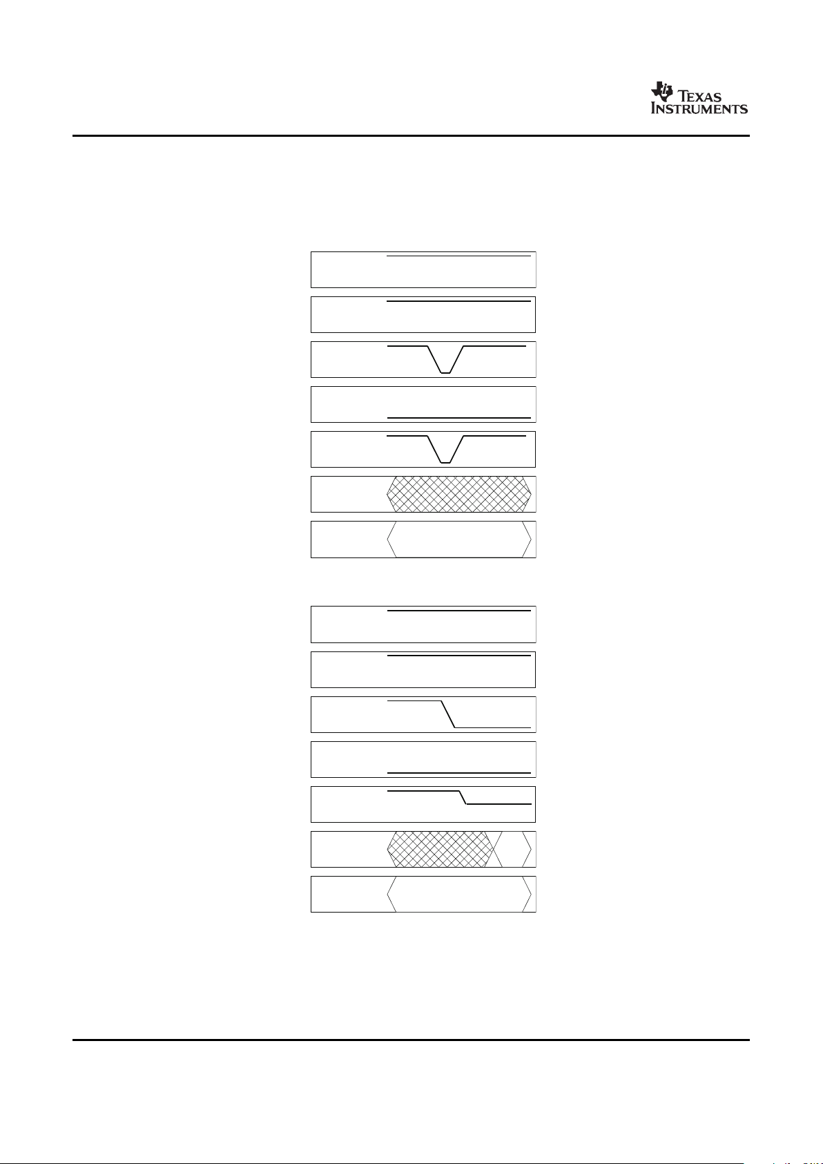
1. Low power state to active state. There are two possible cases for this scenario depending on the state of the
low power pin:
– Case one: In this case both HPD inputs are initially LOW and the low power pin is also LOW. In this initial
state the device is in a low power mode. Once one of the HPD inputs goes to a HIGH state, the device
remains in the low power mode with both the main link and auxiliary I/O in a high impedance state.
However, the port associated with the HPD input that went HIGH is still selected and the HPD output to
the source is enabled and follows the logic state of the input HPD (see Figure 37 ). The state of the
Priority pin has no effect in this scenario as only one HPD input port is active.
24 Submit Documentation Feedback Copyright © 2008, Texas Instruments Incorporated
Product Folder Link(s): SN75DP122

www.ti.com
LP
Priority
HPD_A
0
1
0
1
0
1
HPD_B
0
1
HPD_OUT
0
1
Channel A
Z
0
1
ChannelB
0
1
HI-Z
HI-Z
LP
Priority
HPD_A
0
1
0
1
0
1
HPD_B
0
1
HPD_OUT
0
1
Channel A
Z
0
1
ChannelB
0
1
HI-Z
HI-Z
DATA
SN75DP122
SLLS892 – FEBRUARY 2008
Figure 37.
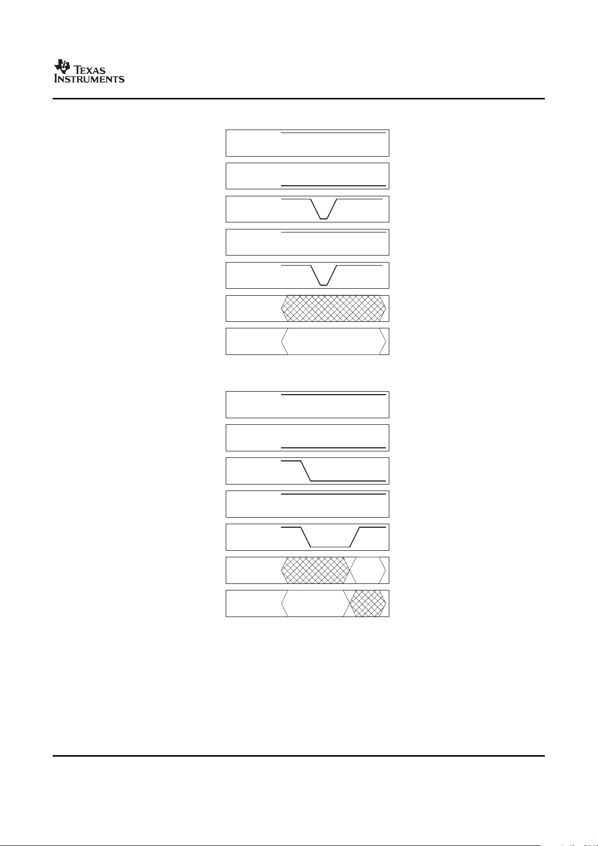
– Case two: In this case both HPD inputs are initially LOW and the low power pin is HIGH. In this initial
state the device is in a low power mode. Once one of the HPD inputs goes to a HIGH state, the device
comes out of the low power mode and enters active mode enabling the main link and auxiliary I/O. The
port associated with the HPD input that went HIGH is selected and the HPD output to the source is
enabled and follows the logic state of the input HPD (see Figure 38 ). This is specified as t
Z(HPD)
. Again,
the state of the Priority pin has no effect in this scenario as only one HPD input port is active.
Figure 38.
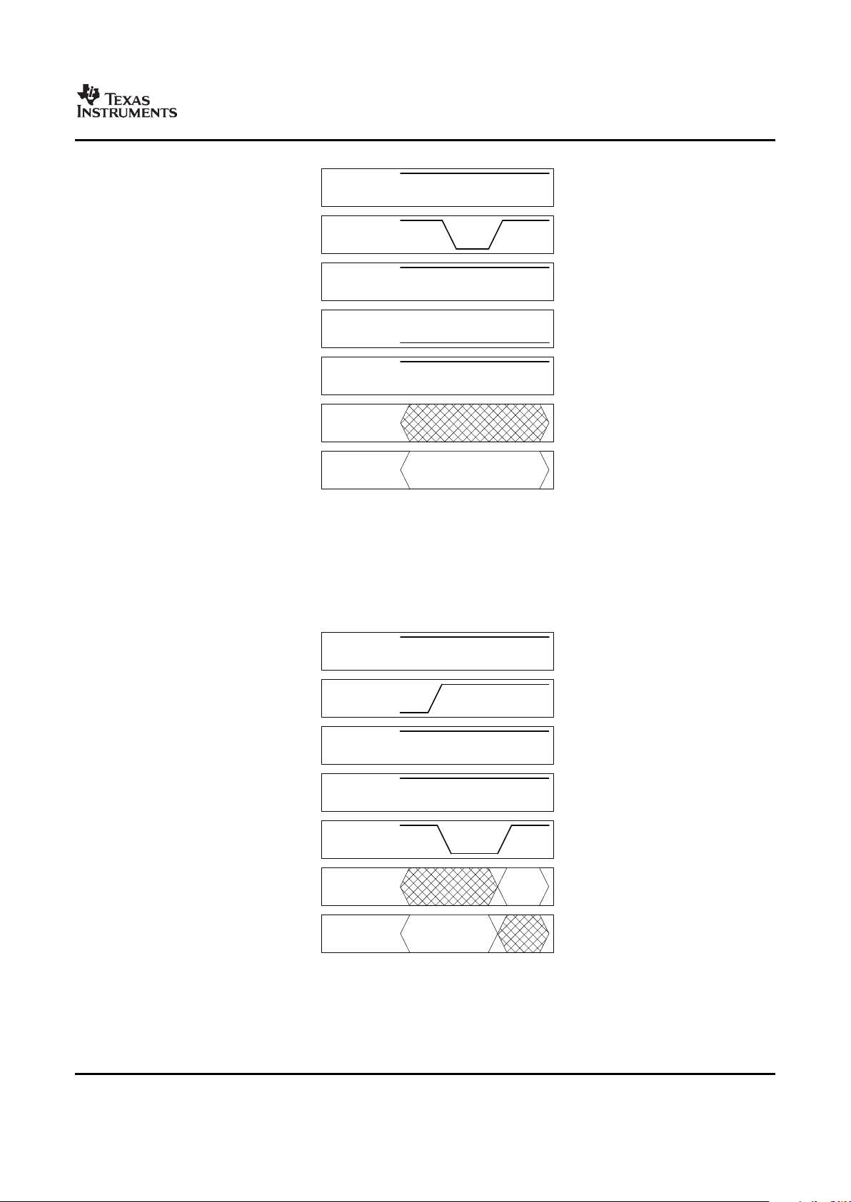
2. HPD Changes on the selected port. There are also two possible starting cases for this scenario:
– Case one: In this case only one HPD input is initially HIGH. The HPD output logic state follows the state
of the HPD input. If the HPD input pulses LOW, as may be the case if the Sink device is requesting an
interrupt, the HPD output to the source also pulses LOW for the same duration of time with a slight delay
Copyright © 2008, Texas Instruments Incorporated Submit Documentation Feedback 25
Product Folder Link(s): SN75DP122
www.ti.com
LP
Priority
HPD_A
0
1
0
1
0
1
HPD_B
0
1
HPD_OUT
0
1
Channel A
Z
0
1
ChannelB
0
1
HI-Z
DATA
LP
Priority
HPD_A
0
1
0
1
0
1
HPD_B
0
1
HPD_OUT
0
1
Channel A
Z
0
1
ChannelB
0
1
HI-Z
HI-Z
DATA
SN75DP122
SLLS892 – FEBRUARY 2008
(see Figure 39 ). The delay of this signal through the SN75DP128 is specified as t
PD(HPD)
. If the duration of
the LOW pulse is less then t
M(HPD)
, it may not be accurately repeated to the source. If the duration of the
LOW pulse exceeds t
T2(HPD)
, the device assumes that an unplug event has occurred and enters the low
power state (see Figure 40 ). Once the HPD input goes high again, the device returns to the active state
as indicated in scenario 1. The state of the Priority pin has no effect in this scenario as only one HPD
input port is active.
Figure 39.
Figure 40.
– Case two: In this case both HPD inputs are initially HIGH and the selected port has been determined by
the state of the priority pin. The HPD output logic state follows the state of the selected HPD input. If the
HPD input pulses LOW, the HPD output to the source also pulses LOW for the same duration of time,
again with a slight delay (see Figure 41 ). If the duration of the LOW pulse exceeds t
T2(HPD)
, the device
assumes that an unplug event has occurred and the other port is selected (see Figure 42 ). The case in
26 Submit Documentation Feedback Copyright © 2008, Texas Instruments Incorporated
Product Folder Link(s): SN75DP122
www.ti.com
LP
Priority
HPD_A
0
1
0
1
0
1
HPD_B
0
1
HPD_OUT
0
1
Channel A
Z
0
1
ChannelB
0
1
HI-Z
DATA
LP
Priority
HPD_A
0
1
0
1
0
1
HPD_B
0
1
HPD_OUT
0
1
Channel A
Z
0
1
ChannelB
0
1
HI-Z
DATA HI-Z
DATA
SN75DP122
SLLS892 – FEBRUARY 2008
which the previously selected port with priority goes high again is covered in scenario 3.
Figure 41.
Figure 42.
3. One channel becomes active while other channel is already selected. There are also two possible starting
cases for this scenario:
– Case one: In this case the HPD input that is initially HIGH is from the port that has priority. Since the port
with priority is already selected, any activity on the HPD input from the other port does not have any
effect on the switch whatsoever (see Figure 43 ).
Copyright © 2008, Texas Instruments Incorporated Submit Documentation Feedback 27
Product Folder Link(s): SN75DP122

www.ti.com
LP
Priority
HPD_A
0
1
0
1
0
1
HPD_B
0
1
HPD_OUT
0
1
Channel A
Z
0
1
ChannelB
0
1
HI-Z
DATA
LP
Priority
HPD_A
0
1
0
1
0
1
HPD_B
0
1
HPD_OUT
0
1
Channel A
Z
0
1
ChannelB
0
1
HI-Z
DATA HI-Z
DATA
SN75DP122
SLLS892 – FEBRUARY 2008
Figure 43.
– Case two: In this case the HPD input that is initially HIGH is not the port with priority. When the HPD input
of the port that has priority goes high, the HPD output is forced LOW for some time in order to simulate
an unplug event to the source device. The duration of this LOW output is defined as t
T2(HPD)
. If the HPD
input of the port with priority pulses LOW for a short duration while the t
T2(HPD)
timer is counting down, the
timer is reset. Once this time has passed the switch switches to the port with priority and the output HPD
once again follows the state of the newly selected channel ’ s HPD input (see Figure 44 ).
Figure 44.
4. 4. Priority pin is toggled. There are also two possible starting cases for this scenario:
– Case one: In this case only one HPD input is HIGH. A port whose HPD input is LOW cannot be selected.
In this case, the state of the priority pin has no effect on the switch (see Figure 45 ).
28 Submit Documentation Feedback Copyright © 2008, Texas Instruments Incorporated
Product Folder Link(s): SN75DP122
www.ti.com
LP
Priority
HPD_A
0
1
0
1
0
1
HPD_B
0
1
HPD_OUT
0
1
Channel A
Z
0
1
ChannelB
0
1
HI-Z
DATA
LP
Priority
HPD_A
0
1
0
1
0
1
HPD_B
0
1
HPD_OUT
0
1
Channel A
Z
0
1
ChannelB
0
1
HI-Z
DATA HI-Z
DATA
SN75DP122
SLLS892 – FEBRUARY 2008
Figure 45.
– Case two: In this case both HPD inputs are HIGH. Changing the state of the priority pin when both HPD
inputs are high forces the device to switch which channel is selected. When a state change is detected on
the priority pin, the device waits for a short period of time t
T1(HPD)
before responding (see Figure 46 ). The
purpose for this pause is to allow for the priority signal to settle and also to allow the device to ignore
potential glitches on the priority pin. Once t
T1(HPD)
has expired, the HPD output is forced LOW for t
T2(HPD)
and the device follows the chain of events outlined in scenario 3 case 2.
Figure 46.
Copyright © 2008, Texas Instruments Incorporated Submit Documentation Feedback 29
Product Folder Link(s): SN75DP122

PACKAGING INFORMATION
Orderable Device Status
(1)
Package
Type
Package
Drawing
Pins Package
Qty
Eco Plan
(2)
Lead/Ball Finish MSL Peak Temp
(3)
SN75DP122RTQR ACTIVE QFN RTQ 56 2000 Green (RoHS &
no Sb/Br)
CU NIPDAU Level-3-260C-168 HR
SN75DP122RTQRG4 ACTIVE QFN RTQ 56 2000 Green (RoHS &
no Sb/Br)
CU NIPDAU Level-3-260C-168 HR
SN75DP122RTQT ACTIVE QFN RTQ 56 250 Green (RoHS &
no Sb/Br)
CU NIPDAU Level-3-260C-168 HR
SN75DP122RTQTG4 ACTIVE QFN RTQ 56 250 Green (RoHS &
no Sb/Br)
CU NIPDAU Level-3-260C-168 HR
(1)
The marketing status values are defined as follows:
ACTIVE: Product device recommended for new designs.
LIFEBUY: TI has announced that the device will be discontinued, and a lifetime-buy period is in effect.
NRND: Not recommended for new designs. Device is in production to support existing customers, but TI does not recommend using this part in
a new design.
PREVIEW: Device has been announced but is not in production. Samples may or may not be available.
OBSOLETE: TI has discontinued the production of the device.
(2)
Eco Plan - The planned eco-friendly classification: Pb-Free (RoHS), Pb-Free (RoHS Exempt), or Green (RoHS & no Sb/Br) - please check
http://www.ti.com/productcontent for the latest availability information and additional product content details.
TBD: The Pb-Free/Green conversion plan has not been defined.
Pb-Free (RoHS): TI's terms "Lead-Free" or "Pb-Free" mean semiconductor products that are compatible with the current RoHS requirements
for all 6 substances, including the requirement that lead not exceed 0.1% by weight in homogeneous materials. Where designed to be soldered
at high temperatures, TI Pb-Free products are suitable for use in specified lead-free processes.
Pb-Free (RoHS Exempt): This component has a RoHS exemption for either 1) lead-based flip-chip solder bumps used between the die and
package, or 2) lead-based die adhesive used between the die and leadframe. The component is otherwise considered Pb-Free (RoHS
compatible) as defined above.
Green (RoHS & no Sb/Br): TI defines "Green" to mean Pb-Free (RoHS compatible), and free of Bromine (Br) and Antimony (Sb) based flame
retardants (Br or Sb do not exceed 0.1% by weight in homogeneous material)
(3)
MSL, Peak Temp. -- The Moisture Sensitivity Level rating according to the JEDEC industry standard classifications, and peak solder
temperature.
Important Information and Disclaimer:The information provided on this page represents TI's knowledge and belief as of the date that it is
provided. TI bases its knowledge and belief on information provided by third parties, and makes no representation or warranty as to the
accuracy of such information. Efforts are underway to better integrate information from third parties. TI has taken and continues to take
reasonable steps to provide representative and accurate information but may not have conducted destructive testing or chemical analysis on
incoming materials and chemicals. TI and TI suppliers consider certain information to be proprietary, and thus CAS numbers and other limited
information may not be available for release.
In no event shall TI's liability arising out of such information exceed the total purchase price of the TI part(s) at issue in this document sold by TI
to Customer on an annual basis.
PACKAGE OPTION ADDENDUM
www.ti.com
20-Mar-2008
Addendum-Page 1
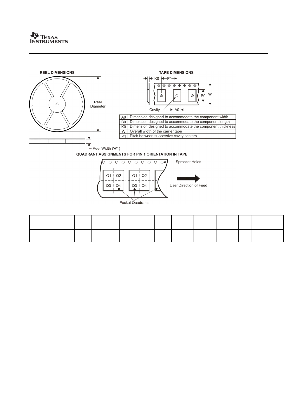
TAPE AND REEL INFORMATION
*All dimensions are nominal
Device Package
Type
Package
Drawing
Pins SPQ Reel
Diameter
(mm)
Reel
Width
W1 (mm)
A0 (mm) B0 (mm) K0 (mm) P1
(mm)W(mm)
Pin1
Quadrant
SN75DP122RTQR QFN RTQ 56 2000 330.0 16.4 8.3 8.3 2.25 12.0 16.0 Q2
SN75DP122RTQT QFN RTQ 56 250 180.0 16.4 8.3 8.3 2.25 12.0 16.0 Q2
PACKAGE MATERIALS INFORMATION
www.ti.com
11-Mar-2008
Pack Materials-Page 1

*All dimensions are nominal
Device Package Type Package Drawing Pins SPQ Length (mm) Width (mm) Height (mm)
SN75DP122RTQR QFN RTQ 56 2000 346.0 346.0 33.0
SN75DP122RTQT QFN RTQ 56 250 190.5 212.7 31.8
PACKAGE MATERIALS INFORMATION
www.ti.com
11-Mar-2008
Pack Materials-Page 2


IMPORTANT NOTICE
Texas Instruments Incorporated and its subsidiaries (TI) reserve the right to make corrections, modifications, enhancements, improvements,
and other changes to its products and services at any time and to discontinue any product or service without notice. Customers should
obtain the latest relevant information before placing orders and should verify that such information is current and complete. All products are
sold subject to TI’s terms and conditions of sale supplied at the time of order acknowledgment.
TI warrants performance of its hardware products to the specifications applicable at the time of sale in accordance with TI’s standard
warranty. Testing and other quality control techniques are used to the extent TI deems necessary to support this warranty. Except where
mandated by government requirements, testing of all parameters of each product is not necessarily performed.
TI assumes no liability for applications assistance or customer product design. Customers are responsible for their products and
applications using TI components. To minimize the risks associated with customer products and applications, customers should provide
adequate design and operating safeguards.
TI does not warrant or represent that any license, either express or implied, is granted under any TI patent right, copyright, mask work right,
or other TI intellectual property right relating to any combination, machine, or process in which TI products or services are used. Information
published by TI regarding third-party products or services does not constitute a license from TI to use such products or services or a
warranty or endorsement thereof. Use of such information may require a license from a third party under the patents or other intellectual
property of the third party, or a license from TI under the patents or other intellectual property of TI.
Reproduction of TI information in TI data books or data sheets is permissible only if reproduction is without alteration and is accompanied
by all associated warranties, conditions, limitations, and notices. Reproduction of this information with alteration is an unfair and deceptive
business practice. TI is not responsible or liable for such altered documentation. Information of third parties may be subject to additional
restrictions.
Resale of TI products or services with statements different from or beyond the parameters stated by TI for that product or service voids all
express and any implied warranties for the associated TI product or service and is an unfair and deceptive business practice. TI is not
responsible or liable for any such statements.
TI products are not authorized for use in safety-critical applications (such as life support) where a failure of the TI product would reasonably
be expected to cause severe personal injury or death, unless officers of the parties have executed an agreement specifically governing
such use. Buyers represent that they have all necessary expertise in the safety and regulatory ramifications of their applications, and
acknowledge and agree that they are solely responsible for all legal, regulatory and safety-related requirements concerning their products
and any use of TI products in such safety-critical applications, notwithstanding any applications-related information or support that may be
provided by TI. Further, Buyers must fully indemnify TI and its representatives against any damages arising out of the use of TI products in
such safety-critical applications.
TI products are neither designed nor intended for use in military/aerospace applications or environments unless the TI products are
specifically designated by TI as military-grade or "enhanced plastic." Only products designated by TI as military-grade meet military
specifications. Buyers acknowledge and agree that any such use of TI products which TI has not designated as military-grade is solely at
the Buyer's risk, and that they are solely responsible for compliance with all legal and regulatory requirements in connection with such use.
TI products are neither designed nor intended for use in automotive applications or environments unless the specific TI products are
designated by TI as compliant with ISO/TS 16949 requirements. Buyers acknowledge and agree that, if they use any non-designated
products in automotive applications, TI will not be responsible for any failure to meet such requirements.
Following are URLs where you can obtain information on other Texas Instruments products and application solutions:
Products Applications
Amplifiers amplifier.ti.com Audio www.ti.com/audio
Data Converters dataconverter.ti.com Automotive www.ti.com/automotive
DSP dsp.ti.com Broadband www.ti.com/broadband
Clocks and Timers www.ti.com/clocks Digital Control www.ti.com/digitalcontrol
Interface interface.ti.com Medical www.ti.com/medical
Logic logic.ti.com Military www.ti.com/military
Power Mgmt power.ti.com Optical Networking www.ti.com/opticalnetwork
Microcontrollers microcontroller.ti.com Security www.ti.com/security
RFID www.ti-rfid.com Telephony www.ti.com/telephony
RF/IF and ZigBee® Solutions www.ti.com/lprf Video & Imaging www.ti.com/video
Wireless www.ti.com/wireless
Mailing Address: Texas Instruments, Post Office Box 655303, Dallas, Texas 75265
Copyright © 2008, Texas Instruments Incorporated
 Loading...