

SN75C198
QUADRUPLE LOW-POWER LINE DRIVERS
SLLS051C – JULY 1990 – REVISED MARCH 1997
1
POST OFFICE BOX 655303 • DALLAS, TEXAS 75265
D
Meets ANSI EIA/TIA-232-E and ITU
Recommendation V.28
D
Very Low Supply Current
D
Sleep Mode:
3-State Outputs in High-Impedance State
Ultra-Low Supply Current...17 µA Typ
D
Improved Functional Replacement for:
SN75188,
Motorola MC1488,
National Semiconductor DS14C88, and
DS1488
D
CMOS- and TTL-Compatible Data Inputs
D
On-Chip Slew-Rate Limit...30 V/µs
D
Output Current Limit...10 mA Typ
D
Wide Supply Voltage Range...±4.5 V
to ±15 V
description
The SN75C198 is a monolithic low-power BI-MOS device containing four low-power line drivers designed to
interface data terminal equipment (DTE) with data circuit-terminating equipment (DCE) in conformance with the
specifications of ANSI EIA /TIA-232-E. The drivers of the SN75C198 are similar to those of the SN75C188
quadruple driver. The drivers have a controlled-output slew rate that is limited to a maximum of 30 V/µ s. This
feature eliminates the need for external components.
The sleep-mode input, SM
, can switch the outputs to high impedance, which avoids the transmission of
corrupted data during power-up and allows significant system power savings during data-off periods.
The SN75C198 is characterized for operation from 0°C to 70°C.
FUNCTION TABLE
INPUTS
OUTPUT
SM A B
Y
H H H L
H LX H
HXL H
LXX Z
H = high level, L = low level,
X = irrelevant, Z= high impedance
Copyright 1997, Texas Instruments Incorporated
PRODUCTION DATA information is current as of publication date.
Products conform to specifications per the terms of Texas Instruments
standard warranty. Production processing does not necessarily include
testing of all parameters.
Please be aware that an important notice concerning availability, standard warranty, and use in critical applications of
Texas Instruments semiconductor products and disclaimers thereto appears at the end of this data sheet.
1
2
3
4
5
6
7
14
13
12
11
10
9
8
V
CC–
1A
1Y
2A
2B
2Y
GND
V
CC+
SM
4A
4Y
3B
3A
3Y
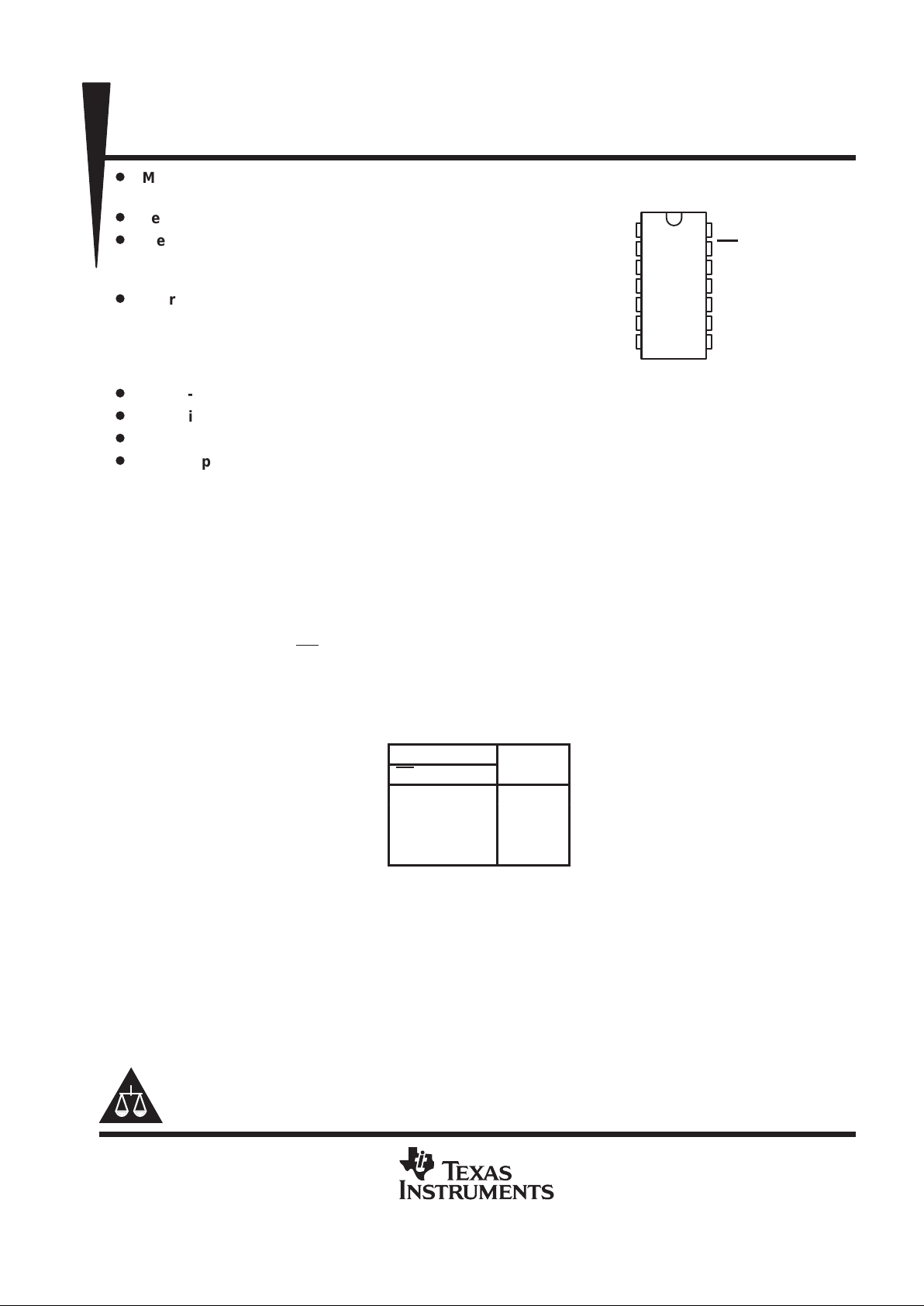
D OR N PACKAGE
(TOP VIEW)
NOT RECOMMENDED FOR NEW DESIGNS
SN75C198
QUADRUPLE LOW-POWER LINE DRIVERS
SLLS051C – JULY 1990 – REVISED MARCH 1997
2
POST OFFICE BOX 655303 • DALLAS, TEXAS 75265
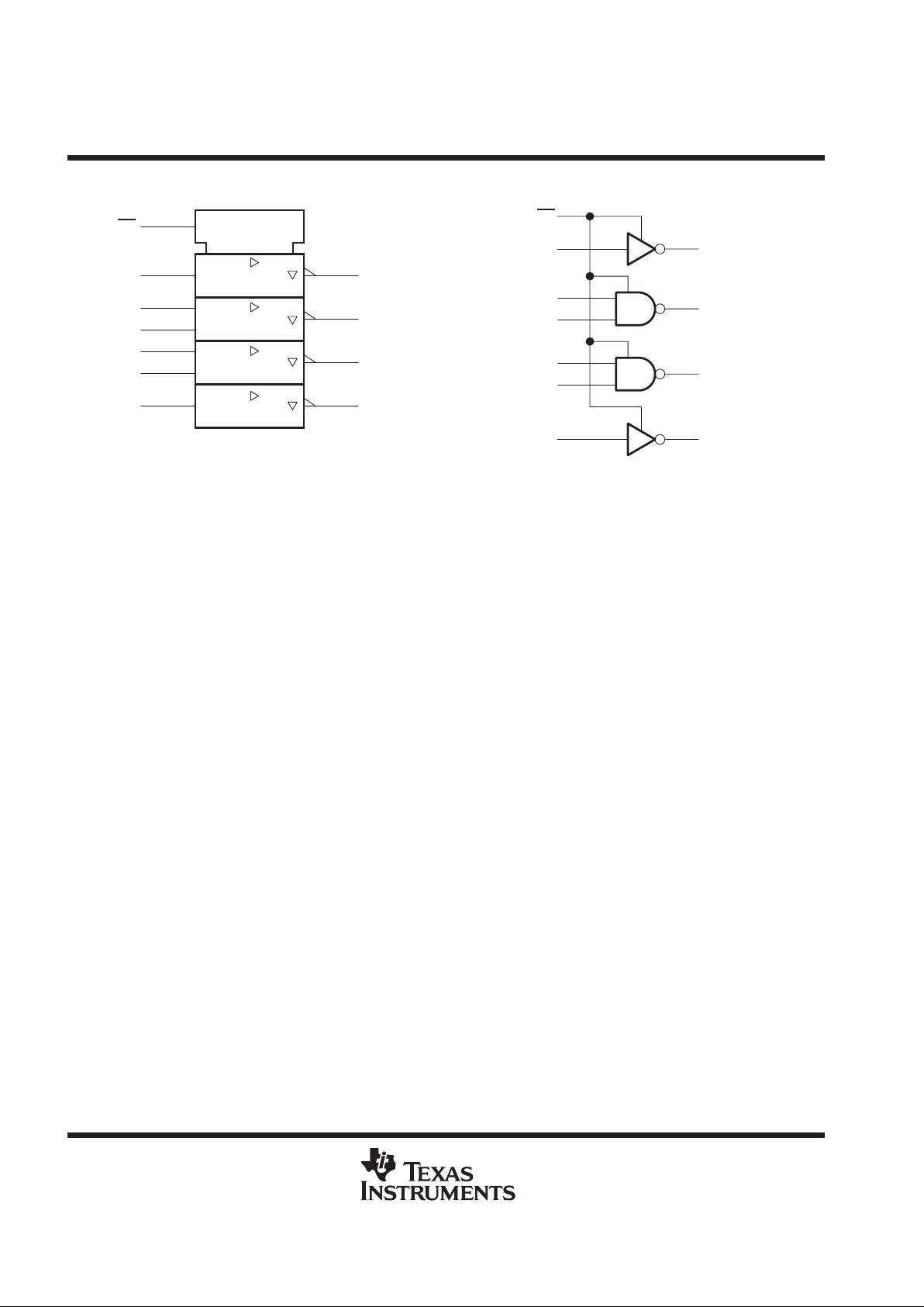
logic symbol
†
EN
&
&
4Y
3Y
2Y
1Y
12
10
9
5
4
2
13
4A
3B
3A
2B
2A
1A
SM
11
8
6
3
†
This symbol is in accordance with ANSI/IEEE Std 91-1984
and IEC Publication 617-12.
logic diagram (positive logic)
4Y
3Y
2Y
1Y
12
10
9
5
4
2
13
4A
3B
3A
2B
2A
1A
SM
11
8
6
3
SN75C198
QUADRUPLE LOW-POWER LINE DRIVERS
SLLS051C – JULY 1990 – REVISED MARCH 1997
3
POST OFFICE BOX 655303 • DALLAS, TEXAS 75265
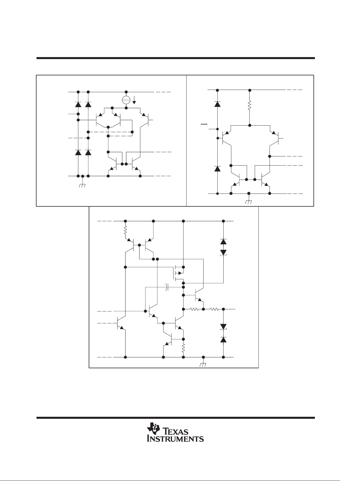
schematics of inputs and outputs
Input
V
CC +
SM
VCC±
EQUIVALENT OF SLEEP-MODE INPUT
V
CC –
and 3 Only)
(Drivers 2
Input B
Input A
V
CC+
to GND
Reference
1.4-V
Internal
and 4)
(Drivers 1
72 Ω
74 Ω
160 Ω
V
CC–
Output
V
CC+
EQUIVALENT OF A AND B INPUTS
TYPICAL OF Y OUTPUTS
to GND
Reference
1.4-V
Internal
All resistor values shown are nominal.
SN75C198
QUADRUPLE LOW-POWER LINE DRIVERS
SLLS051C – JULY 1990 – REVISED MARCH 1997
4
POST OFFICE BOX 655303 • DALLAS, TEXAS 75265
absolute maximum ratings over operating free-air temperature range (unless otherwise noted)
†
Supply voltage, V
CC+
(see Note 1) 15 V. . . . . . . . . . . . . . . . . . . . . . . . . . . . . . . . . . . . . . . . . . . . . . . . . . . . . . . . . . .
Supply voltage, V
CC–
–15 V. . . . . . . . . . . . . . . . . . . . . . . . . . . . . . . . . . . . . . . . . . . . . . . . . . . . . . . . . . . . . . . . . . . . .
Input voltage range, V
I
–15 V to 15 V. . . . . . . . . . . . . . . . . . . . . . . . . . . . . . . . . . . . . . . . . . . . . . . . . . . . . . . . . . . . . .
Output voltage range, V
O
V
CC–
–6 V to V
CC+
+ 6 V. . . . . . . . . . . . . . . . . . . . . . . . . . . . . . . . . . . . . . . . . . . . . . . .
Continuous total power dissipation See Dissipation Rating Table. . . . . . . . . . . . . . . . . . . . . . . . . . . . . . . . . . . . .
Operating free-air temperature range, T
A
: SN75C198 0°C to 70°C. . . . . . . . . . . . . . . . . . . . . . . . . . . . . . . . . .
Storage temperature range, T
stg
–65°C to 150°C. . . . . . . . . . . . . . . . . . . . . . . . . . . . . . . . . . . . . . . . . . . . . . . . . . .
Lead temperature 1,6 mm (1/16 inch) from case for 10 seconds 260°C. . . . . . . . . . . . . . . . . . . . . . . . . . . . . . .
†
Stresses beyond those listed under “absolute maximum ratings” may cause permanent damage to the device. These are stress ratings only, and
functional operation of the device at these or any other conditions beyond those indicated under “recommended operating conditions” is not
implied. Exposure to absolute-maximum-rated conditions for extended periods may affect device reliability.
NOTE 1: All voltages are with respect to the network ground terminal.
DISSIPATION RATING TABLE
T
≤ 25°C DERATING FACTOR T
= 70°C
PACKAGE
A
POWER RATING ABOVE TA = 25°CAPOWER RATING
D 950 mW 7.6 mW/°C 608 mW
N 1150 mW 9.2 mW/°C 730 mW
recommended operating conditions
MIN NOM MAX UNIT
Supply voltage, V
CC+
4.5 12 15 V
Supply voltage, V
CC–
–4.5 –12 –15 V
Input voltage, VI (see Figure 2) V
CC–
+2 V
CC+
V
High-level input voltage, V
IH
2 V
p
A and B inputs 0.8
Low-level input voltage, V
IL
SM input 0.6
V
Operating free-air temperature, T
A
0 70 ° C

SN75C198
QUADRUPLE LOW-POWER LINE DRIVERS
SLLS051C – JULY 1990 – REVISED MARCH 1997
5
POST OFFICE BOX 655303 • DALLAS, TEXAS 75265
electrical characteristics over recommended operating free-air temperature range, V
CC
±
= ±12 V,
SM
at 2 V (unless otherwise noted)
PARAMETER TEST CONDITIONS MIN TYP†MAX UNIT
p
V
CC±
= ±5 V 4
VOHHigh-level output voltage
V
IH
= 0.8 V,
R
L
= 3
kΩ
V
CC±
= ±12 V 10
V
p
V
CC±
= ±5 V –4
VOLLow-level output voltage (see Note 2)
V
IH
= 2 V,
R
L
= 3
kΩ
V
CC±
= ±12 V –10
V
I
IH
High-level input current VI = 5 V 10 µA
I
IL
Low-level input current VI = 0 V –10 µA
V
= 12 V,
p
p
O
,
V
CC±
= ±12 V
100
IOZHigh-impedance-state output current
SM at 0.6 V
V
= –12 V ,
µ
A
O
,
V
CC±
= ±12 V
–
100
I
OS(H)
High-level short-circuit output current‡VI = 0.8 V, VO = 0 or V
CC–
–4.5 –10 –19.5 mA
I
OS(L)
Low-level short-circuit output current‡VI = 2 V, VO = 0 or V
CC+
4.5 10 19.5 mA
r
o
Output resistance V
CC±
= 0, VO = –2 V to 2 V 300 Ω
A and B inputs at 0.8 V or 2 V,
V
CC±
= ±5 V 90 160
pp
,
No load
V
CC±
= ±12 V 95 160
I
CC+
Supply current from V
CC+
A and B inputs at 0.8 V or 2 V,
V
CC±
= ±5 V 40
µ
A
,
RL = 3 kΩ,SM at 0.6 V
V
CC±
= ±12 V 40
A and B inputs at 0.8 V or 2 V,
V
CC±
= ±5 V –90 –160
pp
,
No load
V
CC±
= ±12 V –95 –160
I
CC–
Supply current from V
CC–
A and B inputs at 0.8 V or 2 V,
V
CC±
= ±5 V –40
µ
A
RL = 3 kΩ,SM at 0.6 V
V
CC±
= ±12 V –40
†
All typical values are at TA = 25°C.
‡
Not more than one output should be shorted at a time.
NOTE 2: The algebraic convention, where the more positive (less negative) limit is designated as maximum, is used in this data sheet for logic
levels only, e.g., if –10 V is a maximum, the typical value is a more negative voltage.
switching characteristics over recommended operating free-air temperature range, V
CC
±
= ±12 V
(unless otherwise noted)
PARAMETER TEST CONDITIONS MIN TYP†MAX UNIT
t
PLH
Propagation delay time, low- to high-level output
§
3 µs
t
PHL
Propagation delay time, high- to low-level output
§
R
= 3 kΩ to 7 kΩ, C
= 15 pF,
3.5 µs
t
TLH
Transition time, low- to high-level output
¶
L
,
See Figure 1
L
,
0.53 1 3.2 µs
t
THL
Transition time, high- to low-level output
¶
0.53 1 3.2 µs
t
TLH
Transition time, low- to high-level output
#
R
= 3 kΩ to 7 kΩ, C
= 2500 pF,
1.5 µs
t
THL
Transition time, high- to low-level output
#
L
,
See Figure 2
L
,
1.5 µs
t
PZH
Output enable time to high level
R
= 3 kΩ to 7 kΩ, C
= 15 pF,
50 µs
t
PHZ
Output disable time from high level
L
,
See Figure 3
L
,
10 µs
t
PZL
Output enable time to low level
R
= 3 kΩ to 7 kΩ, C
= 15 pF,
15 µs
t
PLZ
Output disable time from low level
L
,
See Figure 4
L
,
10 µs
SR Output slew rate
#
RL = 3 kΩ to 7 kΩ, CL = 15 pF 6 15 30 V/µs
†
All typical values are at TA = 25°C.
§
t
PHL
and t
PLH
include the additional time due to on-chip slew rate and are measured at the 50% points.
¶
Measured between 10% and 90% points of output waveform
#
Measured between 3-V and –3-V points of output waveform

SN75C198
QUADRUPLE LOW-POWER LINE DRIVERS
SLLS051C – JULY 1990 – REVISED MARCH 1997
6
POST OFFICE BOX 655303 • DALLAS, TEXAS 75265
PARAMETER MEASUREMENT INFORMATION
TEST CIRCUIT VOLTAGE WAVEFORMS
Output
Input
10%
50%
90%
t
PHL
t
PLH
V
OL
V
OH
0 V
3 V
(see Note B)
C
L
R
L
Output
Input
t
THL
t
TLH
Pulse
Generator
(see Note A)
NOTES: A. The pulse generator has the following characteristics: tw = 25 µs, PRR = 20 kHz, ZO = 50 Ω, tr = tf ≤50 ns.
B. CL includes probe and jig capacitance.
Figure 1. Test Circuit and Voltage Waveforms, Propagation and Transition Times
Input
Pulse
TEST CIRCUIT
Output
C
L
(see Note B)
Generator
(see Note A)
R
L
3 V
0 V
V
OH
V
OL
3 V
–3 V–3 V
3 V
t
THL
t
TLH
VOLTAGE WAVEFORMS
Output
Input
NOTES: A. The pulse generator has the following characteristics: tw = 25 µs, PRR = 20 kHz, ZO = 50 Ω, tr = tf ≤50 ns.
B. CL includes probe and jig capacitance.
Figure 2. Test Circuit and Voltage Waveforms, Transition Times
Input
TEST CIRCUIT
Output
C
L
(see Note B)
R
L
3 V
0 V
V
OH
V
off
≈ 0 V
t
PHZ
VOLTAGE WAVEFORMS
V
OH/2
t
PZH
1.5 V 1.5 V
0.5 V
0 V
Pulse
Generator
(see Note A)
Input
Output
NOTES: A. The pulse generator has the following characteristics: tw = 25 µs, PRR = 20 kHz, ZO = 50 Ω, tr = tf ≤50 ns.
B. CL includes probe and jig capacitance.
Figure 3. Driver Test Circuit and Voltage Waveforms

SN75C198
QUADRUPLE LOW-POWER LINE DRIVERS
SLLS051C – JULY 1990 – REVISED MARCH 1997
7
POST OFFICE BOX 655303 • DALLAS, TEXAS 75265
PARAMETER MEASUREMENT INFORMATION
Input
TEST CIRCUIT
Output
C
L
(see Note B)
R
L
3 V
0 V
V
OL
V
off
≈ 0 V
t
PZL
VOLTAGE WAVEFORMS
V
OL/2
1.5 V 1.5 V
t
PLZ
3 V
0.5 V
Pulse
Generator
(see Note A)
Input
Output
NOTES: A. The pulse generator has the following characteristics: tw = 25 µs, PRR = 20 kHz, ZO = 50 Ω, tr = tf ≤50 ns.
B. CL includes probe and jig capacitance.
Figure 4. Driver Test Circuit and Voltage Waveforms

SN75C198
QUADRUPLE LOW-POWER LINE DRIVERS
SLLS051C – JULY 1990 – REVISED MARCH 1997
8
POST OFFICE BOX 655303 • DALLAS, TEXAS 75265
TYPICAL CHARACTERISTICS
V
CC±
= ±9 V
0
VI – Input Voltage – V
–15
20.2 0.4 0.6 0.8 1 1.2 1.4 1.6 1.8
–9
–6
–3
0
3
6
9
–12
RL = 3 kΩ
TA = 25°C
VO – Output Voltage – V
VOLTAGE TRANSFER CHARACTERISTICS
V
CC±
= ±5 V
V
CC±
= ±9 V
V
CC±
= ±12 V
V
CC±
= ±15 V
V
CC±
= ±15 V
V
CC±
= ±12 V
V
O
V
CC±
= ±5 V
Figure 5 Figure 6
–16
VO – Output Voltage – V
20
16
–20
–12 –8 –4 0 4 8 12
–16
–12
–8
–4
0
4
8
12
16
V
CC±
= ±12 V
TA = 25°C
VOH (VI = 0.8 V)
IO – Output Current – mA
OUTPUT CURRENT
vs
OUTPUT VOLTAGE
3-kΩ Load Line
VOL (VI = 2 V)
I
O
15
–15
–10
0
5
10
100806040200 120
TA – Free-Air Temperature – °C
VO = 0 or V
CC–
IOS – Short-Circuit Output Current – mA
SHORT-CIRCUIT OUTPUT CURRENT
vs
FREE-AIR TEMPERATURE
–5
OS
I
V
CC±
= ±12 V
I
OS(L)
VI = 2 V
VO = 0 or V
CC+
I
OS(H)
VI = 0.8 V
Figure 7 Figure 8
TA – Free-Air Temperature – °C
12
120
–12
0 20 40 60 80 100
–8
–4
0
4
8
VO – Output Voltage – V
OUTPUT VOLTAGE
vs
FREE-AIR TEMPERATURE
V
O
RL = 3 kΩ
VOH (V
CC±
= ± 12 V, VI = 0.8 V)
VOH (V
CC±
= ± 5 V, VI = 0.8 V)
VOL (V
CC±
= ± 5 V, VI = 2 V)
VOL (V
CC±
= ± 12 V, VI = 2 V)

SN75C198
QUADRUPLE LOW-POWER LINE DRIVERS
SLLS051C – JULY 1990 – REVISED MARCH 1997
9
POST OFFICE BOX 655303 • DALLAS, TEXAS 75265
TYPICAL CHARACTERISTICS
Figure 9
TA – Free-Air Temperature – °C
120
120
–40
0 20 40 60 80 100
–20
0
20
40
60
80
100
V
CC±
= ±12 V
IIH (VI = 5 V)
IIL (VI = 0)
II – Input Current – nA
INPUT CURRENT
vs
FREE-AIR TEMPERATURE
I
I
– Power-Off Output Resistance –
500
300
350
400
450
100806040200 120
TA – Free-Air Temperature – °C
V
CC±
= 0
VO = 2 V
POWER-OFF OUTPUT RESISTANCE
vs
FREE-AIR TEMPERATURE
Ωr
o
VO = – 2 V
325
375
425
475
Figure 10
RL = No Load
VI = 0.8 V or 2 V
– Supply Current –
120
–120
–80
–40
0
40
80
I
CC+
100806040200 120
TA – Free-Air Temperature – °C
SUPPLY CURRENT
vs
FREE-AIR TEMPERATURE
Aµ
V
CC±
= ±12 V
V
CC±
= ±5 V
V
CC±
= ±12 V
V
CC±
= ±5 V
I
CC–
CC ±
I
Figure 11 Figure 12
30
0
10
20
100806040200 120
TA – Free-Air Temperature – °C
RL = 3 kΩ
RL = 7 kΩ
RL = 3 kΩ
SR – Output Slew Rate – V/s
OUTPUT SLEW RATE
vs
FREE-AIR TEMPERATURE
µsV/
Slew Rate
Positive Transition
5
15
25
Slew Rate
Negative
Transition
RL =73 kΩ

SN75C198
QUADRUPLE LOW-POWER LINE DRIVERS
SLLS051C – JULY 1990 – REVISED MARCH 1997
10
POST OFFICE BOX 655303 • DALLAS, TEXAS 75265
TYPICAL CHARACTERISTICS
Figure 13
tpd – Propagation Delay Time – s
TA – Free-Air Temperature – °C
2
120
0
0 20406080100
0.5
1
1.5
t
PHL
t
PLH
RL = 3 kΩ
RL = 7 kΩ
RL = 7 kΩ
RL = 3 kΩ
PROPAGATION DELAY TIME
vs
FREE-AIR TEMPERATURE
t
pd
sµ
1.75
1.25
0.75
0.25
V
CC±
= ±12 V
CL = 15 pF
1.5
0.5
0
2
100806040200 120
TA – Free-Air Temperature – °C
t
THL
t
TLH
t
THL
t
TLH
CL = 2500 pF
CL = 15 pF
1
– Output Transition T ime –
OUTPUT TRANSITION TIME
vs
FREE-AIR TEMPERATURE
t
t
sµ
1.75
1.25
0.75
0.25
VCC± = ±12 V
RL = 3 kΩ to 7 kΩ
Figure 14
Figure 15
OUTPUT ENABLE TIME TO HIGH LEVEL
vs
FREE-AIR TEMPERATURE
30
120
0
0
20 40 60 80 100
5
10
15
20
25
TA – Free-Air Temperature – °C
tPZH – Output Enable Time to High Level – us
PZH
t
sµ
VCC± = ±12 V
RL = 3 kΩ
CL = 15 pF
Figure 16
0.7
0.6
0.5
0.4
0.3
100806040200
0.2
120
0.8
OUTPUT DISABLE TIME FROM HIGH LEVEL
vs
FREE-AIR TEMPERATURE
TA – Free-Air Temperature – °C
tPHZ – Output Disable Time From High Level –
PHZ
t
sµ
VCC± = ±12 V
RL = 3 kΩ
CL = 15 pF

SN75C198
QUADRUPLE LOW-POWER LINE DRIVERS
SLLS051C – JULY 1990 – REVISED MARCH 1997
11
POST OFFICE BOX 655303 • DALLAS, TEXAS 75265
TYPICAL CHARACTERISTICS
VCC± = ±12 V
RL = 3 kΩ
CL = 15 pF
tPZL – Output Enable Time to Low Level – us
OUTPUT ENABLE TIME TO LOW LEVEL
vs
FREE-AIR TEMPERATURE
7
6
5
4
3
2
1
100806040200
0
120
8
TA – Free-Air Temperature – °C
PZL
t
sµ
Figure 17 Figure 18
OUTPUT DISABLE TIME FROM LOW LEVEL
vs
FREE-AIR TEMPERATURE
3
0
0.5
1
1.5
2
2.5
100806040200 120
TA – Free-Air Temperature – °C
tPZL – Output Disable Time From Low Level – us
PLZ
t
sµ
VCC± = ±12 V
RL = 3 kΩ
CL = 15 pF

IMPORTANT NOTICE
T exas Instruments and its subsidiaries (TI) reserve the right to make changes to their products or to discontinue
any product or service without notice, and advise customers to obtain the latest version of relevant information
to verify, before placing orders, that information being relied on is current and complete. All products are sold
subject to the terms and conditions of sale supplied at the time of order acknowledgement, including those
pertaining to warranty, patent infringement, and limitation of liability.
TI warrants performance of its semiconductor products to the specifications applicable at the time of sale in
accordance with TI’s standard warranty. Testing and other quality control techniques are utilized to the extent
TI deems necessary to support this warranty. Specific testing of all parameters of each device is not necessarily
performed, except those mandated by government requirements.
CERT AIN APPLICATIONS USING SEMICONDUCTOR PRODUCTS MAY INVOLVE POTENTIAL RISKS OF
DEATH, PERSONAL INJURY, OR SEVERE PROPERTY OR ENVIRONMENTAL DAMAGE (“CRITICAL
APPLICATIONS”). TI SEMICONDUCTOR PRODUCTS ARE NOT DESIGNED, AUTHORIZED, OR
WARRANTED TO BE SUITABLE FOR USE IN LIFE-SUPPORT DEVICES OR SYSTEMS OR OTHER
CRITICAL APPLICATIONS. INCLUSION OF TI PRODUCTS IN SUCH APPLICA TIONS IS UNDERST OOD TO
BE FULLY AT THE CUSTOMER’S RISK.
In order to minimize risks associated with the customer’s applications, adequate design and operating
safeguards must be provided by the customer to minimize inherent or procedural hazards.
TI assumes no liability for applications assistance or customer product design. TI does not warrant or represent
that any license, either express or implied, is granted under any patent right, copyright, mask work right, or other
intellectual property right of TI covering or relating to any combination, machine, or process in which such
semiconductor products or services might be or are used. TI’s publication of information regarding any third
party’s products or services does not constitute TI’s approval, warranty or endorsement thereof.
Copyright 1998, Texas Instruments Incorporated
 Loading...