

SN75C189, SN75C189A
QUADRUPLE LOW-POWER LINE RECEIVERS
SLLS041G – OCTOBER 1988 – REVISED JANUARY 2000
1
POST OFFICE BOX 655303 • DALLAS, TEXAS 75265
D
Meet or Exceed the Requirements of
TIA/EIA-232-F and ITU Recommendation
V.28
D
Low Supply Current ...420 µA Typ
D
Preset On-Chip Input Noise Filter
D
Built-in Input Hysteresis
D
Response and Threshold Control Inputs
D
Push-Pull Outputs
D
Functionally Interchangeable and
Pin-to-Pin Compatible With
T exas Instruments SN75189/SN75189A and
Motorola MC1489/MC1489A
D
Package Options Include Plastic
Small-Outline (D) and Shrink Small-Outline
(DB) Packages, and Standard Plastic (N)
DIP
description
The SN75C189 and SN75C189A are low-power , bipolar, quadruple line receivers that are used to interface data
terminal equipment (DTE) with data circuit-terminating equipment (DCE). These devices have been designed
to conform to TIA/EIA-232-F.
The SN75C189 has a 0.33-V typical hysteresis, compared with 0.97 V for the SN75C189A. Each receiver has
provision for adjustment of the overall input threshold levels. This is achieved by choosing external series
resistors and voltages to provide bias levels for the response-control pins. The output is in the high logic state
if the input is open circuit or shorted to ground.
These devices have an on-chip filter that rejects input pulses of less than 1-µs duration. An external capacitor
can be connected from the control pins to ground to provide further input noise filtering for each receiver.
The SN75C189 and SN75C189A have been designed using low-power techniques in a bipolar technology . In
most applications, these receivers interface to single inputs of peripheral devices such as UARTs, ACEs, or
microprocessors. By using sampling, such peripheral devices usually are insensitive to the transition times of
the input signals. If this is not the case, or for other uses, it is recommended that the SN75C189 and SN75C189A
outputs be buffered by single Schmitt input gates or single gates of the HCMOS, ALS, or 74F logic families.
The SN75C189 and SN75C189A are characterized for operation from 0°C to 70°C.
Copyright 2000, Texas Instruments Incorporated
PRODUCTION DATA information is current as of publication date.
Products conform to specifications per the terms of Texas Instruments
standard warranty. Production processing does not necessarily include
testing of all parameters.
Please be aware that an important notice concerning availability, standard warranty, and use in critical applications of
Texas Instruments semiconductor products and disclaimers thereto appears at the end of this data sheet.
1
2
3
4
5
6
7
14
13
12
11
10
9
8
1A
1 CONT
1Y
2A
2 CONT
2Y
GND
V
CC
4A
4 CONT
4Y
3A
3 CONT
3Y
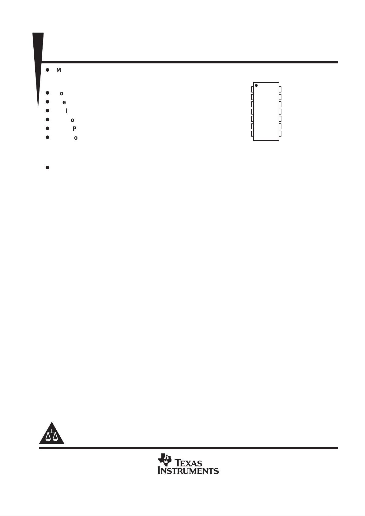
D, DB, OR N PACKAGE
(TOP VIEW)
SN75C189, SN75C189A
QUADRUPLE LOW-POWER LINE RECEIVERS
SLLS041G – OCTOBER 1988 – REVISED JANUARY 2000
2
POST OFFICE BOX 655303 • DALLAS, TEXAS 75265
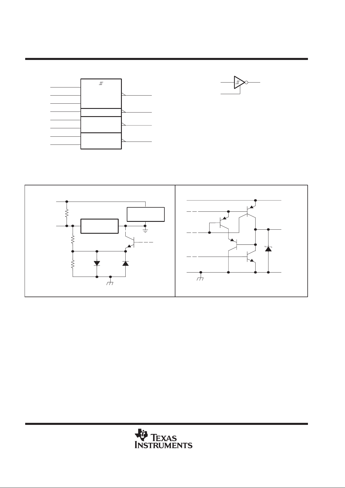
logic symbol
†
†
This symbol is in accordance with ANSI/IEEE Std 91-1984 and
IEC Publication 617-12.
1
1A
2
1 CONT
4
2A
5
2 CONT
10
3A
9
3 CONT
13
4A
12
4 CONT
1Y
3
2Y
6
3Y
8
4Y
11
THRESHOLD
ADJUST
logic diagram (each receiver)
Response
Control
A
Y
schematic of inputs and outputs
ESD
Protection
Input
3.4 kΩ
1.5 kΩ
530 Ω
V
CC
Output
EQUIVALENT OF EACH INPUT
‡
EQUIVALENT OF EACH OUTPUT
Response
Control
ESD
Protection
‡
All resistor values shown are nominal.
absolute maximum ratings over operating free-air temperature range (unless otherwise noted)
§
Supply voltage, VCC (see Note 1) 7 V. . . . . . . . . . . . . . . . . . . . . . . . . . . . . . . . . . . . . . . . . . . . . . . . . . . . . . . . . . . . .
Input voltage range, VI –30 V to 30 V. . . . . . . . . . . . . . . . . . . . . . . . . . . . . . . . . . . . . . . . . . . . . . . . . . . . . . . . . . . . . .
Output voltage range, V
O
–0.3 V to VCC+ 0.3 V. . . . . . . . . . . . . . . . . . . . . . . . . . . . . . . . . . . . . . . . . . . . . . . . . . . .
Package thermal impedance, θJA (see Note 2): D package 86°C/W. . . . . . . . . . . . . . . . . . . . . . . . . . . . . . . . . . .
DB package 96°C/W. . . . . . . . . . . . . . . . . . . . . . . . . . . . . . . . .
N package 80°C/W. . . . . . . . . . . . . . . . . . . . . . . . . . . . . . . . . . .
Lead temperature 1,6 mm (1/16 inch) from case for 10 seconds 260°C. . . . . . . . . . . . . . . . . . . . . . . . . . . . . . .
Storage temperature range, T
stg
–65°C to 150°C. . . . . . . . . . . . . . . . . . . . . . . . . . . . . . . . . . . . . . . . . . . . . . . . . . .
§
Stresses beyond those listed under “absolute maximum ratings” may cause permanent damage to the device. These are stress ratings only, and
functional operation of the device at these or any other conditions beyond those indicated under “recommended operating conditions” is not
implied. Exposure to absolute-maximum-rated conditions for extended periods may affect device reliability.
NOTES: 1. All voltages are with respect to network GND.
2. The package thermal impedance is calculated in accordance with JESD 51.
SN75C189, SN75C189A
QUADRUPLE LOW-POWER LINE RECEIVERS
SLLS041G – OCTOBER 1988 – REVISED JANUARY 2000
3
POST OFFICE BOX 655303 • DALLAS, TEXAS 75265
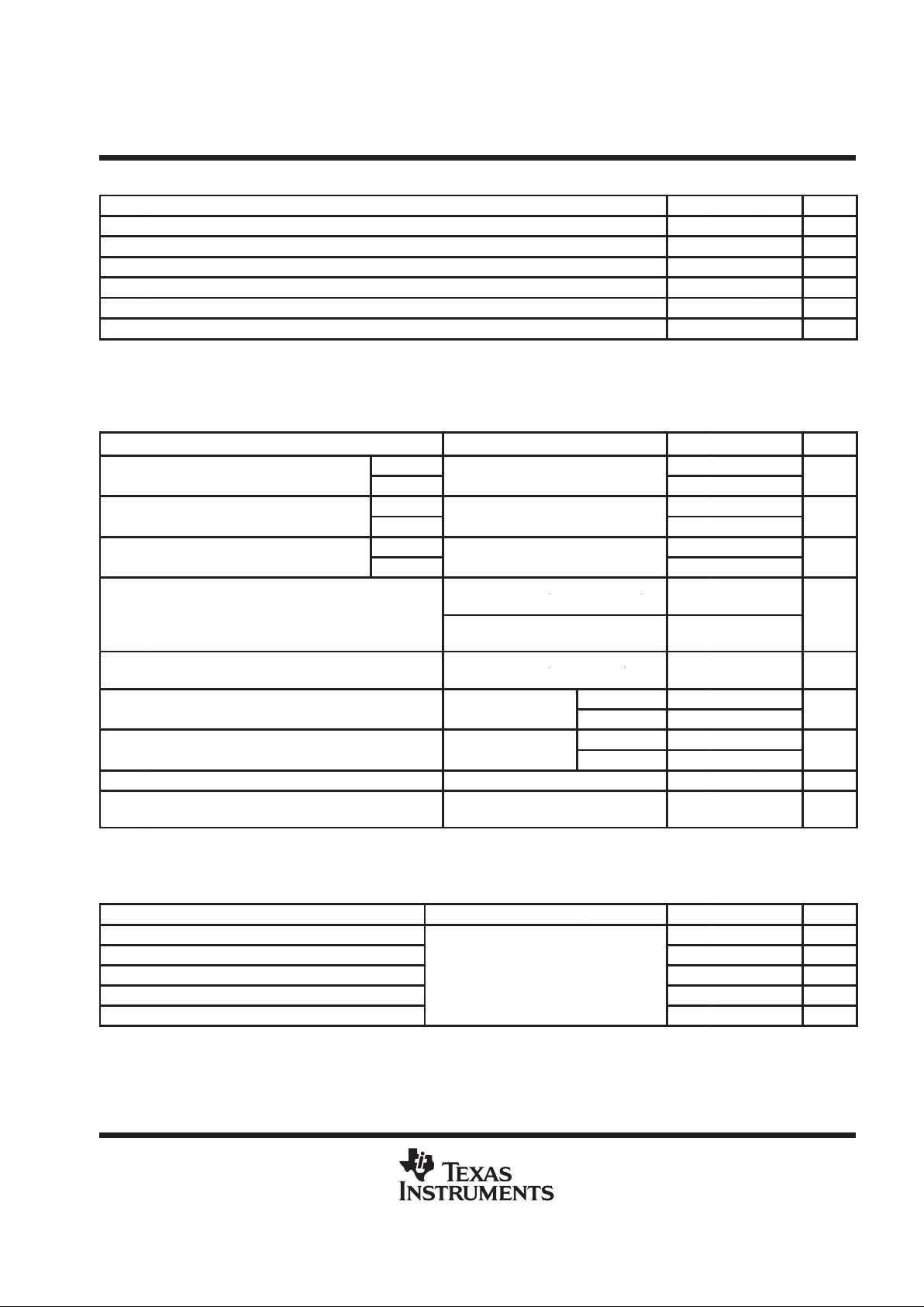
recommended operating conditions
MIN NOM MAX UNIT
V
CC
Supply voltage 4.5 5 6 V
V
I
Input voltage (see Note 3) –25 25 V
I
OH
High-level output current –3.2 mA
I
OL
Low-level output current 3.2 mA
Response-control current ±1 mA
T
A
Operating free-air temperature 0 70 °C
NOTE 3: The algebraic convention, where the more positive (less negative) limit is designated as maximum, is used in this data sheet for logic
levels only, e.g., if –10 V is a maximum, the typical value is a more negative voltage.
electrical characteristics over recommended free-air temperature range, VCC = 5 V ±10% (unless
otherwise noted) (see Note 4)
PARAMETER TEST CONDITIONS MIN
TYP
†
MAX UNIT
p
’C189
1 1.5
V
IT+
Positive-going input threshold voltage
’C189A
See Figure 1
1.6 2.25
V
p
’C189
0.75 1.25
V
IT–
Negative-going input threshold voltage
’C189A
See Figure 1
0.75 1 1.25
V
p
’C189
0.15 0.33
V
hys
Input hysteresis voltage (V
IT+
–
V
IT–
)
’C189A
See Figure 1
0.65 0.97
V
V
= 4.5 V to 6 V, V
= 0.75 V ,
p
CC
,
IOH = –20 µA
I
,
3.5
VOHHigh-level output voltage
VCC = 4.5 V to 6 V,
IOH = –3.2 mA
VI = 0.75 V ,
2.5
V
p
V
= 4.5 V to 6 V, V
= 3 V,
VOLLow-level output voltage
CC
,
IOL = 3.2 mA
I
,
0.4 V
p
VI = 25 V 3.6 8.3
IIHHigh-level input current
See Figure 2
VI = 3 V 0.43 1
mA
p
VI = –25 V –3.6 –8.3
IILLow-level input current
See Figure 2
VI = –3 V –0.43 –1
mA
I
OS
Short-circuit output current See Figure 3 –35 mA
I
CC
Supply current
VI = 5 V,
See Figure 2
No load,
420 700 µA
†
All typical values are at TA = 25°C.
NOTE 4: All characteristics are measured with response-control terminal open.
switching characteristics, VCC = 5 V ±10%, TA = 25°C
PARAMETER TEST CONDITIONS MIN TYP MAX UNIT
t
PLH
Propagation delay time, low- to high-level output 6 µs
t
PHL
Propagation delay time, high- to low-level output 6 µs
t
TLH
Transition time, low- to high-level output
‡
RL = 5 kΩ, CL = 50 pF, See Figure 4
500 ns
t
THL
Transition time, high- to low-level output
‡
300 ns
t
w(N)
Duration of longest pulse rejected as noise
§
1 6 µs
‡
Measured between 10% and 90% points of output waveform
§
The receiver ignores any positive- or negative-going pulse that is less than the minimum value of t
w(N)
and accepts any postive- or negative-going
pulse greater than the maximum of t
w(N)
.
SN75C189, SN75C189A
QUADRUPLE LOW-POWER LINE RECEIVERS
SLLS041G – OCTOBER 1988 – REVISED JANUARY 2000
4
POST OFFICE BOX 655303 • DALLAS, TEXAS 75265
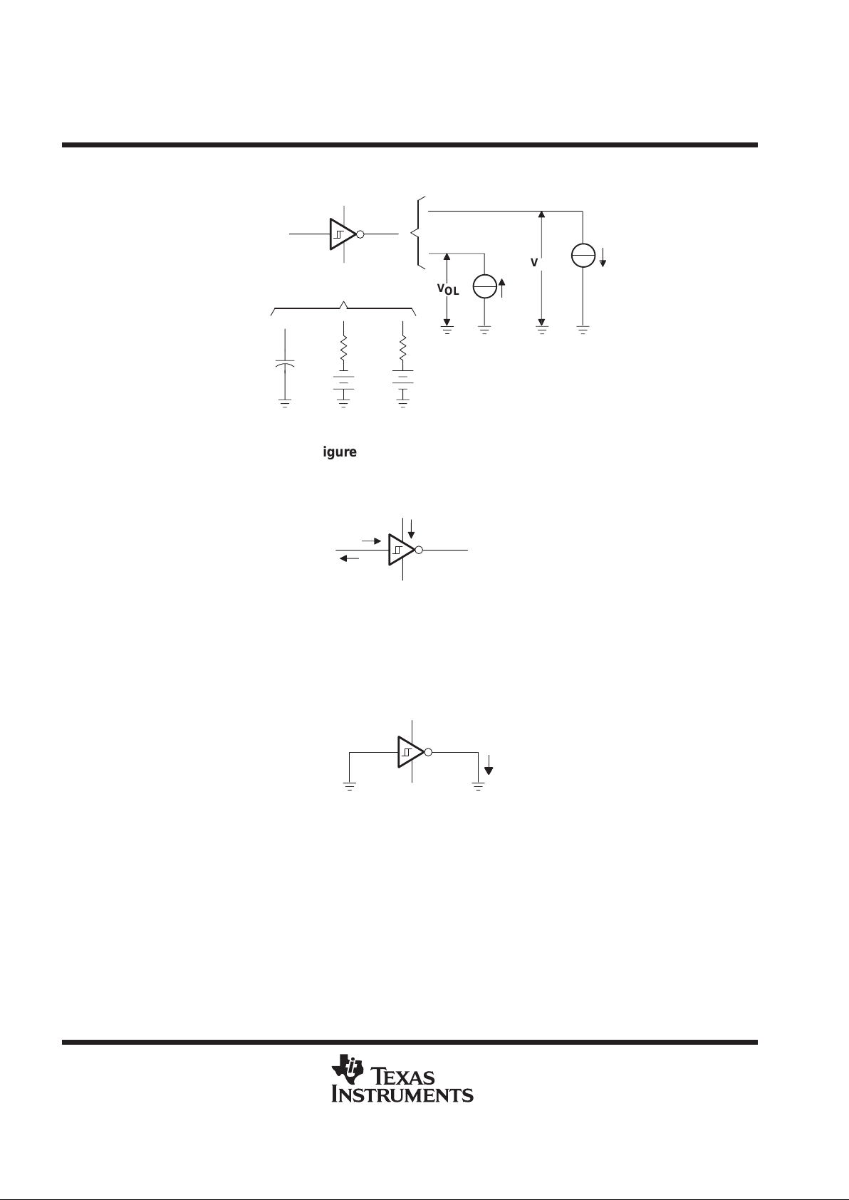
PARAMETER MEASUREMENT INFORMATION
Open Unless
Otherwise Specified
C
C
–V
C
R
C
V
C
R
C
Response
Control
VIT, V
1
V
CC
I
OL
–I
OH
NOTE A: Arrows indicate actual direction of current flow. Current into a terminal is a positive value.
V
OL
V
OH
Figure 1. VT+, V
IT–
, VOH, V
OL
–I
IL
V
I
I
IH
V
CC
I
CC
Open
NOTE A: Arrows indicate actual direction of current flow. Current into a terminal is a positive value.
Response Control
Open
Figure 2. IIH, IIL, I
CC
–I
OS
NOTE A: Arrows indicate actual direction of current flow. Current into a terminal is a positive value.
V
CC
Response Control
Open
Figure 3. I
OS

SN75C189, SN75C189A
QUADRUPLE LOW-POWER LINE RECEIVERS
SLLS041G – OCTOBER 1988 – REVISED JANUARY 2000
5
POST OFFICE BOX 655303 • DALLAS, TEXAS 75265
PARAMETER MEASUREMENT INFORMATION
90%
10%
t
THL
t
TLH
t
PLH
10%
90%
V
OL
V
OH
0 V
3 V
t
PHL
V
CC
Pulse
Generator
(see Note B)
CL = 50 pF
(see Note A)
Output
TEST CIRCUIT
VOLTAGE WAVEFORMS
Input
Output
RL = 5 kΩ
NOTES: A. CL includes probe and jig capacitances.
B. The pulse generator has the following characteristics: ZO = 50 Ω, tw = 25 µs.
Response Control
Open
1.5 V 1.5 V
1.5 V 1.5 V
Figure 4. Test Circuit and Voltage Waveforms

SN75C189, SN75C189A
QUADRUPLE LOW-POWER LINE RECEIVERS
SLLS041G – OCTOBER 1988 – REVISED JANUARY 2000
6
POST OFFICE BOX 655303 • DALLAS, TEXAS 75265
TYPICAL CHARACTERISTICS
Figure 5
SN75C189
INPUT THRESHOLD VOLTAGE (POSITIVE GOING)
vs
FREE-AIR TEMPERATURE
– Input Threshold Voltage – V
TA – Free-Air Temperature – °C
V
IT+
VCC = 5.5 V
1.5
1.4
1.3
1.2
1.1
0 20406080100
Figure 6
SN75C189A
INPUT THRESHOLD VOLTAGE (POSITIVE GOING)
vs
FREE-AIR TEMPERATURE
TA – Free-Air Temperature – °C
VCC = 5.5 V
– Input Threshold Voltage – V
V
IT+
0 20406080100
2.4
2.2
2
1.8
1.6
1.4
1.2
Figure 7
SN75C189
INPUT THRESHOLD VOLTAGE (NEGATIVE GOING)
vs
FREE-AIR TEMPERATURE
TA – Free-Air Temperature – °C
VCC = 5.5 V
– Input Threshold Voltage – V
V
IT–
1.2
1.1
1
0.9
0.8
0 20406080100
Figure 8
SN75C189A
INPUT THRESHOLD VOLTAGE (NEGATIVE GOING)
vs
FREE-AIR TEMPERATURE
TA – Free-Air Temperature – °C
VCC = 5.5 V
– Input Threshold Voltage – V
V
IT–
0 20406080100
1.15
1.1
1.05
1
0.95
0.9
0.85

SN75C189, SN75C189A
QUADRUPLE LOW-POWER LINE RECEIVERS
SLLS041G – OCTOBER 1988 – REVISED JANUARY 2000
7
POST OFFICE BOX 655303 • DALLAS, TEXAS 75265
TYPICAL CHARACTERISTICS
Figure 9
SN75C189
INPUT HYSTERESIS
vs
FREE-AIR TEMPERATURE
– Input Hysteresis – V
TA – Free-Air Temperature – °C
VCC = 5 V
V
hys
0.40
0.30
0.28
0.20
0 20 40 60 80 120100
0.38
0.36
0.34
0.32
0.26
0.24
0.22
Figure 10
SN75C189A
INPUT HYSTERESIS
vs
FREE-AIR TEMPERATURE
TA – Free-Air Temperature – °C
VCC = 5 V
– Input Hysteresis – VV
hys
0 20406080100
1.2
1.1
1
0.9
0.8
0.7
0.6
0.5
0.4
Figure 11
HIGH-LEVEL OUTPUT VOLTAGE
vs
FREE-AIR TEMPERATURE
TA – Free-Air Temperature – °C
VCC = 4.5 V
IOH = –3.2 mA
VI = 0.75 V
– High-Level Output Voltage – VV
OH
0 20406080100
3.8
3.6
3.4
3.2
3
2.8
2.6
2.4
2.2
Figure 12
LOW-LEVEL OUTPUT VOLTAGE
vs
FREE-AIR TEMPERATURE
VCC = 4.5 V
IOH = –3.2 mA
VI = 3 V
TA – Free-Air Temperature – °C
– Low-Level Output Voltage – VV
OL
20 40 60 80 100
3.8
3.6
3.4
3.2
3
2.8
2.6
2.4
2.2
0

SN75C189, SN75C189A
QUADRUPLE LOW-POWER LINE RECEIVERS
SLLS041G – OCTOBER 1988 – REVISED JANUARY 2000
8
POST OFFICE BOX 655303 • DALLAS, TEXAS 75265
TYPICAL CHARACTERISTICS
Figure 13
SN75C189
HIGH-LEVEL INPUT CURRENT
vs
FREE-AIR TEMPERATURE
VCC = 4.5 V
VI = 3 V
TA – Free-Air Temperature – °C
0 20406080100
0.7
0.65
0.6
0.55
0.5
0.45
0.4
– High-Level Input Current – mAI
IH
Figure 14
SN75C189A
HIGH-LEVEL INPUT CURRENT
vs
FREE-AIR TEMPERATURE
VCC = 4.5 V
VI = 3 V
TA – Free-Air Temperature – °C
0 20406080100
0.35
0.65
0.6
0.55
0.5
0.45
0.4
– High-Level Input Current – mA
I
IH
Figure 15
SN75C189
LOW-LEVEL INPUT CURRENT
vs
FREE-AIR TEMPERATURE
VCC = 4.5 V
VI = 3 V
TA – Free-Air Temperature – °C
0 20406080100
–0.2
–0.3
–0.4
–0.5
–0.6
–0.7
–0.8
– Low-Level Input Current – mAI
IL
Figure 16
SN75C189A
LOW-LEVEL INPUT CURRENT
vs
FREE-AIR TEMPERATURE
VCC = 4.5 V
VI = 3 V
TA – Free-Air Temperature – °C
0 20406080100
–0.2
–0.3
–0.4
–0.5
–0.6
–0.7
–0.8
– Low-Level Input Current – mAI
IL

SN75C189, SN75C189A
QUADRUPLE LOW-POWER LINE RECEIVERS
SLLS041G – OCTOBER 1988 – REVISED JANUARY 2000
9
POST OFFICE BOX 655303 • DALLAS, TEXAS 75265
TYPICAL CHARACTERISTICS
Figure 17
HIGH-LEVEL SHORT-CIRCUIT OUTPUT CURRENT
vs
FREE-AIR TEMPERATURE
VCC = 5.5 V
VO = 0
TA – Free-Air Temperature – °C
– High-Level Short-Circuit Output Current – mAI
OS(H)
0 20406080100
0
–2
–4
–6
–8
–10
–12
–14
–16
Figure 18
LOW-LEVEL SHORT-CIRCUIT OUTPUT CURRENT
vs
FREE-AIR TEMPERATURE
VCC = 5.5 V
VI = 0
TA – Free-Air Temperature – °C
– Low-Level Short-Circuit Output Current – mAI
OS(L)
0 20406080100
30
25
20
15
10
5
0
Figure 19
SUPPLY CURRENT
vs
FREE-AIR TEMPERATURE
VCC = 5.5 V
VI = 5 V
TA – Free-Air Temperature – °C
– Supply Current –I
CC
0 20406080100
800
700
600
500
400
300
200
100
0
Aµ
Figure 20
PROPAGATION DELAY TIME,
LOW- TO HIGH-LEVEL OUTPUT
vs
FREE-AIR TEMPERATURE
VCC = 4.5 V
CL = 50 pF
TA – Free-Air Temperature – °C
– Propagation Delay Time, Low-to-High Level Output –t
PLH
020406080100
5
4.5
4
3.5
3
2.5
2
sµ

SN75C189, SN75C189A
QUADRUPLE LOW-POWER LINE RECEIVERS
SLLS041G – OCTOBER 1988 – REVISED JANUARY 2000
10
POST OFFICE BOX 655303 • DALLAS, TEXAS 75265
TYPICAL CHARACTERISTICS
Figure 21
PROPAGATION DELAY TIME,
HIGH- TO LOW-LEVEL OUTPUT
vs
FREE-AIR TEMPERATURE
VCC = 4.5 V
CL = 50 pF
TA – Free-Air Temperature – °C
– Propagation Delay Time, High-to-Low Level Output –t
PHL
020406080100
4
3.9
3.8
3.7
3.6
3.5
3.4
sµ
3.3
3.2
Figure 22
TRANSITION TIME,
LOW- TO HIGH-LEVEL OUTPUT
vs
FREE-AIR TEMPERATURE
VCC = 4.5 V
CL = 50 pF
TA – Free-Air Temperature – °C
0 20406080100
400
350
300
250
200
150
100
– Transition T ime, Low-to-High Level Output –t
TLH
sµ
TRANSITION TIME,
HIGH- TO LOW-LEVEL OUTPUT
vs
FREE-AIR TEMPERATURE
VCC = 4.5 V
CL = 50 pF
TA – Free-Air Temperature – °C
0 20406080100
200
180
160
140
120
100
80
– Transition Time, High-to-Low Level Output –t
THL
sµ
60
40
Figure 23

IMPORTANT NOTICE
T exas Instruments and its subsidiaries (TI) reserve the right to make changes to their products or to discontinue
any product or service without notice, and advise customers to obtain the latest version of relevant information
to verify, before placing orders, that information being relied on is current and complete. All products are sold
subject to the terms and conditions of sale supplied at the time of order acknowledgement, including those
pertaining to warranty, patent infringement, and limitation of liability.
TI warrants performance of its semiconductor products to the specifications applicable at the time of sale in
accordance with TI’s standard warranty. Testing and other quality control techniques are utilized to the extent
TI deems necessary to support this warranty. Specific testing of all parameters of each device is not necessarily
performed, except those mandated by government requirements.
CERT AIN APPLICATIONS USING SEMICONDUCTOR PRODUCTS MAY INVOLVE POTENTIAL RISKS OF
DEATH, PERSONAL INJURY, OR SEVERE PROPERTY OR ENVIRONMENTAL DAMAGE (“CRITICAL
APPLICATIONS”). TI SEMICONDUCTOR PRODUCTS ARE NOT DESIGNED, AUTHORIZED, OR
WARRANTED TO BE SUITABLE FOR USE IN LIFE-SUPPORT DEVICES OR SYSTEMS OR OTHER
CRITICAL APPLICATIONS. INCLUSION OF TI PRODUCTS IN SUCH APPLICA TIONS IS UNDERSTOOD T O
BE FULLY AT THE CUSTOMER’S RISK.
In order to minimize risks associated with the customer’s applications, adequate design and operating
safeguards must be provided by the customer to minimize inherent or procedural hazards.
TI assumes no liability for applications assistance or customer product design. TI does not warrant or represent
that any license, either express or implied, is granted under any patent right, copyright, mask work right, or other
intellectual property right of TI covering or relating to any combination, machine, or process in which such
semiconductor products or services might be or are used. TI’s publication of information regarding any third
party’s products or services does not constitute TI’s approval, warranty or endorsement thereof.
Copyright 2000, Texas Instruments Incorporated
 Loading...