Texas Instruments SN75C188NS, SN75C188D, SN75C188DBLE, SN75C188DBR, SN75C188DR Datasheet
...
SN75C188
QUADRUPLE LOW-POWER LINE DRIVERS
SLLS033F – JANUARY 1988 – REVISED MARCH 1997
1
POST OFFICE BOX 655303 • DALLAS, TEXAS 75265
D
Bi-MOS Technology With TTL and CMOS
Compatibility
D
Meets or Exceeds the Requirements of
ANSI EIA/TIA-232-E and ITU
Recommendation V.28
D
Very Low Quiescent Current...95 µA Typ
V
CC±
= ±12 V
D
Current-Limited Outputs...10 mA Typ
D
CMOS-and TTL-Compatible Inputs
D
On-Chip Slew Rate Limited to 30 V/µs max
D
Flexible Supply Voltage Range
D
Characterized at V
CC±
of ±4.5 V and ±15 V
D
Functionally Interchangeable With Texas
Instruments SN75188, Motorola MC1488,
and National Semiconductor DS14C88
description
The SN75C188 is a monolithic, low-power, quadruple line driver that interfaces data terminal equipment with
data communications equipment. This device is designed to conform to ANSI Standard EIA/TIA-232-E.
An external diode in series with each supply-voltage terminal is needed to protect the SN75C188 under certain
fault conditions to comply with EIA/TIA-232-E.
The SN75C188 is characterized for operation from 0°C to 70°C.
Function Tables
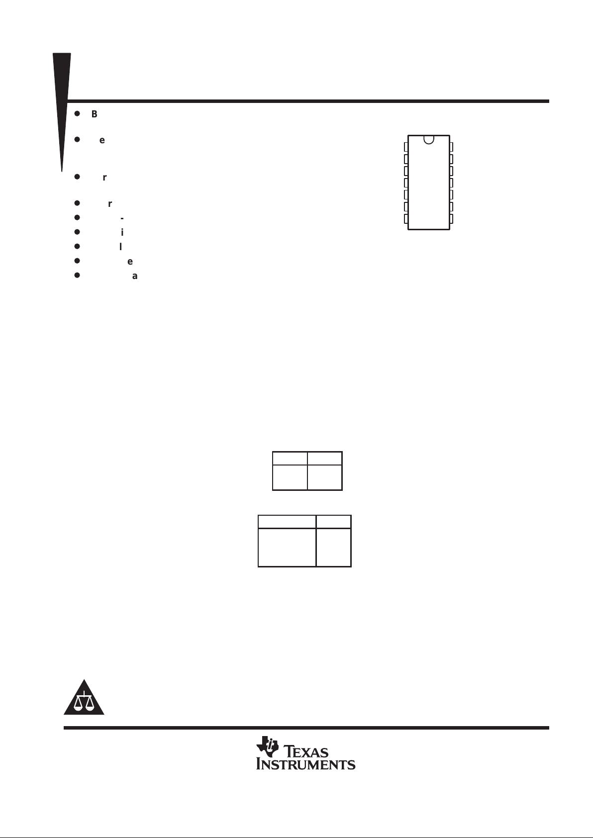
DRIVER 1
B
Y
H L
L H
DRIVERS 2 – 4
A
B Y
H H L
L XH
XLH
H = high level, L = low level,
X = don’t care
Copyright 1997, Texas Instruments Incorporated
PRODUCTION DATA information is current as of publication date.
Products conform to specifications per the terms of Texas Instruments
standard warranty. Production processing does not necessarily include
testing of all parameters.
Please be aware that an important notice concerning availability, standard warranty, and use in critical applications of
Texas Instruments semiconductor products and disclaimers thereto appears at the end of this data sheet.
1
2
3
4
5
6
7
14
13
12
11
10
9
8
V
CC–
1A
1Y
2A
2B
2Y
GND
V
CC+
4B
4A
4Y
3B
3A
3Y
D, DB†, OR N PACKAGE
(TOP VIEW)
†
The DB package is only avalable left-end taped
and reeled, i.e., order device SN75C188DBLE.

SN75C188
QUADRUPLE LOW-POWER LINE DRIVERS
SLLS033F – JANUARY 1988 – REVISED MARCH 1997
2
POST OFFICE BOX 655303 • DALLAS, TEXAS 75265
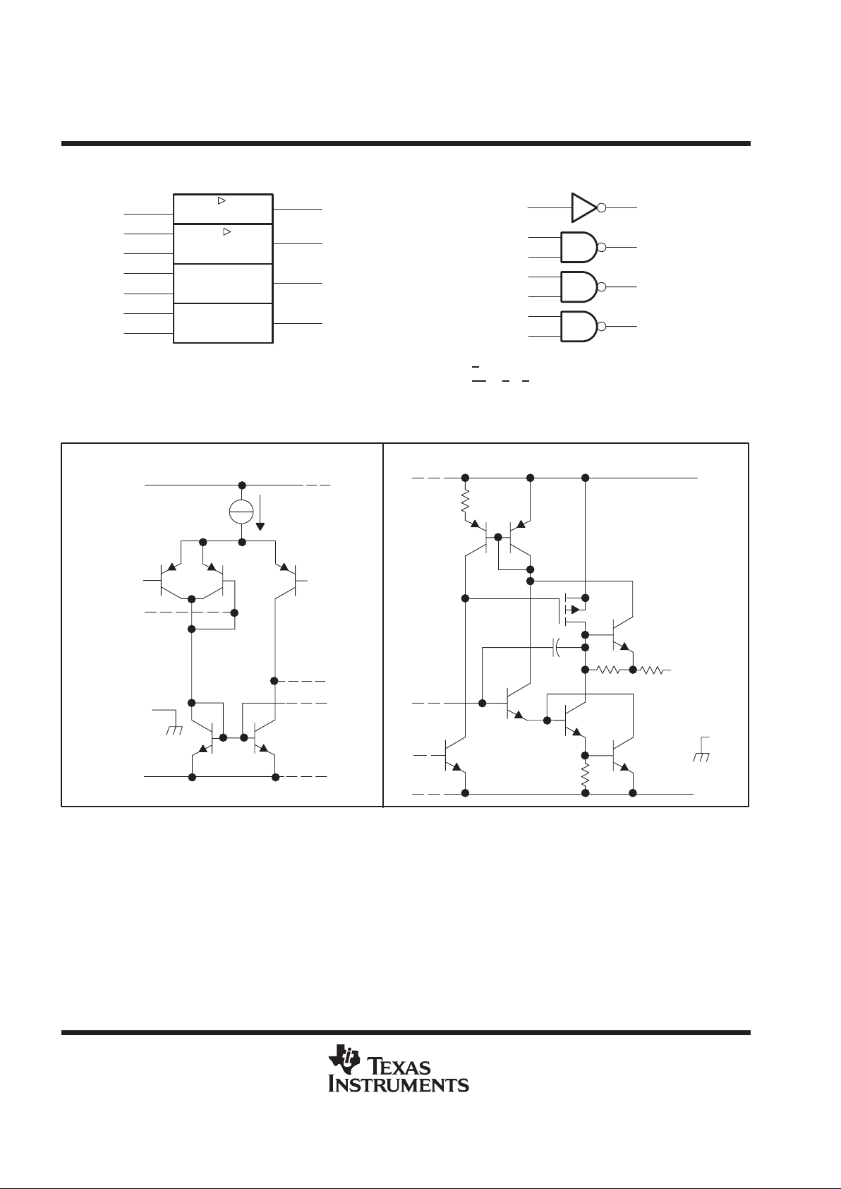
logic symbol
†
4Y
3Y
2Y
1Y
13
12
10
9
5
4
2
4B
4A
3B
3A
2B
2A
1A
11
8
6
3
†
This symbol is in accordance with ANSI/IEEE Std 91-1984
and IEC Publication 617-12.
&
logic diagram (positive logic)
4Y
3Y
2Y
1Y
13
12
10
9
5
4
2
4B
4A
3B
3A
2B
2A
1A
11
8
6
3
positive logic
Y = A
(driver 1)
Y = AB
or A + B (drivers 2 through 4)
schematics of inputs and outputs
EACH OUTPUT
‡
GND
V
CC–
74 Ω
160 Ω
72 Ω
Output
V
CC+
(driver 1 only)
Internal
1.4-V Ref
to GND
V
CC+
Input A
Input B
(drivers 2, 3
and 4 only)
GND
V
CC–
EACH INPUT
‡
All resistor values shown are nominal.

SN75C188
QUADRUPLE LOW-POWER LINE DRIVERS
SLLS033F – JANUARY 1988 – REVISED MARCH 1997
3
POST OFFICE BOX 655303 • DALLAS, TEXAS 75265
absolute maximum ratings over operating free-air temperature range (unless otherwise noted)
†
Supply voltage, V
CC+
(see Note 1) 15 V. . . . . . . . . . . . . . . . . . . . . . . . . . . . . . . . . . . . . . . . . . . . . . . . . . . . . . . . . . .
Supply voltage, V
CC–
(see Note 1) –15 V. . . . . . . . . . . . . . . . . . . . . . . . . . . . . . . . . . . . . . . . . . . . . . . . . . . . . . . . . .
Input voltage range, V
I
V
CC–
to V
CC+
. . . . . . . . . . . . . . . . . . . . . . . . . . . . . . . . . . . . . . . . . . . . . . . . . . . . . . . . . . . . .
Output voltage range, V
O
V
CC–
–6 V to V
CC+
+6 V. . . . . . . . . . . . . . . . . . . . . . . . . . . . . . . . . . . . . . . . . . . . . . . .
Continuous total power dissipation See Dissipation Rating Table. . . . . . . . . . . . . . . . . . . . . . . . . . . . . . . . . . . . .
Operating free-air temperature range, T
A
0°C to 70°C. . . . . . . . . . . . . . . . . . . . . . . . . . . . . . . . . . . . . . . . . . . . . .
Storage temperature range, T
stg
–65°C to 150°C. . . . . . . . . . . . . . . . . . . . . . . . . . . . . . . . . . . . . . . . . . . . . . . . . . .
Lead temperature 1,6 mm (1/16 inch) from case for 10 seconds 260°C. . . . . . . . . . . . . . . . . . . . . . . . . . . . . . .
†
Stresses beyond those listed under “absolute maximum ratings” may cause permanent damage to the device. These are stress ratings only, and
functional operation of the device at these or any other conditions beyond those indicated under “recommended operating conditions” is not
implied. Exposure to absolute-maximum-rated conditions for extended periods may affect device reliability.
NOTE 1: All voltage values are with respect to the network ground terminal.
DISSIPATION RATING TABLE
T
≤ 25°C DERATING FACTOR T
= 70°C
PACKAGE
A
POWER RATING ABOVE TA = 25°C
A
POWER RATING
D 950 mW 7.6 mW/°C 608 mW
DB 525 mW 4.2 mW/°C 336 mW
N 1150 mW 9.2 mW/°C 736 mW
recommended operating conditions
MIN NOM MAX UNIT
Supply voltage, V
CC+
4.5 12 15 V
Supply voltage, V
CC–
–4.5 –12 –15 V
Input voltage, V
I
V
CC–
+2 V
CC+
V
High-level Input voltage, V
IH
2 V
Low-level Input voltage, V
IL
0.8 V
Operating free-air temperature, T
A
0 70 °C
 Loading...