SN75ALS174A
QUADRUPLE DIFFERENTIAL LINE DRIVER
SLLS122E – JULY 1991 – REVISED APRIL 1998
1
POST OFFICE BOX 655303 • DALLAS, TEXAS 75265
D
Meets or Exceeds the Requirements of
ANSI EIA/TIA-422-B and RS-485
D
High-Speed Advanced Low-Power Schottky
Circuitry
D
Designed for up to 20-Mbit/s Operation in
Both Serial and Parallel Applications
D
Designed for Multipoint Transmission on
Long Bus Lines in Noisy Environments
D
Low Supply Current Requirements
55 mA Max
D
Wide Positive and Negative Input/Output
Bus Voltage Ranges
D
Driver Output Capacity...±60 mA
D
Thermal-Shutdown Protection
D
Driver Positive- and Negative-Current
Limiting
D
Functionally Interchangeable With SN75174
description
The SN75ALS174A is a quadruple line driver with
3-state differential outputs. It is designed to meet
the requirements of ANSI Standards
EIA/TIA-422-B and RS-485. This device is
optimized for balanced multipoint bus
transmission at rates of up to 20 Mbit/s. Each
driver features wide positive and negative
common-mode output voltage ranges that make
them suitable for party-line applications in noisy
environments.
The SN75ALS174A provides positive- and negative-current limiting and thermal shutdown for protection from
line fault conditions on the transmission bus line. Shutdown occurs at a junction temperature of
approximately 150°C.
The SN75ALS174A is characterized for operation from 0°C to 70°C.
FUNCTION TABLE
(each driver)
INPUT
OUTPUTS
A
ENABLES
Y Z
H H H L
L H L H
X L Z Z
H = high level, L = low level, X = irrelevant,
Z = high impedance (off)
Copyright 1998, Texas Instruments Incorporated
PRODUCTION DATA information is current as of publication date.
Products conform to specifications per the terms of Texas Instruments
standard warranty. Production processing does not necessarily include
testing of all parameters.
Please be aware that an important notice concerning availability, standard warranty, and use in critical applications of
Texas Instruments semiconductor products and disclaimers thereto appears at the end of this data sheet.
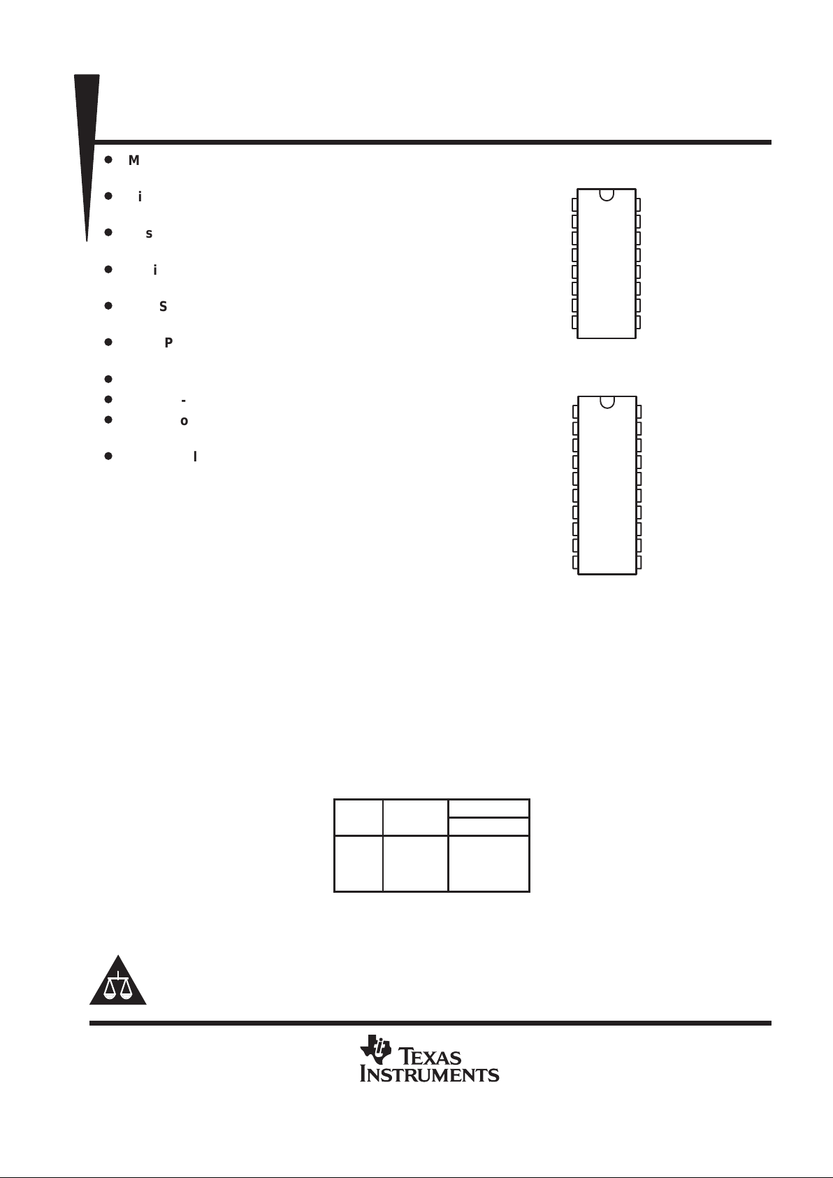
DW PACKAGE
(TOP VIEW)
1
2
3
4
5
6
7
8
9
10
20
19
18
17
16
15
14
13
12
11
1A
1Y
NC
1Z
1,2EN
2Z
NC
2Y
2A
GND
V
CC
4A
4Y
NC
4Z
3,4EN
3Z
NC
3Y
3A
1
2
3
4
5
6
7
8
16
15
14
13
12
11
10
9
1A
1Y
1Z
1,2EN
2Z
2Y
2A
GND
V
CC
4A
4Y
4Z
3,4EN
3Z
3Y
3A
N PACKAGE
(TOP VIEW)
NC – No internal connection

SN75ALS174A
QUADRUPLE DIFFERENTIAL LINE DRIVER
SLLS122E – JULY 1991 – REVISED APRIL 1998
2
POST OFFICE BOX 655303 • DALLAS, TEXAS 75265
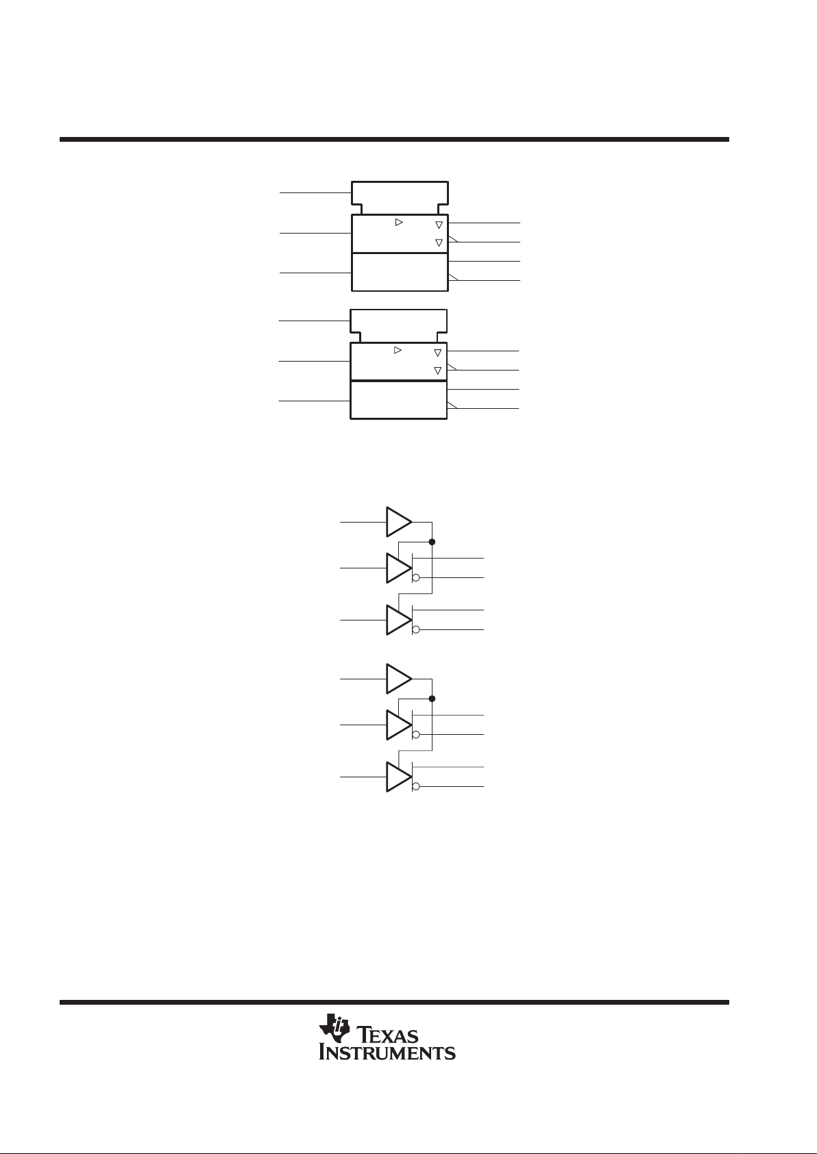
logic symbol
†
1Y
2
1Z
3
2Y
6
2Z
5
1
1A
7
2A
EN
4
1,2EN
3Y
10
3Z
11
4Y
14
4Z
13
9
3A
15
4A
EN
12
3,4EN
†
This symbol is in accordance with ANSI/IEEE Std 91-1984 and IEC Publication 617-12.
Pin numbers shown are for the N package.
logic diagram (positive logic)
Pin numbers shown are for the N package.
4
1
7
2
3
6
5
1,2EN
1A
2A
1Y
1Z
2Y
2Z
12
9
15
10
11
14
13
3,4EN
3A
4A
3Y
3Z
4Y
4Z

SN75ALS174A
QUADRUPLE DIFFERENTIAL LINE DRIVER
SLLS122E – JULY 1991 – REVISED APRIL 1998
3
POST OFFICE BOX 655303 • DALLAS, TEXAS 75265
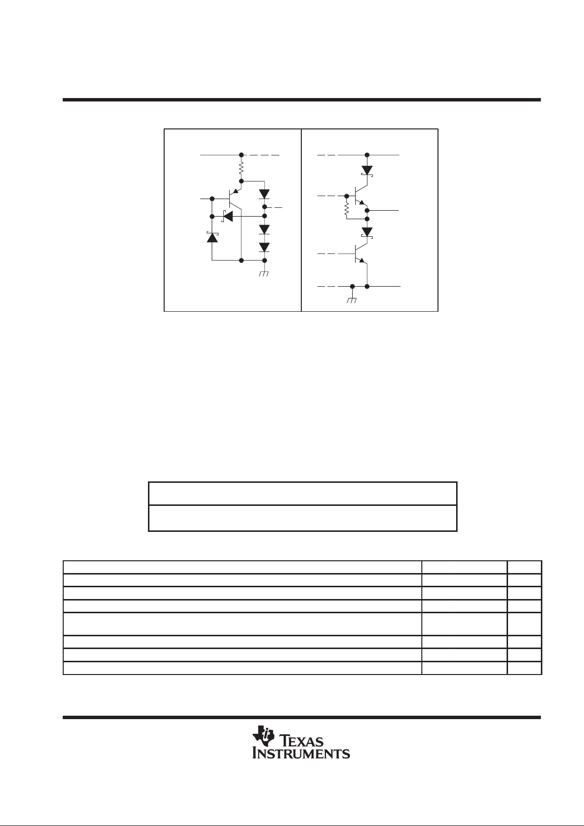
schematics of inputs and outputs
Input
V
CC
Output
GND
V
CC
EQUIVALENT OF EACH INPUT TYPICAL OF ALL OUTPUTS
35 kΩ NOM
absolute maximum ratings over operating free-air temperature range (unless otherwise noted)
†
Supply voltage, V
CC
(see Note 1) 7 V. . . . . . . . . . . . . . . . . . . . . . . . . . . . . . . . . . . . . . . . . . . . . . . . . . . . . . . . . . . . .
Input voltage, V
I
7 V. . . . . . . . . . . . . . . . . . . . . . . . . . . . . . . . . . . . . . . . . . . . . . . . . . . . . . . . . . . . . . . . . . . . . . . . . . . .
Output voltage range, V
O
–9 V to 14 V. . . . . . . . . . . . . . . . . . . . . . . . . . . . . . . . . . . . . . . . . . . . . . . . . . . . . . . . . . . .
Continuous total dissipation See Dissipation Rating Table. . . . . . . . . . . . . . . . . . . . . . . . . . . . . . . . . . . . . . . . . . .
Storage temperature range, T
stg
–65°C to 150°C. . . . . . . . . . . . . . . . . . . . . . . . . . . . . . . . . . . . . . . . . . . . . . . . . . .
Lead temperature 1,6 mm (1/16 inch) from case for 10 seconds 260°C. . . . . . . . . . . . . . . . . . . . . . . . . . . . . . .
†
Stresses beyond those listed under “absolute maximum ratings” may cause permanent damage to the device. These are stress ratings only, and
functional operation of the device at these or any other conditions beyond those indicated under “recommended operating conditions” is not
implied. Exposure to absolute-maximum-rated conditions for extended periods may affect device reliability.
NOTE 1: All voltage values are with respect to network GND.
DISSIPATION RATING TABLE
PACKAGE
TA ≤ 25°C
POWER RATING
DERATING
FACTOR
TA = 70°C
POWER RATING
TA = 85°C
POWER RATING
DW 1125 mW 9.0 mW/°C 720 mW 585 mW
N 1150 mW 9.2 mW/°C 736 mW 598 mW
recommended operating conditions
MIN NOM MAX UNIT
Supply voltage, V
CC
4.75 5 5.25 V
High-level input voltage, V
IH
2 V
Low-level input voltage, V
IL
0.8 V
Common-mode output voltage, V
OC
12
–7
V
High-level output current, I
OH
–60 mA
Low-level output current, I
OL
60 mA
Operating free-air temperature, T
A
0 70 °C
 Loading...