

Texas Instruments SN75ALS171ADW, SN75ALS171ADWR, SN75ALS171DW, SN75ALS171DWR, SN75ALS171J Datasheet
SN75ALS171, SN75ALS171A
TRIPLE DIFFERENTIAL BUS TRANSCEIVERS
SLLS056D – AUGUST 1987 – REVISED SEPTEMBER 1995
D
Three Bidirectional Transceivers
D
Driver Meets or Exceeds the Requirements
of ANSI EIA/TIA-422-B and RS-485 and ITU
Recommendation V.11
D
Two Skew Limits Available
D
Designed to Operate Up to 20 Million Data
Transfers per Second (FAST-20 SCSI)
D
High-Speed Advanced Low-Power Schottky
Circuitry
D
Low Pulse Skew...5 ns Max
D
Designed for Multipoint Transmission on
Long Bus Lines in Noisy Environments
D
Features Independent Driver Enables and
Combined Receiver Enables
D
Wide Positive and Negative Input/Output
Bus Voltages Ranges
D
Driver Output Capacity...±60 mA
D
Thermal Shutdown Protection
D
Driver Positive- and Negative-Current
Limiting
D
Receiver Input Impedances...12 kΩ Min
D
Receiver Input Sensitivity...±300 mV Max
D
Receiver Input Hysteresis...60 mV Typ
D
Operates From a Single 5-V Supply
D
Glitch-Free Power-Up and Power-Down
Protection
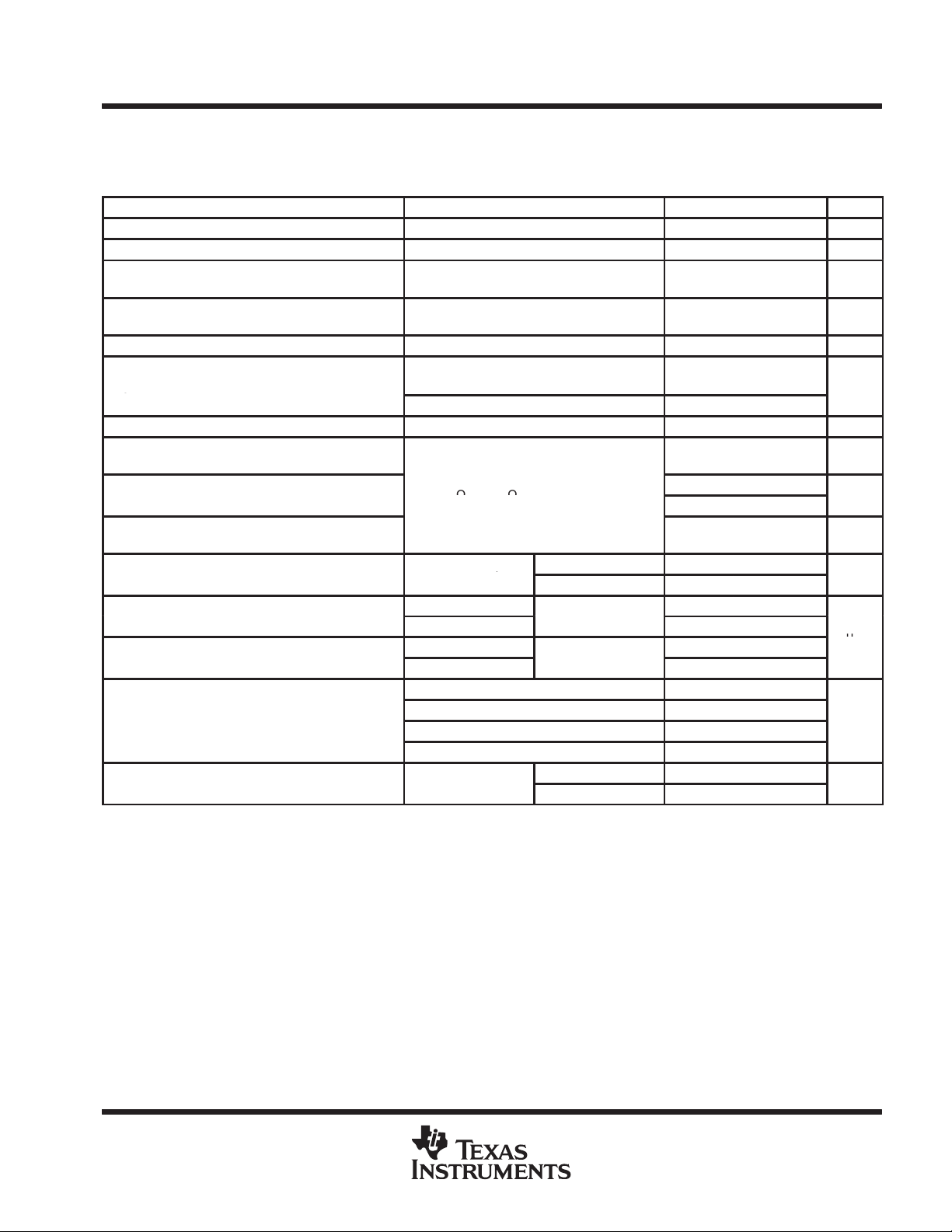
description
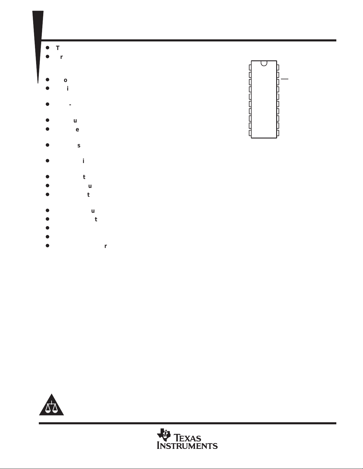
DW OR J PACKAGE
(TOP VIEW)
1R
1
1DE
2
1D
3
GND
GND
2R
2DE
2D
3R
3DE
4
5
6
7
8
9
10
20
19
18
17
16
15
14
13
12
11
1B
1A
RE
CDE
V
CC
2B
2A
3B
3A
3D
The SN75ALS171 and the SN75ALS171A triple differential bus transceivers are monolithic integrated circuits
designed for bidirectional data communication on multipoint bus transmission lines. They are designed for
balanced transmission lines, and each driver meets ANSI Standards EIA/TIA-422-B and RS-485 and both the
drivers and receivers meet ITU Recommendation V .1 1. The SN75ALS171A is designed for F AST -20 SCSI and
can transmit or receive data pulses as short as 30 ns with a maximum skew of 5 ns.
The SN75ALS171 and the SN75ALS171A operate from a single 5-V power supply . The drivers and receivers
have individual active-high and active-low enables, respectively, which can be externally connected together
to function as a direction control. The driver differential output and the receiver differential input pairs are
connected internally to form differential input/output (I/O) bus ports that are designed to offer minimum loading
to the bus when the driver is disabled or V
is at 0 V. These ports feature wide positive and negative
CC
common-mode voltage ranges making the device suitable for party-line applications.
The SN75ALS171 and the SN75ALS171A are characterized for operation from 0°C to 70°C.
Please be aware that an important notice concerning availability, standard warranty, and use in critical applications of
Texas Instruments semiconductor products and disclaimers thereto appears at the end of this data sheet.
PRODUCTION DATA information is current as of publication date.
Products conform to specifications per the terms of Texas Instruments
standard warranty. Production processing does not necessarily include
testing of all parameters.
Copyright 1995, Texas Instruments Incorporated
POST OFFICE BOX 655303 • DALLAS, TEXAS 75265
1
SN75ALS171, SN75ALS171A
TRIPLE DIFFERENTIAL BUS TRANSCEIVERS
SLLS056D – AUGUST 1987 – REVISED SEPTEMBER 1995
Function Tables
EACH DRIVER
INPUT
D
H H H H L
L H HLH
XLXZZ
XXLZZ
DIFFERENTIAL INPUTS
VID ≥ 0.3 V L H
–0.3 V < VID < 0.3 V L ?
VID ≤ –0.3 V L L
H = high level, L = low level, ? = indeterminate, X = irrelevant,
Z = high impedance (off)
ENABLES OUTPUTS
DE CDE A B
EACH RECEIVER
A–B RE R
X H Z
Open L H
ENABLE OUTPUT
AVAILABLE OPTIONS
SKEW LIMIT
10 ns SN75ALS171DW SN75ALS171J
5 ns SN75ALS171ADW
PART NUMBER
2
POST OFFICE BOX 655303 • DALLAS, TEXAS 75265
SN75ALS171, SN75ALS171A
TRIPLE DIFFERENTIAL BUS TRANSCEIVERS
SLLS056D – AUGUST 1987 – REVISED SEPTEMBER 1995
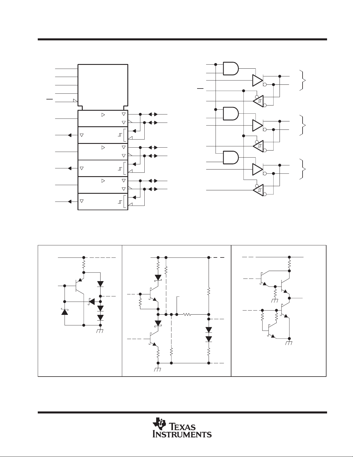
logic symbol
17
CDE
2
1DE
7
2DE
10
3DE
18
RE
3
1D
1
1R
8
2D
6
2R
11
3D
9
3R
†
G5
5EN1
5EN2
5EN3
EN4
logic diagram (positive logic)
17
CDE
2
1DE
3
1D
18
RE
1
1R
1
1
1
4
2
2
1
4
3
3
1
4
19
20
14
15
12
13
1A
1B
2A
2B
3A
3B
2DE
2D
2R
3DE
3D
3R
7
8
6
10
11
9
19
20
14
15
12
13
1A
1B
2A
2B
3A
3B
Bus
Bus
Bus
†
This symbol is in accordance with ANSI/IEEE Std 91-1984 and
IEC Publication 617-12.
schematics of inputs and outputs
EQUIVALENT OF EACH INPUT
V
CC
R
(eq)
Input
Driver Input: R
Enable Inputs: R
R
= equivalent resistor
(eq)
= 12 kΩ NOM
(eq)
= 8 kΩ
(eq)
NOM
TYPICAL OF A AND B I/O PORTS TYPICAL OF RECEIVER OUTPUT
V
CC
180 kΩ
NOM
Connected
on A Port
A or B
18 kΩ
NOM
180 kΩ
NOM
Connected
on B Port
3 kΩ
NOM
1.1 kΩ
NOM
85 Ω
NOM
V
CC
Output
POST OFFICE BOX 655303 • DALLAS, TEXAS 75265
3
SN75ALS171, SN75ALS171A
High-level output current, I
Low-level output current, I
mA
TRIPLE DIFFERENTIAL BUS TRANSCEIVERS
SLLS056D – AUGUST 1987 – REVISED SEPTEMBER 1995
absolute maximum ratings over operating free-air temperature range (unless otherwise noted)
Supply voltage, V
Voltage range at any bus terminal –7 V to 12 V. . . . . . . . . . . . . . . . . . . . . . . . . . . . . . . . . . . . . . . . . . . . . . . . . . . . .
Enable input voltage, V
Continuous total power dissipation See Dissipation Rating Table. . . . . . . . . . . . . . . . . . . . . . . . . . . . . . . . . . . . .
Operating free-air temperature range, T
Storage temperature range, T
Lead temperature 1,6 mm (1/16 inch) from case for 10 seconds: DW package 260°C. . . . . . . . . . . . . . . . . .
Lead temperature 1,6 mm (1/16 inch) from case for 60 seconds: J package 300°C. . . . . . . . . . . . . . . . . . . . .
†
Stresses beyond those listed under “absolute maximum ratings” may cause permanent damage to the device. These are stress ratings only, and
functional operation of the device at these or any other conditions beyond those indicated under “recommended operating conditions” is not
implied. Exposure to absolute-maximum-rated conditions for extended periods may affect device reliability.
NOTE 1: All voltage values, except differential I/O bus voltage, are with respect to network ground terminal.
(see Note 1) 7 V. . . . . . . . . . . . . . . . . . . . . . . . . . . . . . . . . . . . . . . . . . . . . . . . . . . . . . . . . . . . .
CC
7 V. . . . . . . . . . . . . . . . . . . . . . . . . . . . . . . . . . . . . . . . . . . . . . . . . . . . . . . . . . . . . . . . . . . . . .
I
0°C to 70°C. . . . . . . . . . . . . . . . . . . . . . . . . . . . . . . . . . . . . . . . . . . . . .
–65°C to 150°C. . . . . . . . . . . . . . . . . . . . . . . . . . . . . . . . . . . . . . . . . . . . . . . . . . .
stg
PACKAGE
DW 1125 mW 9.0 mW/°C 720 mW
J 1025 mW 8.2 mW/°C 656 mW
POWER RATING
A
DISSIPATION RATING TABLE
TA ≤ 25°C
DERATING FACTOR
ABOVE TA = 25°C
TA = 70°C
POWER RATING
recommended operating conditions
MIN NOM MAX UNIT
Supply voltage, V
Voltage at any bus terminal (separately or common mode), VI or V
High-level input voltage, V
Low-level input voltage, V
Differential input voltage, VID (see Note 2) ±12 V
Operating free-air temperature, T
NOTE 2: Differential-input/output bus voltage is measured at the noninverting terminal A with respect to the inverting terminal B.
CC
IC
IH
IL
p
p
OH
OL
A
D, CDE, DE, and RE 2 V
D, CDE, DE, and RE 0.8 V
Driver –60 mA
Receiver –400 µA
Driver 60
Receiver 8
4.75 5 5.25 V
–7 12 V
0 70 °C
†
4
POST OFFICE BOX 655303 • DALLAS, TEXAS 75265
OD2
g
VOCCommon-mode output voltage
R
54 Ω or 100 Ω
See Figure 1
V
IOOutput current
,
mA
IIHHigh-level enable-input current
V
V
A
IILLow-level enable-input current
V
0.4 V
I
Short-ci
t
mA
ICCSupply current
No load
mA
SN75ALS171, SN75ALS171A
TRIPLE DIFFERENTIAL BUS TRANSCEIVERS
SLLS056D – AUGUST 1987 – REVISED SEPTEMBER 1995
DRIVER SECTION
electrical characteristics over recommended ranges of supply voltage and operating free-air
temperature (unless otherwise noted)
IH
=
IL
= 2.7
†
MIN TYP‡MAX UNIT
2.7 V
1.7 V
1/2V
or 2
OD1
§
2.5 5
±0.2 V
3
–1
±0.2 V
20
60
–100
–900
250
V
µ
PARAMETER TEST CONDITIONS
V
IK
V
O
V
OH
V
OL
|V
OD1
|V
OD2
V
OD3
∆|VOD|
∆|VOC|
OS
†
The power-off measurement in ANSI Standard EIA/TIA-422-B applies to disabled outputs only and is not applied to combined inputs and outputs.
‡
All typical values are at VCC = 5 V and TA = 25°C.
§
The minimum V
¶
∆|VOD| and ∆|VOC| are the changes in magnitude of VOD and VOC, respectively, that occur when the input is changed from a high level to a
low level.
NOTE 3: This applies for both power on and off; refer to EIA Standard RS-485 for exact conditions. The EIA/TIA-422-B limit does not apply for
Input clamp voltage II = –18 mA –1.5 V
Output voltage IO = 0 0 6 V
High-level output voltage
Low-level output voltage
| Differential output voltage IO = 0 1.5 6 V
| Differential output voltage
Differential output voltage V
Change in magnitude of differential
output voltage
Change in magnitude of common-mode
output voltage
p
pp
OD2
a combined driver and receiver terminal.
¶
p
¶
p
p
rcuit output curren
with 100-W load is either 1/2 V
VCC = 4.75 V,
VIL = 0.8 V,
VCC = 4.75 V,
VIL = 0.8 V,
RL = 100 Ω, See Figure 1
RL = 54 Ω, See Figure 1 1.5 2.5 5
= –7 V to 12 V , See Figure 2 1.5 5 V
test
=
L
Output disabled,
See Note 3
D and DE
CDE
D and DE
CDE
VO = –6 V –250
VO = 0 –150
VO = V
CC
VO = 8 V 250
or 2 V, whichever is greater.
OD2
VIH = 2 V,
IOH = –55 mA
VIH = 2 V,
IOL = 55 mA
,
VO = 12 V 1
VO = –7 V –0.8
Outputs enabled 69 90
Outputs disabled 57 78
POST OFFICE BOX 655303 • DALLAS, TEXAS 75265
5
SN75ALS171, SN75ALS171A
L
,
g,
C
60 pF
See Figure 6
t
Pul
‡
L
,
L
,
t
Sk
it
§
ns
L1 L3
,
L2
,
L1 L3
L2
TRIPLE DIFFERENTIAL BUS TRANSCEIVERS
SLLS056D – AUGUST 1987 – REVISED SEPTEMBER 1995
switching characteristics over recommended ranges of supply voltage and operating free-air
temperature (unless otherwise noted)
PARAMETER TEST CONDITIONS MIN TYP†MAX UNIT
ALS171
ALS171A
t
d(OD)
sk(p)
sk(lim)
t
t(OD)
t
PZH
t
PZL
t
PHZ
t
PLZ
t
PDE
t
PDZ
†
All typical values are at VCC = 5 V and TA = 25°C.
‡
Pulse skew is defined as the |t
§
Skew limit is the maximum difference in propagation delay times between any two channels of one device and between any two devices. This
parameter is applicable at one VCC and operating temperature within the recommended operating conditions.
Differential output delay time
se skew
ew lim
Differential-output transition time
Output enable time to high level RL = 110 Ω, See Figure 4 30 50 ns
Output enable time to low level RL = 110 Ω, See Figure 5 30 50 ns
Output disable time from high level RL = 110 Ω, See Figure 4 3 8 13 ns
Output disable time from low level RL = 110 Ω, See Figure 5 3 8 13 ns
Differential-output enable time
Differential-output disable time
– t
d(ODH)
| of each channel.
d(ODL)
ALS171
ALS171A
ALS171
ALS171A
ALS171
ALS171A
R
= 54 Ω, See Figure 3,
CL = 50 pF
RL1 = RL3 = 165 Ω,pV
,
=
L
RL2 = 75 Ω,
RL = 54 Ω,
See Figure 3
RL1 = RL3 = 165 Ω,
CL = 60 pF,
R
= 54 Ω, C
See Figure 3
R
= R
= 165 Ω, R
CL = 60 pF,
RL = 54 Ω,
See Figure 3
RL1 = RL3 = 165 Ω,
CL = 60 pF,
See Figure 6
RL1 = RL3 = 165 Ω, RL2 = 75 Ω,
CL = 60 pF,
= 5 V,
TERM
CL = 50 pF,
RL2 = 75 Ω,
See Figure 6
= 50 pF,
= 75 Ω,
See Figure 6
CL = 50 pF,
RL2 = 75 Ω,
V
= 5 V,
TERM
See Figure 7
3 13
6 11
3 13
6 11
1 5 ns
1 5 ns
3 8 13
3 8 13
8 30 45 ns
5 10 45 ns
ns
10
5
10
5
ns
SYMBOL EQUIVALENTS
DATA-SHEET PARAMETER
V
O
|V
| V
OD1
|V
| Vt (RL = 100 Ω) Vt (RL = 54 Ω)
OD2
|V
|
OD3
V
test
∆|VOD| ||Vt|–|V
V
OC
∆|VOC| |Vos –Vos| |Vos –Vos|
I
OS
I
O
6
POST OFFICE BOX 655303 • DALLAS, TEXAS 75265
EIA/TIA-422-B RS-485
Voa, V
ob
o
||
t
|Vos| |Vos|
|Isa|, |Isb|
|Ixa|, |Ixb| Iia, I
Voa, V
V
o
Vt (Test Termination
Measurement 2)
V
tst
||Vt|–|V
ib
ob
||
t
 Loading...