

Page 1
SN75ALS170, SN75ALS170A
TRIPLE DIFFERENTIAL BUS TRANSCEIVER
SLLS055D – AUGUST 1987 – REVISED SEPTEMBER 1995
D
Three Bidirectional Transceivers
D
Driver Meets or Exceeds ANSI Standard
EIA/TIA-422-B and RS-485 and ITU
Recommendation V.11
D
Two Skew Limits Available
D
Designed to Operate Up to 20 Million Data
Transfers per Second (FAST-20 SCSI)
D
High-Speed Advanced Low-Power Schottky
Circuitry
D
Designed for Multipoint Transmission on
Long Bus Lines in Noisy Environments
D
Wide Positive and Negative Input/Output
Bus Voltage Ranges
D
Driver Output Capacity...±60 mA
D
Thermal Shutdown Protection
D
Driver Positive- and Negative-Current
Limiting
D
Receiver Input Impedances...12 kΩ Min
D
Receiver Input Sensitivity...±300 mV Max
D
Receiver Input Hysteresis...60 mV Typ
D
Operate From a Single 5-V Supply
D
Glitch-Free Power-Up and Power-Down
Protection
D
Feature Independent Direction Controls for
Each Channel
description
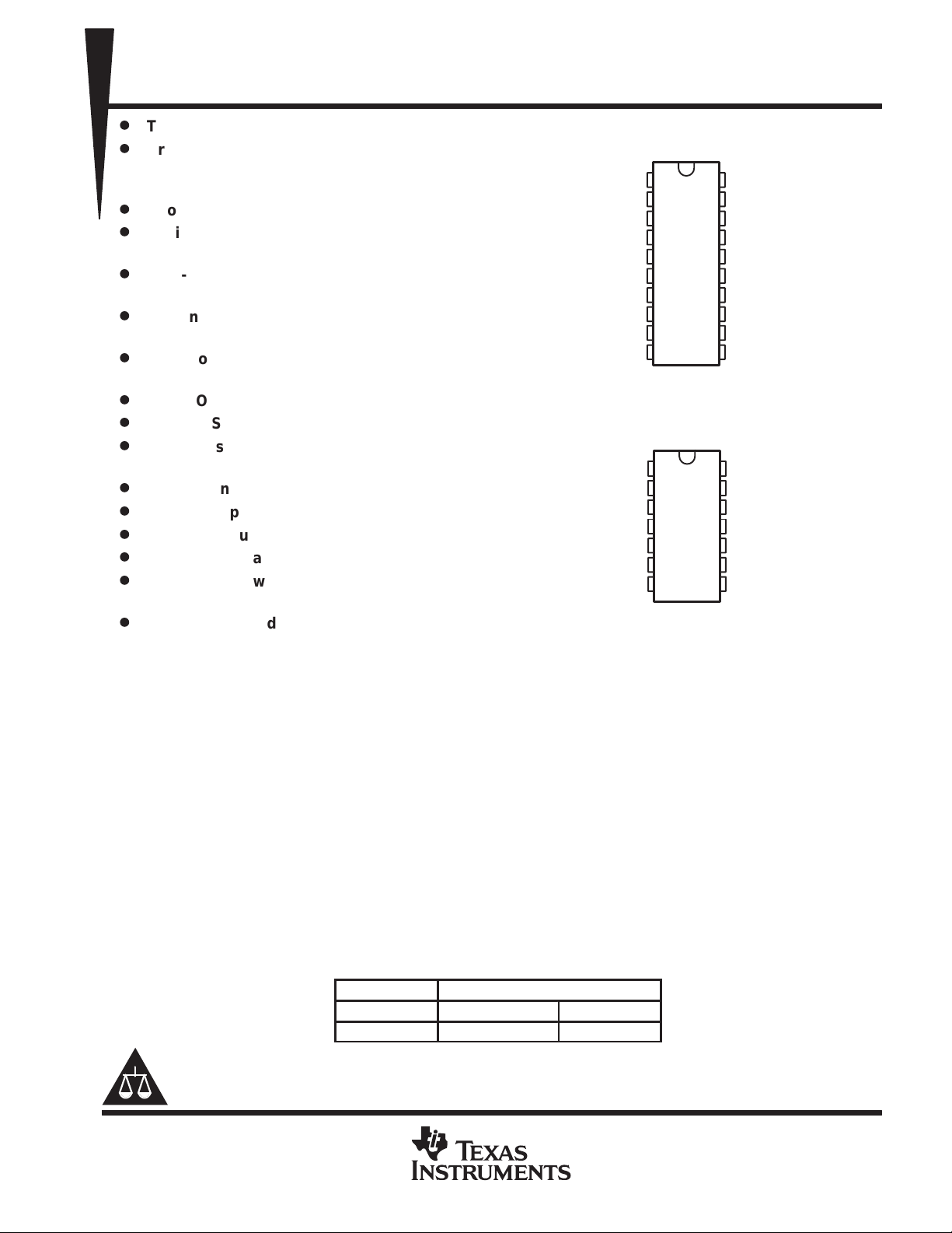
DW PACKAGE
(TOP VIEW)
1D
1
1DIR
GND
2DIR
3DIR
NC – No internal connection
1DIR
GND
2DIR
3DIR
NC
NC
2D
NC
3D
1D
2D
3D
2
3
4
5
6
7
8
9
10
J PACKAGE
(TOP VIEW)
1
2
3
4
5
6
7
20
19
18
17
16
15
14
13
12
11
14
13
12
10
1B
1A
NC
NC
V
CC
2B
2A
3B
3A
NC
1B
1A
V
CC
2B
11
2A
9
3B
8
3A
The SN75ALS170 and SN75ALS170A triple differential bus transceivers are monolithic integrated circuits
designed for bidirectional data communication on multipoint bus transmission lines. It is designed for balanced
transmission lines and the driver meets ANSI Standards EIA/TIA-422-B and RS-485 and both the driver and
receiver meet ITU Recommendation V .1 1. The SN75ALS170A is designed for F AST -20 SCSI and can transmit
or receive data pulses as short as 30 ns with a maximum skew of 5 ns.
The SN75ALS170 and SN75ALS170A operate from a single 5-V power supply . The drivers and receivers have
active-high and active-low enables, respectively, which are internally connected together to function as a
direction control. The driver differential outputs and the receiver differential inputs are connected internally to
form differential input/output (I/O) bus ports that are designed to offer minimum loading to the bus when the
driver is disabled or V
= 0. These ports feature wide positive and negative common-mode voltage ranges
CC
making the device suitable for party-line applications.
The SN75ALS170 and the SN75ALS170A are characterized for operation from 0°C to 70°C.
AVAILABLE OPTIONS
SKEW LIMIT
Please be aware that an important notice concerning availability, standard warranty, and use in critical applications of
Texas Instruments semiconductor products and disclaimers thereto appears at the end of this data sheet.
PRODUCTION DATA information is current as of publication date.
Products conform to specifications per the terms of Texas Instruments
standard warranty. Production processing does not necessarily include
testing of all parameters.
10 ns SN75ALS170DW SN75ALS170J
5 ns SN75ALS170ADW
PART NUMBER
Copyright 1995, Texas Instruments Incorporated
POST OFFICE BOX 655303 • DALLAS, TEXAS 75265
1
Page 2
SN75ALS170, SN75ALS170A
DIR
DIR
TRIPLE DIFFERENTIAL BUS TRANSCEIVER
SLLS055D – AUGUST 1987 – REVISED SEPTEMBER 1995
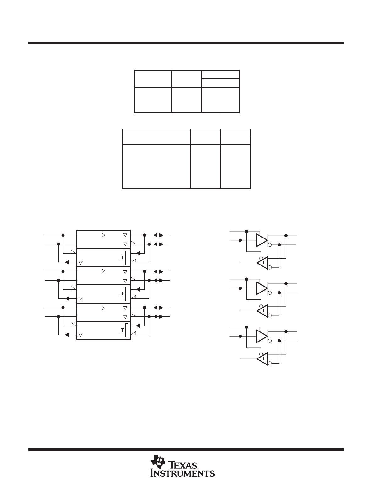
Function Tables
EACH DRIVER
INPUT
D
H H H L
L H L H
X L Z Z
EACH RECEIVER
DIFFERENTIAL INPUTS
A – B
VID ≥ 0.3 V L H
–0.3 V < VID < 0.3 V L ?
VID ≤ – 0.3 V L L
X H Z
Open L H
H = high level, L = low level, ? = indeterminate,
X = irrelevant, Z = high impedance (off)
OUTPUTS
A B
OUTPUT
R
logic symbol
2
1DIR
1
1D
7
2DIR
6
2D
10
3DIR
9
3D
†
This symbol is in accordance with ANSI/IEEE Std 91-1984 and
IEC Publication 617-12.
Pin numbers shown are for the DW package.
†
EN
EN
EN
EN
EN
EN
1
1
1
19
20
14
15
12
13
logic diagram (positive logic)
2
1A
1B
2A
2B
3A
3B
1DIR
1D
2DIR
2D
3DIR
3D
1
7
6
10
9
19
20
14
15
12
13
1A
1B
2A
2B
3A
3B
2
POST OFFICE BOX 655303 • DALLAS, TEXAS 75265
Page 3
PACKAGE
A
A
schematics of inputs and outputs
SN75ALS170, SN75ALS170A
TRIPLE DIFFERENTIAL BUS TRANSCEIVER
SLLS055D – AUGUST 1987 – REVISED SEPTEMBER 1995
EQUIVALENT OF EACH INPUT
V
CC
R
(eq)
Input
Driver Input: R
Enable Inputs: R
R
= equivalent resistor
(eq)
= 12 kΩ NOM
(eq)
= 8 kΩ
(eq)
NOM
TYPICAL OF A AND B I/O PORTS TYPICAL OF RECEIVER OUTPUT
V
CC
180 kΩ
NOM
Connected
on A Port
A or B
18 kΩ
NOM
180 kΩ
NOM
Connected
on B Port
3 kΩ
NOM
1.1 kΩ
NOM
85 Ω
NOM
V
CC
Output
absolute maximum ratings over operating free-air temperature range (unless otherwise noted)
Supply voltage, V
Voltage range at any bus terminal –7 V to 12 V. . . . . . . . . . . . . . . . . . . . . . . . . . . . . . . . . . . . . . . . . . . . . . . . . . . . .
Enable input voltage, V
Continuous total power dissipation See Dissipation Rating Table. . . . . . . . . . . . . . . . . . . . . . . . . . . . . . . . . . . . .
Operating free-air temperature range, T
Storage temperature range, T
Lead temperature 1,6 mm (1/16 inch) from case for 10 seconds: DW package 260°C. . . . . . . . . . . . . . . . . .
Lead temperature 1,6 mm (1/16 inch) from case for 60 seconds: J package 300°C. . . . . . . . . . . . . . . . . . . . .
†
Stresses beyond those listed under “absolute maximum ratings” may cause permanent damage to the device. These are stress ratings only, and
functional operation of the device at these or any other conditions beyond those indicated under “recommended operating conditions” is not
implied. Exposure to absolute-maximum-rated conditions for extended periods may affect device reliability.
NOTE 1: All voltage values, except differential I/O bus voltage, are with respect to network ground terminal.
(see Note 1) 7 V. . . . . . . . . . . . . . . . . . . . . . . . . . . . . . . . . . . . . . . . . . . . . . . . . . . . . . . . . . . . .
CC
5.5 V. . . . . . . . . . . . . . . . . . . . . . . . . . . . . . . . . . . . . . . . . . . . . . . . . . . . . . . . . . . . . . . . . . . .
I
0°C to 70°C. . . . . . . . . . . . . . . . . . . . . . . . . . . . . . . . . . . . . . . . . . . . . .
–65°C to 150°C. . . . . . . . . . . . . . . . . . . . . . . . . . . . . . . . . . . . . . . . . . . . . . . . . . .
stg
A
†
DISSIPATION RATING TABLE
T
≤ 25°C DERATING FACTOR T
POWER RATING ABOVE TA = 25°C
DW 1125 mW 9.0 mW/°C 720 mW
J 1025 mW 8.2 mW/°C 656 mW
POST OFFICE BOX 655303 • DALLAS, TEXAS 75265
= 70°C
POWER RATING
3
Page 4
SN75ALS170, SN75ALS170A
Voltage at any bus terminal (separately or common mode), V
V
V
High-level output current, I
Low-level output current, I
mA
TRIPLE DIFFERENTIAL BUS TRANSCEIVER
SLLS055D – AUGUST 1987 – REVISED SEPTEMBER 1995
recommended operating conditions
MIN TYP MAX UNIT
Supply voltage, V
High-level input voltage, V
Low-level input voltage, V
Differential input voltage, VID (see Note 2) ±12 V
Operating free-air temperature, T
NOTE 2: Differential-input/output bus voltage is measured at the noninverting terminal A with respect to the inverting terminal B.
CC
p
IH
IL
p
p
OH
OL
A
or
I
IC
D, DIR 2 V
D, DIR 0.8 V
Driver –60 mA
Receiver –400 µA
Driver 60
Receiver 8
4.75 5 5.25 V
12
–7
0 70 °C
4
POST OFFICE BOX 655303 • DALLAS, TEXAS 75265
Page 5
V
CC
V
IH
VOHHigh level out ut voltage
V
I
A
2.7
V
OD2
g
VOCCommon-mode output voltage
R
540 Ω
100 Ω
1
V
IOOutput current
,
mA
I
Short-ci
t
mA
ICCSupply current
No load
mA
SN75ALS170, SN75ALS170A
TRIPLE DIFFERENTIAL BUS TRANSCEIVER
SLLS055D – AUGUST 1987 – REVISED SEPTEMBER 1995
DRIVER SECTION
electrical characteristics over recommended ranges of supply voltage and operating free-air
temperature (unless otherwise noted)
PARAMETER TEST CONDITIONS
V
IK
V
O
V
V
OL
| V
OD1
| V
OD2
V
OD3
∆ | VOD |
∆ | VOC |
I
IH
I
IL
OS
†
The power-off measurement in ANSI Standard EIA/TIA-422-B applies to disabled outputs only and is not applied to combined inputs and outputs.
‡
All typical values are at VCC = 5 V and TA = 25°C.
§
The minimum V
¶
∆ | VOD | and ∆ | VOC | are the changes in magnitude of VOD and VOC respectively, that occur when the input is changed from a high level to a
low level.
NOTE 3: This applies for both power on and off; refer to EIA Standard RS-485 for exact conditions. The EIA/TIA-422-B limit does not apply for
Input clamp voltage II = –19 mA –1.5 V
Output voltage IO = 0 0 6 V
High-level output voltage
Low-level output voltage
| Differential output voltage IO = 0 1.5 6 V
| Differential output voltage
Differential output voltage V
Change in magnitude of differential output
¶
voltage
p
Change in magnitude of common-mode
output voltage
p
High-level input current VI = 2.4 V 20 µA
Low-level input current VI = 0.4 V –400 µA
pp
OD2
a combined driver and receiver terminal.
¶
rcuit output curren
with a 100-Ω load is either 1/2 V
or 2 V, whichever is greater.
OD1
= 4.75 V,
= 0.8 V,
IL
VCC = 4.75 V,
VIL = 0.8 V,
RL = 100 Ω, See Figure 1
RL = 54 Ω, See Figure 1 1.5 2.5 5 V
= –7 V to 12 V , See Figure 2 1.5 5 V
test
=
L
Output disabled,
See Note 3
VO = –6 V –250
VO = 0 –150
VO = V
VO = 8 V 250
CC
or
,See Figure
†
= 2 V,
= –55 m
OH
VIH = 2 V,
IOL = 55 mA
VO = 12 V 1
VO = –7 V –0.8
Outputs enabled 69 90
Outputs disabled 57 78
MIN TYP‡MAX UNIT
2.7 V
1.7 V
1/2V
OD1
§
or 2
±0.2 V
–1
±0.2 V
250
V
3
POST OFFICE BOX 655303 • DALLAS, TEXAS 75265
5
Page 6
SN75ALS170, SN75ALS170A
L
,
L
,
C
60 pF
T
25°C
t
Pul
‡
L
,
L
,
t
Skew limit
§
ns
L1 L3
,
L2
,
t
Differential-output transition time
ns
TRIPLE DIFFERENTIAL BUS TRANSCEIVER
SLLS055D – AUGUST 1987 – REVISED SEPTEMBER 1995
switching characteristics over recommended ranges of supply voltage and operating free-air
temperature (unless otherwise noted)
PARAMETER TEST CONDITIONS MIN TYP†MAX UNIT
ALS170
ALS170A
t
d(OD)
sk(p)
sk(lim)
t(OD)
†
All typical values are at VCC = 5 V and TA = 25°C.
‡
Pulse skew is defined as the |t
§
Skew limit is the maximum difference in propagation delay times between any two channels of one device and between any two devices. This
parameter is applicable at one VCC and operating temperature within the recommended operating conditions.
Differential output delay time
se skew
p
d(ODH)–td(ODL)
ALS170
ALS170A
ALS170
ALS170A
ALS170
ALS170A
| of each channel.
R
= 54 Ω, C
TA =25°C,
RL1 = RL3 = 165 Ω,pRL2 = 75 Ω,
,
=
L
See Figure 4
RL = 54 Ω,
See Figure 3
RL1 = RL3 = 165 Ω,
CL = 60 pF,
R
= 54 Ω, C
See Figure 3
R
= R
= 165 Ω, R
CL = 60 pF,
RL = 54 Ω,
See Figure 3
RL1 = RL3 = 165 Ω,
CL = 60 pF,
= 50 pF,
See Figure 3
°
=
A
CL = 50 pF,
RL2 = 75 Ω,
See Figure 4
= 50 pF,
= 75 Ω,
See Figure 4
CL = 50 pF,
RL2 = 75 Ω,
See Figure 4
,
3 8 13
5.5
5.5
8 10.5
3 8 13
8 10.5
1 5 ns
1 5 ns
3 8 13
3 8 13
ns
10
5
10
5
DATA SHEET PARAMETER
V
O
| V
| V
OD1
| VOD2 | Vt (RL = 100 Ω) Vt (RL = 54 Ω)
| V
|
OD3
V
test
∆ | VOD | || Vt | – | Vt || || Vt | – | Vt ||
V
OC
∆ | VOC | | Vos – Vos | | Vos – Vos |
I
OS
I
O
SYMBOL EQUIVALENTS
EIA/TIA-422-B RS-485
Voa, V
ob
O
Vt (Test Termination
| Vos | | Vos |
| Isa |, | Isb |
| Ixa |, | Ixb | Iia, I
Voa, V
ob
V
O
Measurement 2)
V
tst
ib
6
POST OFFICE BOX 655303 • DALLAS, TEXAS 75265
Page 7
IOZHigh-impedance-state output current
A
IILine input current
,
mA
ICCSupply current
No load
mA
t
gy,g
ns
C
15 pF
T
25°C
g
t
gy,g
See Figure 6
ns
t
Pul
§
ns
ID
,
t
k(lim)
Skew limit
¶
ns
SN75ALS170, SN75ALS170A
TRIPLE DIFFERENTIAL BUS TRANSCEIVER
SLLS055D – AUGUST 1987 – REVISED SEPTEMBER 1995
RECEIVER SECTION
electrical characteristics over recommended ranges of common-mode input voltage, supply
voltage, and operating free-air temperature (unless otherwise noted)
PARAMETER TEST CONDITIONS MIN TYP†MAX UNIT
V
IT+
V
IT–
V
hys
V
IK
V
OH
V
OL
I
IH
I
IL
r
I
I
OS
†
All typical values are at VCC = 5 V and TA = 25°C.
‡
The algebraic convention, in which the less-positive (more-negative) limit is designated minimum, is used in this data sheet for common-mode
input voltage and threshold voltage levels only .
NOTE 4: This applies for both power on and off; refer to EIA Standard RS-485 for exact conditions.
Positive-going input threshold voltage VO = 2.7 V, IO = –0.4 mA 0.3 V
Negative-going input threshold voltage VO = 0.5 V, IO = 8 mA –0.3
Hysteresis voltage (V
Enable-input clamp voltage II = –18 mA –1.5 V
High-level output voltage
Low-level output voltage
p
p
High-level enable-input current VIH = 2.7 V 20 µA
Low-level enable-input current VIL = 0.4 V –100 µA
Input resistance 12 kΩ
Short-circuit output current VID = 300 mV, VO = 0 –15 –85 mA
pp
IT+
– V
) 60 mV
IT–
VID = 300 mV,
See Figure 5
VID = –300 mV,
See Figure 5
p
VO = 2.4 V 20
VO = 0.4 V –400
Other input = 0,
See Note 4
IOH = –400 µA,
IOL = 8 mA,
VI = 12 V 1
VI = –7 V –0.8
Outputs enabled 69 90
Outputs disabled 57 78
‡
2.7 V
0.45 V
V
µ
switching characteristics over recommended ranges of supply voltage and operating free-air
temperature range
PARAMETER TEST CONDITIONS MIN TYP†MAX UNIT
PLH
PHL
sk(p)
s
†
All typical values are at VCC = 5 V and TA = 25°C.
§
Pulse skew is defined as the |t
¶
Skew limit is the maximum difference in propagation delay times between any two channels of one device and between any two devices. This
parameter is applicable at one VCC and operating temperature within the recommended operating conditions.
Propagation delay time, low-to-high-level
output
Propagation delay time, high-to-low-level
output
se skew
PLH–tPHL
| of each channel.
ALS170 9 19
ALS170A
ALS170
ALS170A
ALS170 2 6
ALS170A
ALS170
ALS170A 5
VID = –1.5 V to 1.5 V ,
L
ure 6
See Fi
V
= –1.5 V to 1.5 V ,
CL = 15 pF, See Figure 6
A
,
=
p
=
,
°
11.5 16.5
9 19
11.5 16.5
10
5
POST OFFICE BOX 655303 • DALLAS, TEXAS 75265
7
Page 8

SN75ALS170, SN75ALS170A
TRIPLE DIFFERENTIAL BUS TRANSCEIVER
SLLS055D – AUGUST 1987 – REVISED SEPTEMBER 1995
PARAMETER MEASUREMENT INFORMATION
V
OD2
R
L
2
R
L
V
OC
2
Figure 1. Driver VOD and V
375 Ω
V
OD3
60 Ω
375 Ω
Figure 2. Driver V
CL= 50 pF
RL = 54 Ω
Generator
(see Note A)
NOTES: A. The input pulse is supplied by a generator having the following characteristics: PRR ≤ 1 MHz, 50% duty cycle, tr ≤ 6 ns, tf ≤ 6 ns,
ZO = 50 Ω.
B. CL includes probe and jig capacitance.
50 Ω
3 V
TEST CIRCUIT VOLTAGE WAVEFORMS
(see Note B)
Output
OD3
OC
Input
t
d(ODH)
Output
V
test
t
t(OD)
50%
10%
1.5 V
3 V
1.5 V
0 V
t
d(ODL)
50%
10%
≈ 2.5 V
≈ – 2.5 V
t
t(OD)
90%90%
Figure 3. Driver Test Circuit and Voltage Waveforms
8
POST OFFICE BOX 655303 • DALLAS, TEXAS 75265
Page 9

SN75ALS170, SN75ALS170A
TRIPLE DIFFERENTIAL BUS TRANSCEIVER
SLLS055D – AUGUST 1987 – REVISED SEPTEMBER 1995
PARAMETER MEASUREMENT INFORMATION
Input
t
d(ODH)
Output
t
t(OD)
0 V
10%
1.5 V
Generator
(see Note A)
1.5 V
90%90%
0 V
3 V
0 V
10%
50 Ω
t
d(ODL)
≈ 2.9 V
≈ – 2.9 V
t
t(OD)
3V
TEST CIRCUIT
S1 to 5 V
S2 to 0 V
5 V
0 V
RL1 = 165 Ω
5 V
0 V
S1
RL2 = 75 Ω
RL3 = 165 Ω
S2
Input
t
d(ODH)
Output
1.5 V 1.5 V
0 V
10%
t
t(OD)
VOLTAGE WAVEFORMSVOLTAGE WAVEFORMS
CL = 60 pF
(see Note B)
Output
CL = 60 pF
(see Note B)
90%
90%
0 V
3 V
0 V
10%
t
d(ODL)
≈ 2.3 V
≈ – 2.9 V
t
t(OD)
S1 to 0 V
S2 to 5 V
NOTES: A. The input pulse is supplied by a generator having the following characteristics: PRR ≤ 1 MHz, 50% duty cycle, tr ≤ 6 ns, tf ≤ 6 ns,
ZO = 50 Ω.
B. CL includes probe and jig capacitance.
Figure 4. Driver Test Circuit and Voltage Waveforms With Double-Differential-SCSI
Termination for the Load
V
ID
V
OL
Figure 5. Receiver VOH and V
+I
OL
V
OH
–I
OH
OL
POST OFFICE BOX 655303 • DALLAS, TEXAS 75265
9
Page 10

SN75ALS170, SN75ALS170A
L
L
l
O
t
t
V
lt
V
V
TRIPLE DIFFERENTIAL BUS TRANSCEIVER
SLLS055D – AUGUST 1987 – REVISED SEPTEMBER 1995
PARAMETER MEASUREMENT INFORMATION
Generator
(see Note A)
51 Ω
1.5 V
0 V
TEST CIRCUIT VOLTAGE WAVEFORMS
Output
CL = 15 pF
(see Note B)
Input
Output
t
PLH
1.5 V
1.3 V
1.5 V
1.3 V
t
PHL
3 V
0 V
V
OH
V
OL
NOTES: A. The input pulse is supplied by a generator having the following characteristics: PRR ≤ 1 MHz, 50% duty cycle, tr ≤ 6 ns, tf ≤ 6 ns,
ZO = 50 Ω.
B. CL includes probe and jig capacitance.
Figure 6. Receiver Test Circuit and Voltage Waveforms
TYPICAL CHARACTERISTICS
5
4.5
4
3.5
3
2.5
2
1.5
– High-Level Output Voltage – V
1
OH
V
0.5
DRIVER
HIGH-LEVEL OUTPUT VOLTAGE
vs
HIGH-LEVEL OUTPUT CURRENT
VCC = 5 V
TA = 25°C
age –
o
pu
u
eve
ow-
–
OL
4.5
3.5
2.5
1.5
0.5
LOW-LEVEL OUTPUT VOLTAGE
LOW-LEVEL OUTPUT CURRENT
5
VCC = 5 V
TA = 25°C
4
3
2
1
DRIVER
vs
10
0
0 – 20 – 40 – 60
IOH – High-Level Output Current – mA
Figure 7 Figure 8
– 80 – 100 – 120
POST OFFICE BOX 655303 • DALLAS, TEXAS 75265
0
0204060
IOL – Low-Level Output Current – mA
80 100 120
Page 11

High
Level
O
tp
t
Voltage
V
V
L
L
l
O
t
t
V
lt
V
V
SN75ALS170, SN75ALS170A
TRIPLE DIFFERENTIAL BUS TRANSCEIVER
SLLS055D – AUGUST 1987 – REVISED SEPTEMBER 1995
TYPICAL CHARACTERISTICS
DIFFERENTIAL OUTPUT VOLTAGE
OUTPUT CURRENT
4
3.5
3
2.5
2
1.5
– Differential Output Voltage – V
1
OD
V
0.5
0
0102030405060
IO – Output Current – mA
Figure 9
DRIVER
vs
VCC = 5 V
TA = 25°C
70 80 90 100
HIGH-LEVEL OUTPUT VOLTAGE
HIGH-LEVEL OUTPUT CURRENT
5
VID = 0.3 V
TA = 25°C
–
4
u
3
u
2
-
–
OH
VCC = 4.75 V
1
0
0 – 10 – 20 – 30
IOH – High-Level Output Current – mA
RECEIVER
vs
VCC = 5.25 V
VCC = 5 V
– 40 – 50
Figure 10
RECEIVER
HIGH-LEVEL OUTPUT VOLTAGE
vs
FREE-AIR TEMPERATURE
5
VCC = 5 V
VID = 300 mV
IOH = – 440 µA
4
3
2
– High-Level Output Voltage – V
1
OH
V
0
– 40 – 20 0 20 40 60 80
TA – Free-Air Temperature – ° C
Figure 11
100 120
LOW-LEVEL OUTPUT VOLTAGE
LOW-LEVEL OUTPUT CURRENT
0.6
VCC = 5 V
TA = 25°C
0.5
VID = – 300 mV
age –
o
0.4
pu
u
0.3
eve
ow-
0.2
–
OL
0.1
0
0510
IOL – Low-Level Output Current – mA
RECEIVER
vs
15 20 25
Figure 12
30
POST OFFICE BOX 655303 • DALLAS, TEXAS 75265
11
Page 12

SN75ALS170, SN75ALS170A
V
TRIPLE DIFFERENTIAL BUS TRANSCEIVER
SLLS055D – AUGUST 1987 – REVISED SEPTEMBER 1995
TYPICAL CHARACTERISTICS
LOW-LEVEL OUTPUT VOLTAGE
FREE-AIR TEMPERATURE
0.6
VCC = 5 V
VID = – 300 mA
0.5
IOL = 8 mA
0.4
0.3
0.2
– Low-Level Output Voltage – VV
OL
0.1
0
– 40 – 20 0 20 40 60
TA – Free-Air Temperature – ° C
Figure 13
RECEIVER
vs
80 100 120
5
VID = 0.3 V
Load = 8 kΩ to GND
TA = 25°C
4
3
2
– Output Voltage – V
O
1
0
VCC = 4.75 V
0 0.5 1 1.5
RECEIVER
OUTPUT VOLTAGE
vs
ENABLE VOLTAGE
VCC = 5.25 V
VCC = 5 V
2 2.5 3
VI – Enable Voltage – V
Figure 14
RECEIVER
OUTPUT VOLTAGE
vs
ENABLE VOLTAGE
6
VID = 0.3 V
Load = 1 kΩ to V
5
TA = 25°C
4
3
– Output Voltage – V
2
O
V
1
0
0 0.5 1
VCC = 5 V
CC
1.5 2 2.5
VI – Enable Voltage – V
Figure 15
VCC = 5.25 V
VCC = 4.75 V
3
12
POST OFFICE BOX 655303 • DALLAS, TEXAS 75265
Page 13

SN75ALS170, SN75ALS170A
TRIPLE DIFFERENTIAL BUS TRANSCEIVER
SLLS055D – AUGUST 1987 – REVISED SEPTEMBER 1995
APPLICATION INFORMATION
1/3 SN75ALS170
See Note A
Up to 32
Transceivers
1/3 SN75ALS170
•••
NOTE A: The line should be terminated at both ends in its characteristic impedance. Stub lengths off the main line should be kept as short as
possible.
Figure 16. Typical Application Circuit
4 V to 5.25 V
330 Ω
4 V to 5.25 V
330 Ω
150 Ω
330 Ω
150 Ω
330 Ω
Up to 16
Transceivers
•••
Figure 17. Typical Differential SCSI Application Circuit
POST OFFICE BOX 655303 • DALLAS, TEXAS 75265
13
Page 14

SN75ALS170, SN75ALS170A
TRIPLE DIFFERENTIAL BUS TRANSCEIVER
SLLS055D – AUGUST 1987 – REVISED SEPTEMBER 1995
APPLICATION INFORMATION
ID2
ID1
V
ID0
CC
1
BIN/OCT
2
3
6
&
4
5
SN74LS138
1
3
5
9
11
13
To SCSI Bus
Controller
15
14
13
12
11
10
9
7
2
1
4
6
8
10
12
SN74LS04
SB7
SB6
SB5
SB4
SB3
SB2
SB1
SB0
SBP
INIT
ACK
ATN
TARGET
MSG
C/D
I/O
REQ
BSYOUT
BSYIN
SELOUT
SELIN
SBEN
ARB
To Reset Logic
1
2
4
5
9
10
12
13
SN74LS00
1
2
4
5
9
10
12
13
&
&
SN74LS00
3
6
8
11
3
6
8
11
2
1
5
4
7
6
2
1
5
4
7
6
2
1
5
4
7
6
2
1
5
4
7
6
2
1
5
4
7
6
V
CC
SN75ALS170
SN75ALS170
SN75ALS170
SN75ALS170
SN75ALS170
17
2
7
10
18
3
1
8
6
11
9
SN75ALS171
EN
EN
EN
EN
EN
EN
EN
EN
EN
EN
EN
EN
EN
EN
EN
EN
EN
EN
EN
EN
EN
EN
EN
EN
EN
EN
EN
EN
EN
EN
G5
5EN1
5EN2
5EN3
EN4
13
DB(7)
14
1
1
1
1
1
1
1
1
1
1
1
1
1
1
1
1
1
1
10
11
8
9
13
14
10
11
8
9
13
14
10
11
8
9
13
14
10
11
8
9
13
14
10
11
8
9
19
20
14
15
12
13
–DB(7)
DB(6)
–DB(6)
DB(5)
–DB(5)
DB(4)
–DB(4)
DB(3)
–DB(3)
DB(2)
–DB(2)
DB(1)
–DB(1)
DB(0)
–DB(0)
DB(P)
–DB(P)
ACK
–ACK
ATN
–ATN
MSG
–MSG
C/D
–C/D
I/O
–I/O
REQ
–REQ
BSY
–BSY
SEL
–SEL
RST
–RST
14
Figure 18. Typical Differential SCSI Bus Interface Implementation
POST OFFICE BOX 655303 • DALLAS, TEXAS 75265
Page 15

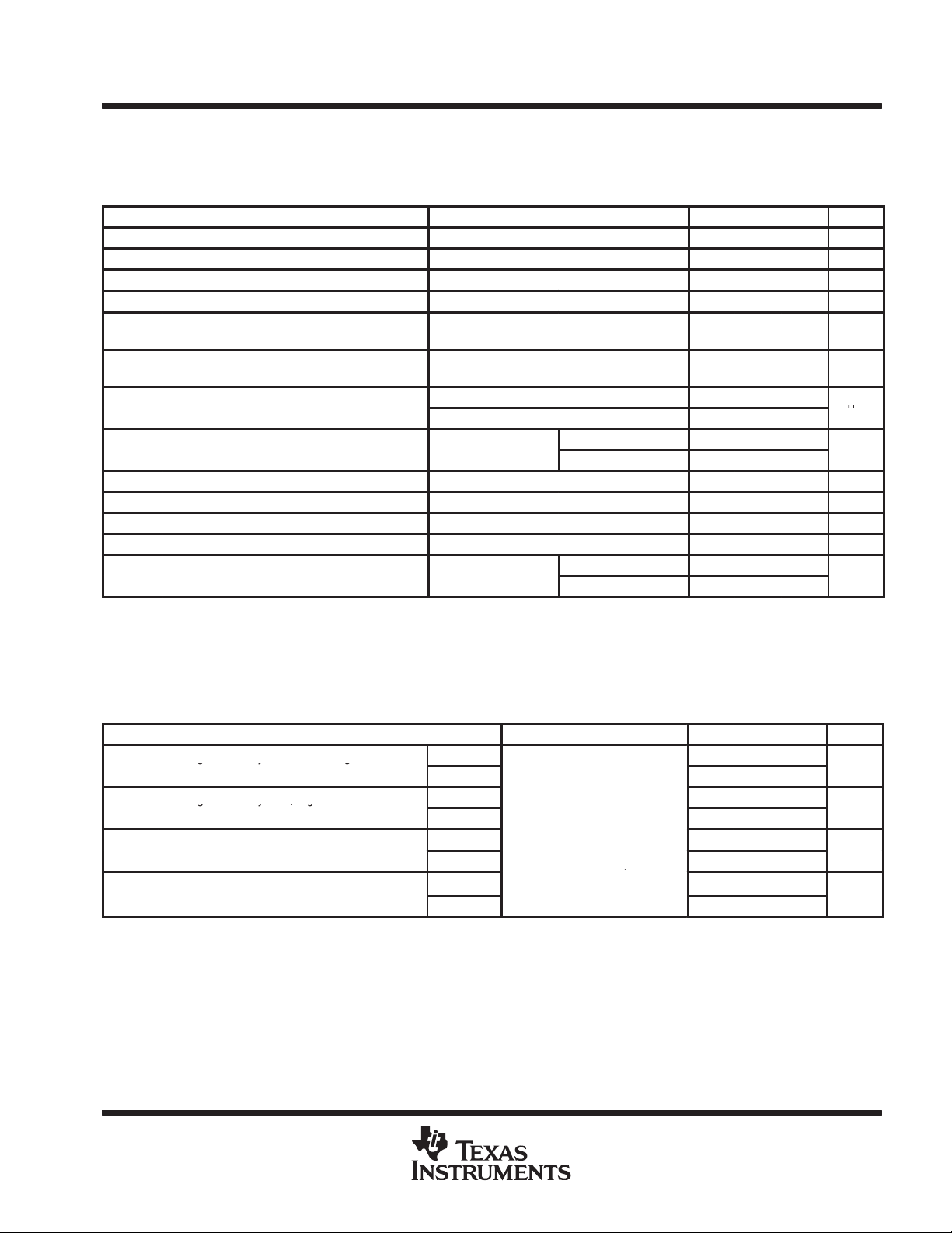
PACKAGE OPTION ADDENDUM
www.ti.com
10-May-2007
PACKAGING INFORMATION
Orderable Device Status
(1)
Package
Type
Package
Drawing
Pins Package
Qty
Eco Plan
SN75ALS170ADW ACTIVE SOIC DW 20 25 Green (RoHS &
no Sb/Br)
SN75ALS170ADWE4 ACTIVE SOIC DW 20 25 Green (RoHS &
no Sb/Br)
SN75ALS170ADWG4 ACTIVE SOIC DW 20 25 Green (RoHS &
no Sb/Br)
SN75ALS170ADWR ACTIVE SOIC DW 20 2000 Green (RoHS &
no Sb/Br)
SN75ALS170ADWRE4 ACTIVE SOIC DW 20 2000 Green (RoHS &
no Sb/Br)
SN75ALS170ADWRG4 ACTIVE SOIC DW 20 2000 Green (RoHS &
no Sb/Br)
SN75ALS170DW ACTIVE SOIC DW 20 25 Green (RoHS &
no Sb/Br)
SN75ALS170DWE4 ACTIVE SOIC DW 20 25 Green (RoHS &
no Sb/Br)
SN75ALS170DWG4 ACTIVE SOIC DW 20 25 Green (RoHS &
no Sb/Br)
SN75ALS170DWR ACTIVE SOIC DW 20 2000 Green (RoHS &
no Sb/Br)
SN75ALS170DWRE4 ACTIVE SOIC DW 20 2000 Green (RoHS &
no Sb/Br)
SN75ALS170DWRG4 ACTIVE SOIC DW 20 2000 Green (RoHS &
no Sb/Br)
SN75ALS170J OBSOLETE CDIP J 14 TBD Call TI Call TI
(1)
The marketing status values are defined as follows:
ACTIVE: Product device recommended for new designs.
LIFEBUY: TI has announced that the device will be discontinued, and a lifetime-buy period is in effect.
NRND: Not recommended for new designs. Device is in production to support existing customers, but TI does not recommend using this part in
a new design.
PREVIEW: Device has been announced but is not in production. Samples may or may not be available.
OBSOLETE: TI has discontinued the production of the device.
(2)
Lead/Ball Finish MSL Peak Temp
CU NIPDAU Level-1-260C-UNLIM
CU NIPDAU Level-1-260C-UNLIM
CU NIPDAU Level-1-260C-UNLIM
CU NIPDAU Level-1-260C-UNLIM
CU NIPDAU Level-1-260C-UNLIM
CU NIPDAU Level-1-260C-UNLIM
CU NIPDAU Level-1-260C-UNLIM
CU NIPDAU Level-1-260C-UNLIM
CU NIPDAU Level-1-260C-UNLIM
CU NIPDAU Level-1-260C-UNLIM
CU NIPDAU Level-1-260C-UNLIM
CU NIPDAU Level-1-260C-UNLIM
(3)
(2)
Eco Plan - The planned eco-friendly classification: Pb-Free (RoHS), Pb-Free (RoHS Exempt), or Green (RoHS & no Sb/Br) - please check
http://www.ti.com/productcontent for the latest availability information and additional product content details.
TBD: The Pb-Free/Green conversion plan has not been defined.
Pb-Free (RoHS): TI's terms "Lead-Free" or "Pb-Free" mean semiconductor products that are compatible with the current RoHS requirements
for all 6 substances, including the requirement that lead not exceed 0.1% by weight in homogeneous materials. Where designed to be soldered
at high temperatures, TI Pb-Free products are suitable for use in specified lead-free processes.
Pb-Free (RoHS Exempt): This component has a RoHS exemption for either 1) lead-based flip-chip solder bumps used between the die and
package, or 2) lead-based die adhesive used between the die and leadframe. The component is otherwise considered Pb-Free (RoHS
compatible) as defined above.
Green (RoHS & no Sb/Br): TI defines "Green" to mean Pb-Free (RoHS compatible), and free of Bromine (Br) and Antimony (Sb) based flame
retardants (Br or Sb do not exceed 0.1% by weight in homogeneous material)
(3)
MSL, Peak Temp. -- The Moisture Sensitivity Level rating according to the JEDEC industry standard classifications, and peak solder
temperature.
Important Information and Disclaimer:The information provided on this page represents TI's knowledge and belief as of the date that it is
provided. TI bases its knowledge and belief on information provided by third parties, and makes no representation or warranty as to the
accuracy of such information. Efforts are underway to better integrate information from third parties. TI has taken and continues to take
reasonable steps to provide representative and accurate information but may not have conducted destructive testing or chemical analysis on
incoming materials and chemicals. TI and TI suppliers consider certain information to be proprietary, and thus CAS numbers and other limited
Addendum-Page 1
Page 16

PACKAGE OPTION ADDENDUM
www.ti.com
information may not be available for release.
In no event shall TI's liability arising out of such information exceed the total purchase price of the TI part(s) at issue in this document sold by TI
to Customer on an annual basis.
10-May-2007
Addendum-Page 2
Page 17

PACKAGE MATERIALS INFORMATION
www.ti.com
TAPE AND REEL INFORMATION
11-Mar-2008
*All dimensions are nominal
Device Package
SN75ALS170ADWR SOIC DW 20 2000 330.0 24.4 10.8 13.1 2.65 12.0 24.0 Q1
SN75ALS170DWR SOIC DW 20 2000 330.0 24.4 10.8 13.1 2.65 12.0 24.0 Q1
Type
Package
Drawing
Pins SPQ Reel
Diameter
(mm)
Reel
Width
W1 (mm)
A0 (mm) B0 (mm) K0 (mm) P1
(mm)W(mm)
Pin1
Quadrant
Pack Materials-Page 1
Page 18

PACKAGE MATERIALS INFORMATION
www.ti.com
11-Mar-2008
*All dimensions are nominal
Device Package Type Package Drawing Pins SPQ Length (mm) Width (mm) Height (mm)
SN75ALS170ADWR SOIC DW 20 2000 346.0 346.0 41.0
SN75ALS170DWR SOIC DW 20 2000 346.0 346.0 41.0
Pack Materials-Page 2
Page 19

Page 20

Page 21

IMPORTANT NOTICE
Texas Instruments Incorporated and its subsidiaries (TI) reserve the right to make corrections, modifications, enhancements, improvements,
and other changes to its products and services at any time and to discontinue any product or service without notice. Customers should
obtain the latest relevant information before placing orders and should verify that such information is current and complete. All products are
sold subject to TI’s terms and conditions of sale supplied at the time of order acknowledgment.
TI warrants performance of its hardware products to the specifications applicable at the time of sale in accordance with TI’s standard
warranty. Testing and other quality control techniques are used to the extent TI deems necessary to support this warranty. Except where
mandated by government requirements, testing of all parameters of each product is not necessarily performed.
TI assumes no liability for applications assistance or customer product design. Customers are responsible for their products and
applications using TI components. To minimize the risks associated with customer products and applications, customers should provide
adequate design and operating safeguards.
TI does not warrant or represent that any license, either express or implied, is granted under any TI patent right, copyright, mask work right,
or other TI intellectual property right relating to any combination, machine, or process in which TI products or services are used. Information
published by TI regarding third-party products or services does not constitute a license from TI to use such products or services or a
warranty or endorsement thereof. Use of such information may require a license from a third party under the patents or other intellectual
property of the third party, or a license from TI under the patents or other intellectual property of TI.
Reproduction of TI information in TI data books or data sheets is permissible only if reproduction is without alteration and is accompanied
by all associated warranties, conditions, limitations, and notices. Reproduction of this information with alteration is an unfair and deceptive
business practice. TI is not responsible or liable for such altered documentation. Information of third parties may be subject to additional
restrictions.
Resale of TI products or services with statements different from or beyond the parameters stated by TI for that product or service voids all
express and any implied warranties for the associated TI product or service and is an unfair and deceptive business practice. TI is not
responsible or liable for any such statements.
TI products are not authorized for use in safety-critical applications (such as life support) where a failure of the TI product would reasonably
be expected to cause severe personal injury or death, unless officers of the parties have executed an agreement specifically governing
such use. Buyers represent that they have all necessary expertise in the safety and regulatory ramifications of their applications, and
acknowledge and agree that they are solely responsible for all legal, regulatory and safety-related requirements concerning their products
and any use of TI products in such safety-critical applications, notwithstanding any applications-related information or support that may be
provided by TI. Further, Buyers must fully indemnify TI and its representatives against any damages arising out of the use of TI products in
such safety-critical applications.
TI products are neither designed nor intended for use in military/aerospace applications or environments unless the TI products are
specifically designated by TI as military-grade or "enhanced plastic." Only products designated by TI as military-grade meet military
specifications. Buyers acknowledge and agree that any such use of TI products which TI has not designated as military-grade is solely at
the Buyer's risk, and that they are solely responsible for compliance with all legal and regulatory requirements in connection with such use.
TI products are neither designed nor intended for use in automotive applications or environments unless the specific TI products are
designated by TI as compliant with ISO/TS 16949 requirements. Buyers acknowledge and agree that, if they use any non-designated
products in automotive applications, TI will not be responsible for any failure to meet such requirements.
Following are URLs where you can obtain information on other Texas Instruments products and application solutions:
Products Applications
Amplifiers amplifier.ti.com Audio www.ti.com/audio
Data Converters dataconverter.ti.com Automotive www.ti.com/automotive
DSP dsp.ti.com Broadband www.ti.com/broadband
Clocks and Timers www.ti.com/clocks Digital Control www.ti.com/digitalcontrol
Interface interface.ti.com Medical www.ti.com/medical
Logic logic.ti.com Military www.ti.com/military
Power Mgmt power.ti.com Optical Networking www.ti.com/opticalnetwork
Microcontrollers microcontroller.ti.com Security www.ti.com/security
RFID www.ti-rfid.com Telephony www.ti.com/telephony
RF/IF and ZigBee® Solutions www.ti.com/lprf Video & Imaging www.ti.com/video
Mailing Address: Texas Instruments, Post Office Box 655303, Dallas, Texas 75265
Copyright © 2008, Texas Instruments Incorporated
Wireless www.ti.com/wireless
 Loading...