

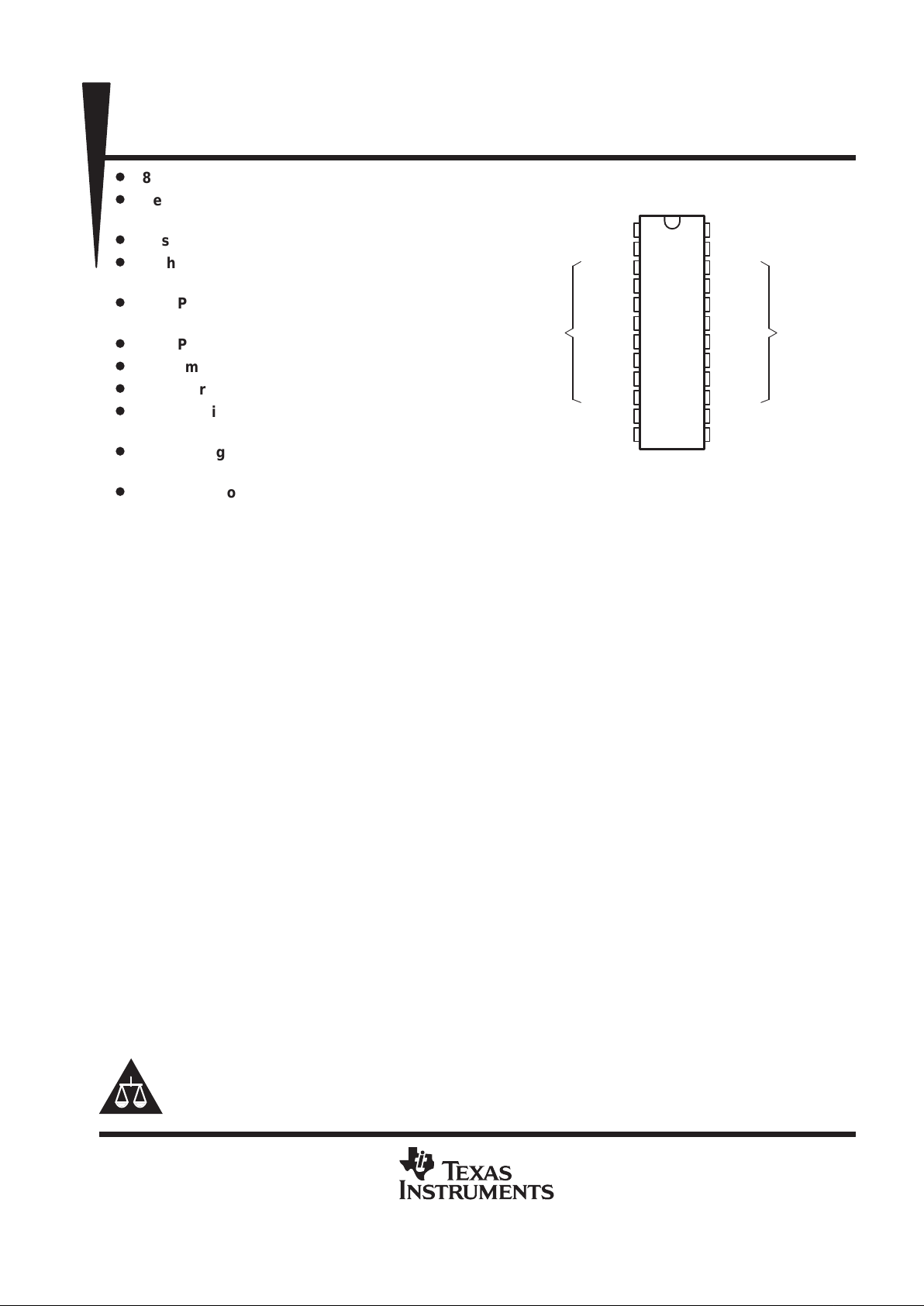
DW PACKAGE
(TOP VIEW)
GPIB
I/O Ports
Terminal
I/O Ports
1
2
3
4
5
6
7
8
9
10
11
12
24
23
22
21
20
19
18
17
16
15
14
13
SC
TE
REN
IFC
NDAC
NRFD
DAV
EOI
ATN
SRQ
NC
GND
V
CC
ATN+ EOI
REN
IFC
NDAC
NRFD
DAV
EOI
ATN
SRQ
NC
DC
NOT RECOMMENDED FOR NEW DESIGNS
NC – No internal connection
SN75ALS164
OCTAL GENERAL-PURPOSE INTERFACE BUS TRANSCEIVER
SLLS022C – JUNE 1986 – REVISED MA Y 1998
1
POST OFFICE BOX 655303 • DALLAS, TEXAS 75265
D
8-Channel Bidirectional Transceiver
D
Designed to Implement Control Bus
Interface
D
Designed for Multiple-Controller Systems
D
High-Speed Advanced Low-Power Schottky
Circuitry
D
Low-Power Dissipation...46 mW Max Per
Channel
D
Fast Propagation Times . . . 20 ns Max
D
High-Impedance pnp Inputs
D
Receiver Hysteresis...650 mV Typ
D
Bus-Terminating Resistors Provided on
Driver Outputs
D
No Loading of Bus When Device Is
Powered Down (V
CC
= 0)
D
Power-Up/Power-Down Protection
(Glitch Free)
description
The SN75ALS164 eight-channel general-purpose interface bus transceiver is a monolithic, high-speed,
advanced low-power Schottky device designed to meet the requirements of IEEE Standard 488-1978. Each
transceiver is designed to provide the bus-management and data-transfer signals between operating units of
a multiple-controller instrumentation system. When combined with the SN75ALS160 octal bus transceiver, the
SN75ALS164 provides the complete 16-wire interface for the IEEE 488 bus.
The SN75ALS164 features eight driver-receiver pairs connected in a front-to-back configuration to form
input/output (I/O) ports at both the bus and terminal sides. All outputs are disabled (at the high-impedance state)
during V
CC
power-up and power-down transitions for glitch-free operation. The direction of data flow through
these driver-receiver pairs is determined by the DC, TE, and SC enable signals. The SN75ALS164 is identical
to the SN75ALS162 with the addition of an OR gate to help simplify board layouts in several popular
applications. The ATN and EOI signals are ORed to provide the ATN + EOI output, which is a standard
totem-pole output.
The driver outputs (GPIB I/O ports) feature active bus-terminating resistor circuits designed to provide a high
impedance to the bus when supply voltage V
CC
is 0. The drivers are designed to handle loads up to 48 mA of
sink current. Each receiver features pnp transistor inputs for high input impedance and hysteresis of 400 mV
minimum for increased noise immunity . All receivers have 3-state outputs that present a high impedance to the
terminal when disabled.
The SN75ALS164 is characterized for operation from 0°C to 70°C.
Copyright 1998, Texas Instruments Incorporated
PRODUCTION DATA information is current as of publication date.
Products conform to specifications per the terms of Texas Instruments
standard warranty. Production processing does not necessarily include
testing of all parameters.
Please be aware that an important notice concerning availability, standard warranty, and use in critical applications of
Texas Instruments semiconductor products and disclaimers thereto appears at the end of this data sheet.
SN75ALS164
OCTAL GENERAL-PURPOSE INTERFACE BUS TRANSCEIVER
SLLS022C – JUNE 1986 – REVISED MA Y 1998
2
POST OFFICE BOX 655303 • DALLAS, TEXAS 75265
CHANNEL IDENTIFICATION TABLE
NAME
IDENTITY CLASS
DC
TE
SC
Direction-Control
Talk-Enable
System Control
Control
ATN
SRQ
REN
IFC
EOI
Attention
Service Request
Remote Enable
Interface Clear
End or Identity
Bus
Management
ATN+EOI ATN Logical or EOI Logic
DAV
NDAC
NRFD
Data Valid
No Data Accepted
Not Ready for Data
Data
Transfer
Function Tables
RECEIVE/TRANSMIT FUNCTION TABLE
CONTROLS
BUS-MANAGEMENT CHANNELS DATA-TRANSFER CHANNELS
SC DC TE ATN
†
ATN
†
SRQ REN IFC EOI DAV NDAC NRFD
(controlled by DC) (controlled by SC) (controlled by TE)
H H H
T
H H L
R
TRT
R
R
L L H
R
L L L
T
RTR
T
T
H L X R T R R T T
L H X T R T T R R
H T T
L R R
H = high level, L = low level, R = receive, T = transmit, X = irrelevant
Direction of data transmission is from the terminal side to the bus side, and the direction of data receiving is from the bus side to the terminal side.
Data transfer is noninverting in both directions.
†
ATN is a normal transceiver channel that functions additionally as an internal direction control or talk enable for EOI when the DC and TE inputs
are in the same state. When DC and TE are in opposite states, the ATN channel functions as an independent transceiver only.
ATN + EOI FUNCTION TABLE
INPUTS
OUTPUT
ATN EOI
ATN + EOI
H X H
X HH
LLL
SN75ALS164
OCTAL GENERAL-PURPOSE INTERFACE BUS TRANSCEIVER
SLLS022C – JUNE 1986 – REVISED MA Y 1998
3
POST OFFICE BOX 655303 • DALLAS, TEXAS 75265
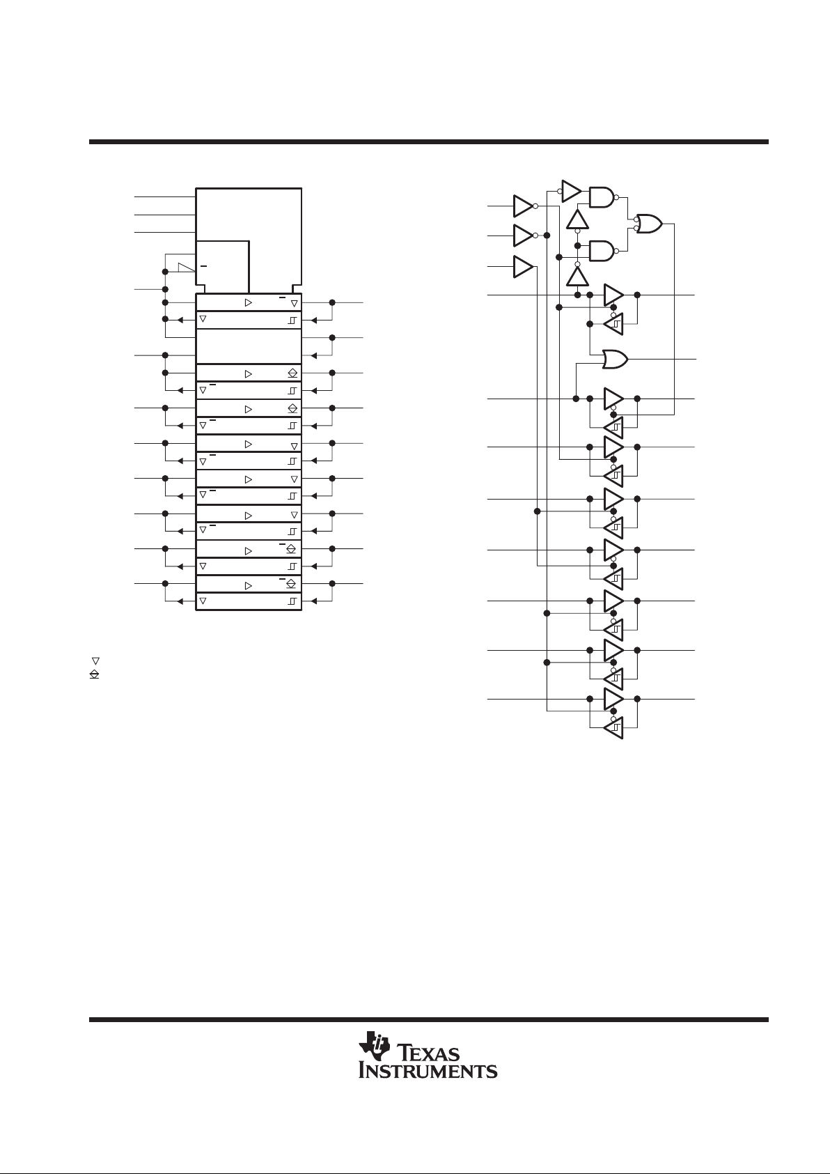
logic symbol
†
EN3
EN2/G5
3
2
2
3
DAV
NDAC
EOI
SRQ
REN
IFC
6
6
1
5
7
4
3
10
8
15
22
21
18
20
NDAC
DAV
IFC
REN
SRQ
ATN + EOI
23
17
EOI
1
1
1
1
1 1
11
ATN
9
EN6
4
5
ATN
16
SC
TE
≥ 1
2
2
3
1
1
†
This symbol is in accordance with ANSI/IEEE Std 91-1984 and
IEC Publication 617-12.
EN1/G4DC
1
2
13
≥ 1
2
NRFD
6
19
NRFD
1
2
3
Designates 3-state outputs
Designates passive-pullup outputs
logic diagram (positive logic)
13
DC
TE
2
ATN + EOI
23
9
16
ATN
ATN
EOI
EOI
17
8
SRQ
SRQ
15
10
3
22
REN
REN
4
21
IFC
IFC
DAV
DAV
18
7
5
20
NDAC
NDAC
SC
1
6
19
NRFD
NRFD
SN75ALS164
OCTAL GENERAL-PURPOSE INTERFACE BUS TRANSCEIVER
SLLS022C – JUNE 1986 – REVISED MA Y 1998
4
POST OFFICE BOX 655303 • DALLAS, TEXAS 75265
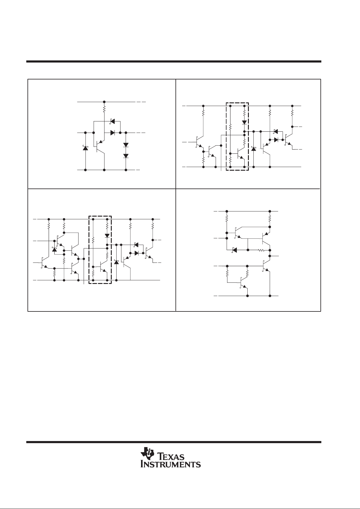
schematics of inputs and outputs
EQUIVALENT OF ALL
CONTROL INPUTS
TYPICAL OF SRQ, NDAC, AND NRFD
GPIB I/O PORT
Circuit inside dashed lines is on the driver outputs only.
TYPICAL OF ALL I/O PORTS
EXCEPT SRQ, NDAC, AND NRFD GPIB I/O PORTS
Receiver output Req = 110 Ω NOM
Driver output Req = 30 Ω NOM
GND
Input
V
CC
NOM
9 kΩ
10 kΩ
NOM
1.7 kΩ
NOM
NOM
4 kΩ
Input/Output Port
10 kΩ
NOM
1.7 kΩ
NOM
NOM
4 kΩ
R
eq
NOM
4 kΩ
Input/Output Port
ATN + EOI OUTPUT
GND
Output
V
CC
8 kΩ 200 kΩ
4.6 kΩ
2.5 kΩ1.3 kΩ
GND
V
CC
GND
V
CC
Circuit inside dashed lines is on the driver outputs only.
absolute maximum ratings over operating free-air temperature range (unless otherwise noted)
†
Supply voltage, V
CC
(see Note 1) 7 V. . . . . . . . . . . . . . . . . . . . . . . . . . . . . . . . . . . . . . . . . . . . . . . . . . . . . . . . . . . . .
Input voltage 5.5 V. . . . . . . . . . . . . . . . . . . . . . . . . . . . . . . . . . . . . . . . . . . . . . . . . . . . . . . . . . . . . . . . . . . . . . . . . . . . .
Low-level driver output current 100 mA. . . . . . . . . . . . . . . . . . . . . . . . . . . . . . . . . . . . . . . . . . . . . . . . . . . . . . . . . . . .
Package thermal impedance, θ
JA
(see Note 2) 81°C/W. . . . . . . . . . . . . . . . . . . . . . . . . . . . . . . . . . . . . . . . . . . . .
Storage temperature range, T
stg
–65°C to 150°C. . . . . . . . . . . . . . . . . . . . . . . . . . . . . . . . . . . . . . . . . . . . . . . . . .
Lead temperature 1,6 mm (1/16 inch) from the case for 10 seconds 260°C. . . . . . . . . . . . . . . . . . . . . . . . . . . .
†
Stresses beyond those listed under “absolute maximum ratings” may cause permanent damage to the device. These are stress ratings only, and
functional operation of the device at these or any other conditions beyond those indicated under “recommended operating conditions” is not
implied. Exposure to absolute-maximum-rated conditions for extended periods may affect device reliability.
NOTES: 1. All voltage values are with respect to network ground terminal.
2. The package thermal impedance is calculated in accordance with JESD 51.
 Loading...