SN75ALS163
OCTAL GENERAL-PURPOSE INTERFACE BUS TRANSCEIVER
SLLS021E – JUNE 1986 – REVISED MA Y 1998
1
POST OFFICE BOX 655303 • DALLAS, TEXAS 75265
D
8-Channel Bidirectional Transceiver
D
High-Speed Advanced Low-Power Schottky
Circuitry
D
Low Power Dissipation...46 mW Max per
Channel
D
Fast Propagation Times . . . 20 ns Max
D
High-Impedance pnp Inputs
D
Receiver Hysteresis...650 mV Typ
D
Open-Collector Driver Output Option
D
No Loading of Bus When Device Is
Powered Down (V
CC
= 0)
D
Power-Up/Power-Down Protection
(Glitch Free)
description
The SN75ALS163 octal general-purpose interface bus transceiver is a monolithic, high-speed, advanced
low-power Schottky device. It is designed for two-way data communications over single-ended transmission
lines. The transceiver features driver outputs that can be operated in either the open-collector or 3-state mode.
If talk enable (TE) is high, these outputs have the characteristics of open-collector outputs when pullup enable
(PE) is low and of 3-state outputs when PE is high. T aking TE low places the outputs in the high-impedance state.
The driver outputs are designed to handle loads of up to 48 mA of sink current. Each receiver features pnp
transistor inputs for high input impedance and 400 mV minimum of hysteresis for increased noise immunity.
Output glitches during power up and power down are eliminated by an internal circuit that disables both the bus
and receiver outputs. The outputs do not load the bus when V
CC
= 0.
The SN75ALS163 is characterized for operation from 0°C to 70°C.
Copyright 1998, Texas Instruments Incorporated
PRODUCTION DATA information is current as of publication date.
Products conform to specifications per the terms of Texas Instruments
standard warranty. Production processing does not necessarily include
testing of all parameters.
Please be aware that an important notice concerning availability, standard warranty, and use in critical applications of
Texas Instruments semiconductor products and disclaimers thereto appears at the end of this data sheet.
1
2
3
4
5
6
7
8
9
10
20
19
18
17
16
15
14
13
12
11
TE
B1
B2
B3
B4
B5
B6
B7
B8
GND
V
CC
D1
D2
D3
D4
D5
D6
D7
D8
PE
DW PACKAGE
(TOP VIEW)
GPIB
I/O
Ports
Terminal
I/O Ports
NOT RECOMMENDED FOR NEW DESIGNS

SN75ALS163
OCTAL GENERAL-PURPOSE INTERFACE BUS TRANSCEIVER
SLLS021E – JUNE 1986 – REVISED MA Y 1998
2
POST OFFICE BOX 655303 • DALLAS, TEXAS 75265
Function Tables
EACH DRIVER
INPUTS
OUTPUT
D TE PE
B
H H H H
L HX L
HXL Z
XLX Z
EACH RECEIVER
INPUTS
OUTPUT
B TE PE
D
L L X L
H LX H
XHX Z
H = high level, L = low level,
X = irrelevant, Z = high-impedance state
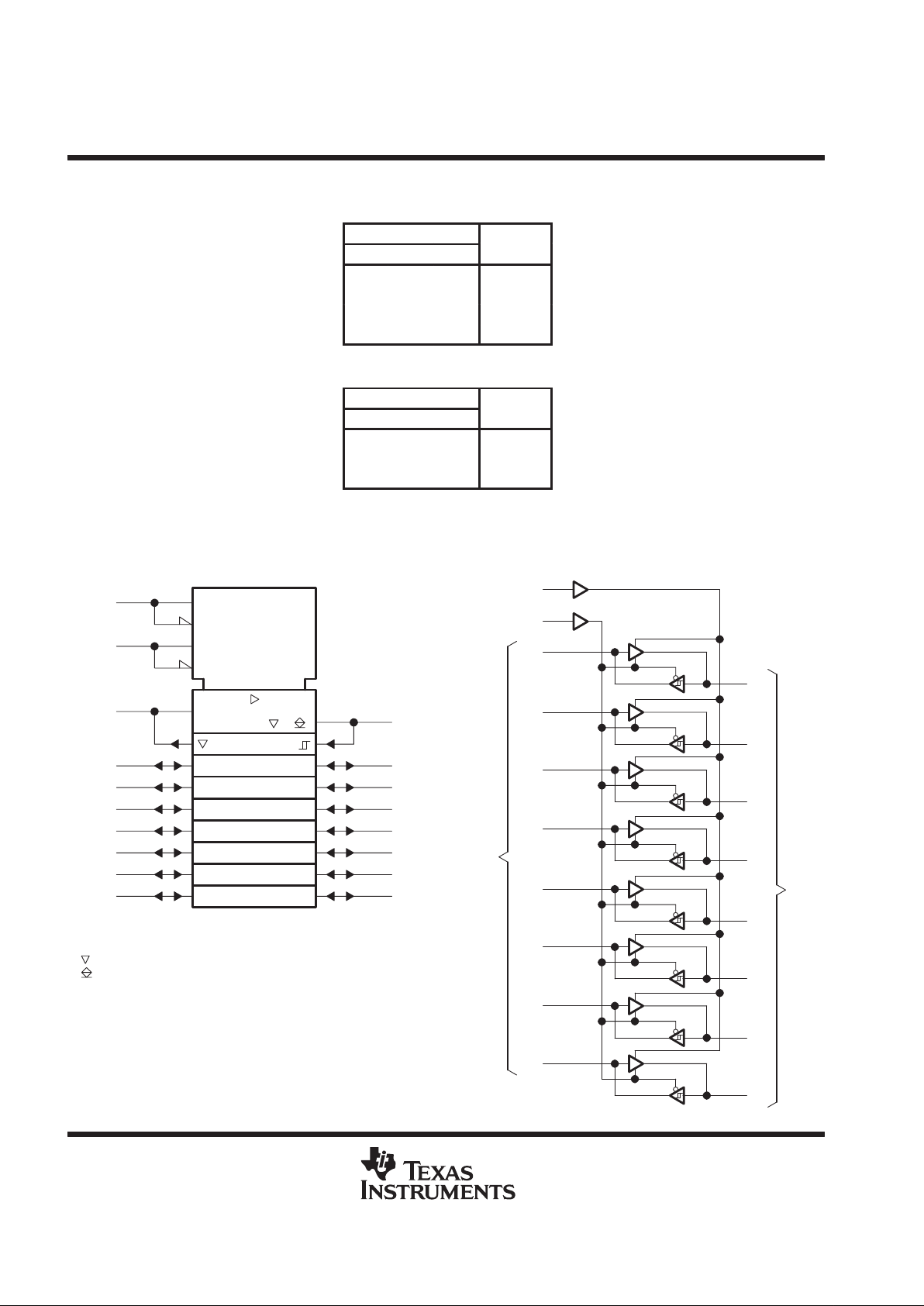
logic symbol
†
†
This symbol is in accordance with ANSI/IEEE Std 91-1984
and IEC Publication 617-12.
Designates 3-state outputs
Designates open-collector outputs
1
EN4 [RCV]
EN3 [XMT]
M2 [0C]
M1 [3S]
B8
B7
B6
B5
B4
B3
B2
B1
9
8
7
6
5
4
3
2
D8
D7
D6
D5
D4
D3
D2
D1
TE
PE
12
13
14
15
16
17
18
19
1
11
/23 (1 )
4
logic diagram (positive logic)
GPIB
I/O
Ports
PE
11
1
TE
Terminal
I/O
Ports
B1
2
19
D1
B2
3
18
D2
B3
4
17
D3
B4
5
16
D4
B5
6
15
D5
B6
7
14
D6
D7
13
8
B7
9
12
D8
B8

SN75ALS163
OCTAL GENERAL-PURPOSE INTERFACE BUS TRANSCEIVER
SLLS021E – JUNE 1986 – REVISED MA Y 1998
3
POST OFFICE BOX 655303 • DALLAS, TEXAS 75265
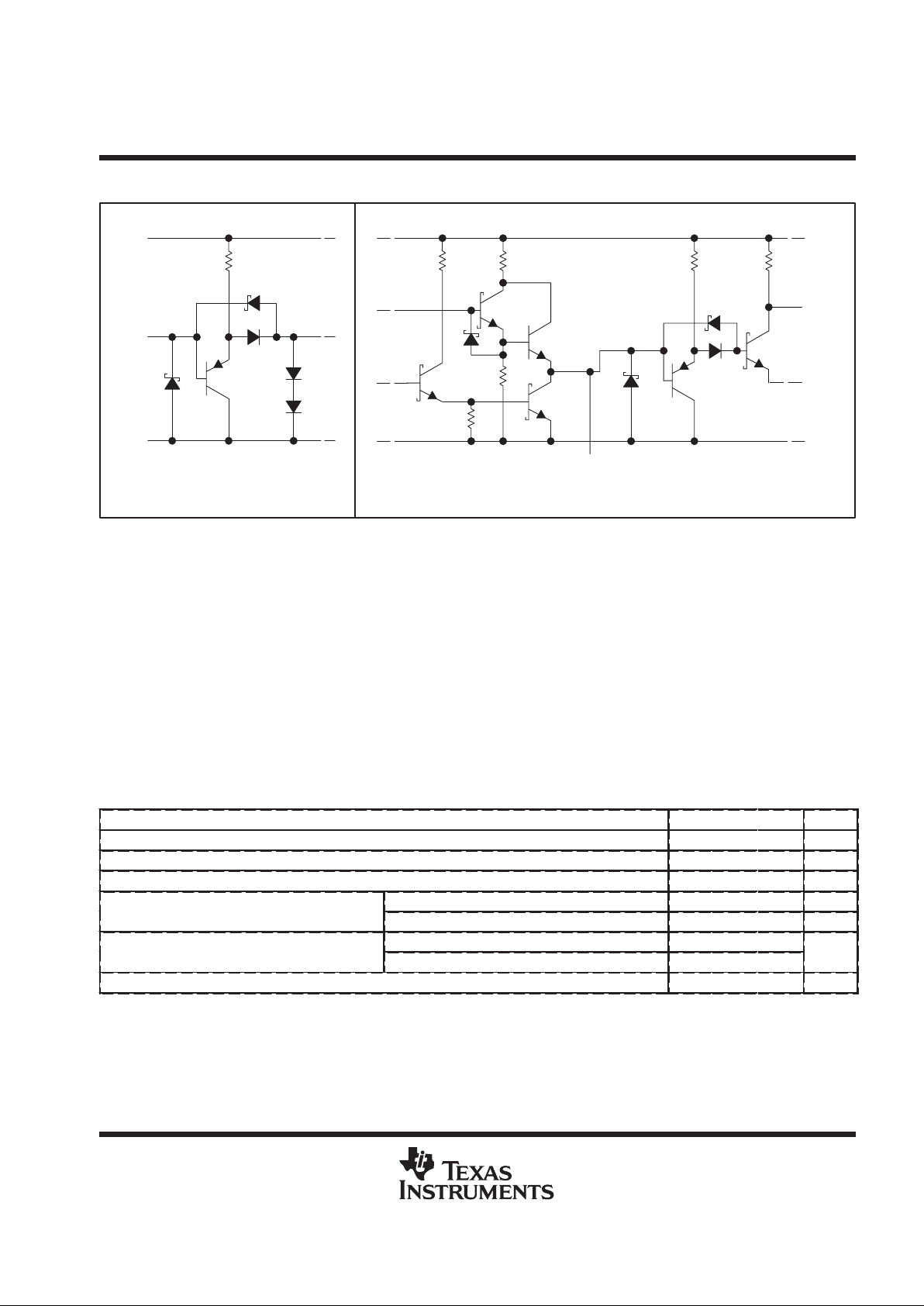
schematics of inputs and outputs
10 kΩ
NOM
EQUIVALENT OF ALL INPUT/OUTPUT PORTS
R
eq
NOM
4 kΩ
Input/Output Port
Receiver output Req = 110 Ω NOM
Driver output Req = 30 Ω NOM
GND
Input
V
CC
9 kΩ NOM
EQUIVALENT OF ALL CONTROL INPUTS
V
CC
GND
absolute maximum ratings over operating free-air temperature range (unless otherwise noted)
†
Supply voltage, V
CC
(see Note 1) 7 V. . . . . . . . . . . . . . . . . . . . . . . . . . . . . . . . . . . . . . . . . . . . . . . . . . . . . . . . . . . . .
Input voltage, V
I
5.5 V. . . . . . . . . . . . . . . . . . . . . . . . . . . . . . . . . . . . . . . . . . . . . . . . . . . . . . . . . . . . . . . . . . . . . . . . . .
Low-level driver output current 100 mA. . . . . . . . . . . . . . . . . . . . . . . . . . . . . . . . . . . . . . . . . . . . . . . . . . . . . . . . . . . .
Package thermal impedance, θ
JA
(see Note 2) 97°C/W. . . . . . . . . . . . . . . . . . . . . . . . . . . . . . . . . . . . . . . . . . . . .
Storage temperature range, T
stg
–65°C to 150°C. . . . . . . . . . . . . . . . . . . . . . . . . . . . . . . . . . . . . . . . . . . . . . . . . .
Lead temperature 1,6 mm (1/16 inch) from the case for 10 seconds 260°C. . . . . . . . . . . . . . . . . . . . . . . . . . . .
†
Stresses beyond those listed under “absolute maximum ratings” may cause permanent damage to the device. These are stress ratings only, and
functional operation of the device at these or any other conditions beyond those indicated under “recommended operating conditions” is not
implied. Exposure to absolute-maximum-rated conditions for extended periods may affect device reliability.
NOTES: 1. All voltage values are with respect to network ground terminal.
2. The package thermal impedance is calculated in accordance with JESD 51.
recommended operating conditions
MIN NOM MAX UNIT
Supply voltage, V
CC
4.75 5 5.25 V
High-level input voltage, V
IH
2 V
Low-level input voltage, V
IL
0.8 V
p
Bus ports with pullups active – 5.2 mA
High-level output current, I
OH
Terminal ports – 800 µA
p
Bus ports 48
Low-level output current, I
OL
Terminal ports 16
mA
Operating free-air temperature, T
A
0 70 °C
 Loading...