

SN75ALS085
LAN ACCESS UNIT INTERFACE DUAL DRIVER/RECEIVER
SLLS054B – APRIL 1989 – REVISED MA Y 1995
1
POST OFFICE BOX 655303 • DALLAS, TEXAS 75265
D
Meets or Exceeds the Requirements of IOS
8802.3:1989 and ANSI/IEEE Std 802.3-1988
D
Interdevice Loop-Back Paths for System
Testing
D
Squelch Function Implemented on the
Receiver Inputs
D
Drivers Will Drive a Balanced 78-Ω Load
D
Transformer Coupling Not Required in
System
D
Power-Up/Power-Down Protection (Glitch
Free)
D
Isolated Ground Pins for Reduced Noise
Coupling
D
Fault-Condition Protection Built into the
Device
D
Driver Inputs Are Level-Shifted ECL
Compatible
description
The SN75ALS085 is a monolithic, high-speed, advanced low-power Schottky, dual-channel driver/receiver
device designed for use in the AUI of ANSI/IEEE Std 802.3-1988. The two drivers on the device drive a 78-Ω
balanced, terminated twisted-pair transmission line up to a maximum length of 50 meters. In the off (idle) state,
the drivers maintain minimal differential output voltage on the twisted-pair line and, at the same time, remain
within the required output common-mode range.
With the driver enable (TXEN) high, upon receiving the first falling edge into the driver input, the differential
outputs will rise to full-amplitude output levels within 25 ns. The output amplitude is maintained for the remainder
of the packet. After the last positive packet edge is transmitted into the driver, the driver will maintain a minimum
of 70% full differential output for a minimum of 200 ns, then decay to a minimum level for the reset (idle) condition
within 8 µs. Disabling the driver by taking the driver enable low will also force the output into the idle condition
after the normal 8-µs timeout. While operating, the drivers are able to withstand a set of fault conditions and not
suffer damage due to the faults being applied. The drivers power up in the idle state to ensure that no activity
is placed on the twisted-pair cable that could be interpreted as network traffic.
The line receiver squelch function interfaces to a differential twisted-pair line terminated external to the device.
The receiver squelch circuit allows differential receive signals to pass through as long as the input amplitude
and pulse duration are greater than the minimum squelch threshold. This ensures a good signal-to-noise ratio
while the data path is active and prevents system noise from causing false data transitions during line shutdown
and line-idle conditions. The RXO outputs default to a high level and the RXEN outputs default to a low level
while the squelch function is blocking the data path through the receiver (idle). The line receiver squelch will
become active within 50 ns when the input squelch threshold is exceeded. RXEN will be driven high when the
squelch circuit is allowing data to pass through the receiver. The receiver squelch circuit can also withstand a
set of fault conditions while operating without causing permanent damage to the device.
Copyright 1995, Texas Instruments Incorporated
PRODUCTION DATA information is current as of publication date.
Products conform to specifications per the terms of Texas Instruments
standard warranty. Production processing does not necessarily include
testing of all parameters.
Please be aware that an important notice concerning availability, standard warranty, and use in critical applications of
Texas Instruments semiconductor products and disclaimers thereto appears at the end of this data sheet.
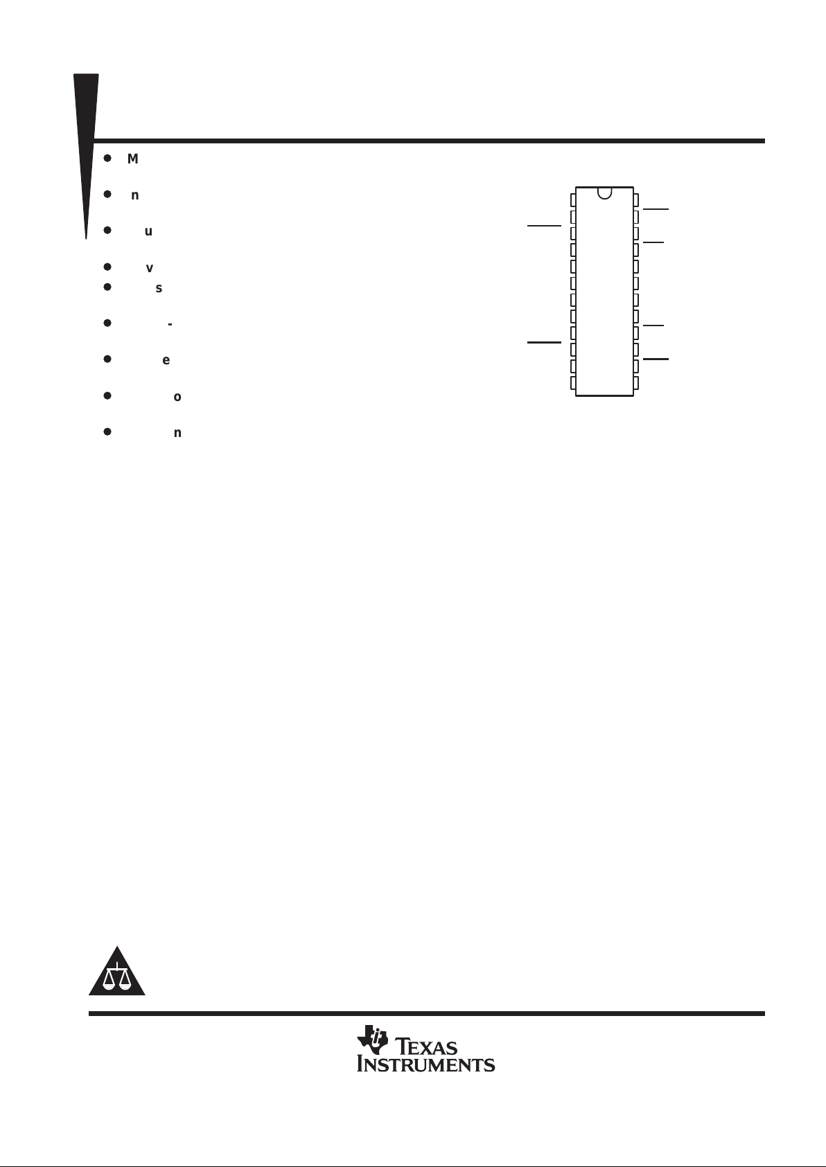
DW OR NT PACKAGE
(TOP VIEW)
1
2
3
4
5
6
7
8
9
10
11
12
24
23
22
21
20
19
18
17
16
15
14
13
TXI1
TXEN1
LOOP
1
GND
RXEN1
RXO1
RXO2
RXEN2
GND
LOOP
2
TXEN2
TXI2
TXO1
TXO
1
V
CC
RXI1
RXI1
GND
GND
RXI2
RXI
2
V
CC
TXO2
TXO2
SN75ALS085
LAN ACCESS UNIT INTERFACE DUAL DRIVER/RECEIVER
SLLS054B – APRIL 1989 – REVISED MA Y 1995
2
POST OFFICE BOX 655303 • DALLAS, TEXAS 75265
description (continued)
The purpose of the loop functions is to provide a means by which system data path verification can be done
to isolate faulty interfaces and assist in network diagnosis. The LOOP pins are TTL compatible and must be
held high for normal operation. When LOOP1
is taken low, the output of driver 1 (TXO1) immediately goes into
the idle state. Also, the input to receiver 1 is ignored and a path from TXI1 to RXO1 is established. When LOOP1
is taken back high, driver 1 and receiver 1 revert back to their normal operation. When LOOP2 is taken low , a
similar data path is established between TXI1 and RXO2. TXEN1 must be high for the loop functions to operate
and TXEN1 can be used to gate the loop function if desired. During loop operation, the respective receiver
enable output (RXEN) will reflect the status of TXEN1.
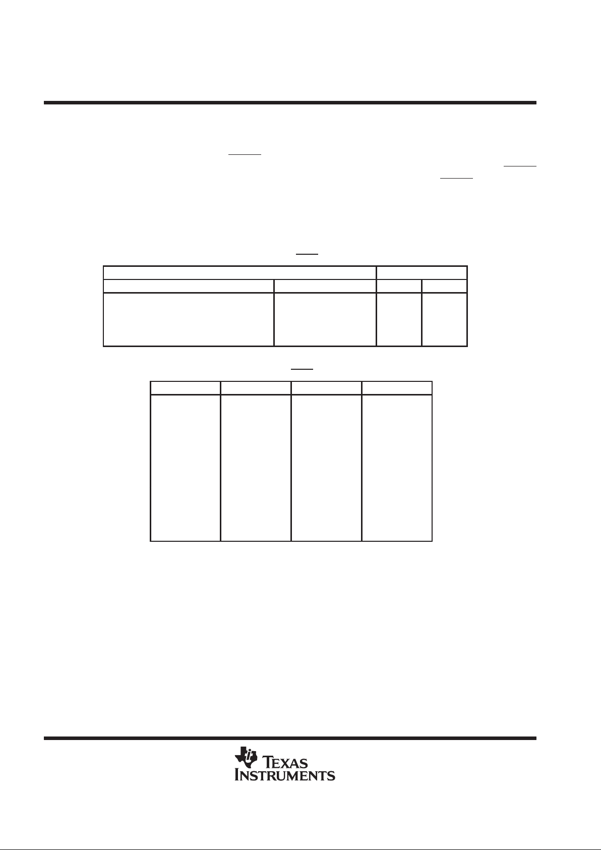
Function Tables
RECEIVER – LOOP = H
OUTPUTS
RXI PREVIOUS RXEN RXEN RXO
VID = 1315 mV to –175 mV , tw < 25 ns L L H
VID = –275 mV to –1315 mV , tw > 50 ns X H L
VID = 318 mV to 1315 mV , tw < 142 ns H H H
VID = 318 mV to 1315 mV , tw > 187 ns X L H
H = high level, L = low level, X = don’t care
DRIVER – LOOP
= H
TXI
TXEN PREVIOUS TXO OUTPUT TXO
L L Idle Idle
H L Idle Idle
↓ H Idle L
L H Active L
H < 260 µs H Active H
H > 8 µs H Active Idle
L L > 8 µs Active Idle
H < 260 ns L > 8 µs Active Idle
H < 260 ns L < 260 ns Active H
H > 8 µs L < 260 ns Active Idle
L L < 260 ns Active L
H = VI ≥ VT max, L = VI ≤ VT min
SN75ALS085
LAN ACCESS UNIT INTERFACE DUAL DRIVER/RECEIVER
SLLS054B – APRIL 1989 – REVISED MA Y 1995
3
POST OFFICE BOX 655303 • DALLAS, TEXAS 75265
Function Tables (continued)
LOOP
INPUTS
OUTPUTS
LOOP1 LOOP2 TXI1 TXEN1 RXI1 RXI2 RXO1 RXO2 RXEN1 RXEN2 TXO1
L L L H X X L L H H Idle
L LHHXXHH H H Idle
L LXLXXHH L L Idle
L H L H X Normal L Normal H Normal Idle
L H H H X Normal H Normal H Normal Idle
L H X L X Normal H Normal L Normal Idle
H L L H Normal X Normal L Normal H Idle
H L H H Normal X Normal H Normal H Idle
H L X L Normal X Normal H Normal L Idle
H H Normal Normal Normal Normal Normal Normal Normal Normal Normal
H = high level, L = low level, X = don’t care
SN75ALS085
LAN ACCESS UNIT INTERFACE DUAL DRIVER/RECEIVER
SLLS054B – APRIL 1989 – REVISED MA Y 1995
4
POST OFFICE BOX 655303 • DALLAS, TEXAS 75265
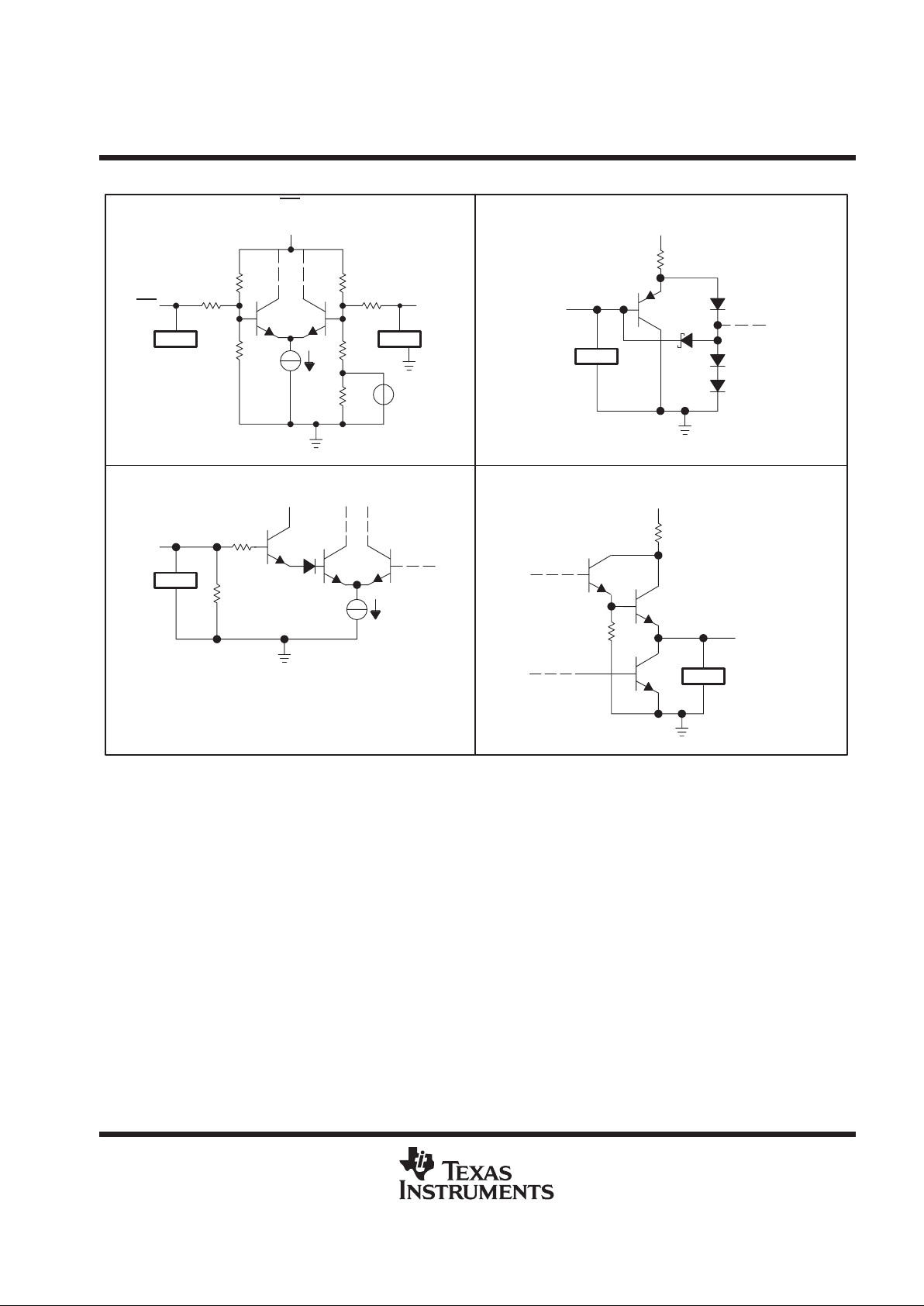
logic diagram (positive logic)
150 ns
5
RXEN1
RXO1
6
1
1
X1
TXO1
TXO1
23
24
1
1
X1
250 ns
4 µS
ECL/TTL
Noise
Filter
+–
225 mV
RX11
20
RX11
21
LOOP1
3
TXI1
1
TXEN1
2
LOOP2
10
7
RXO2
150 ns
RXEN2
8
14
13
TXO
2
TXO2
4 µS
250 ns
Noise
Filter
ECL/TTL
225 mV
–+
RXI2
17
16
12
TXI2
11
TXEN2
RXI2
SN75ALS085
LAN ACCESS UNIT INTERFACE DUAL DRIVER/RECEIVER
SLLS054B – APRIL 1989 – REVISED MA Y 1995
5
POST OFFICE BOX 655303 • DALLAS, TEXAS 75265
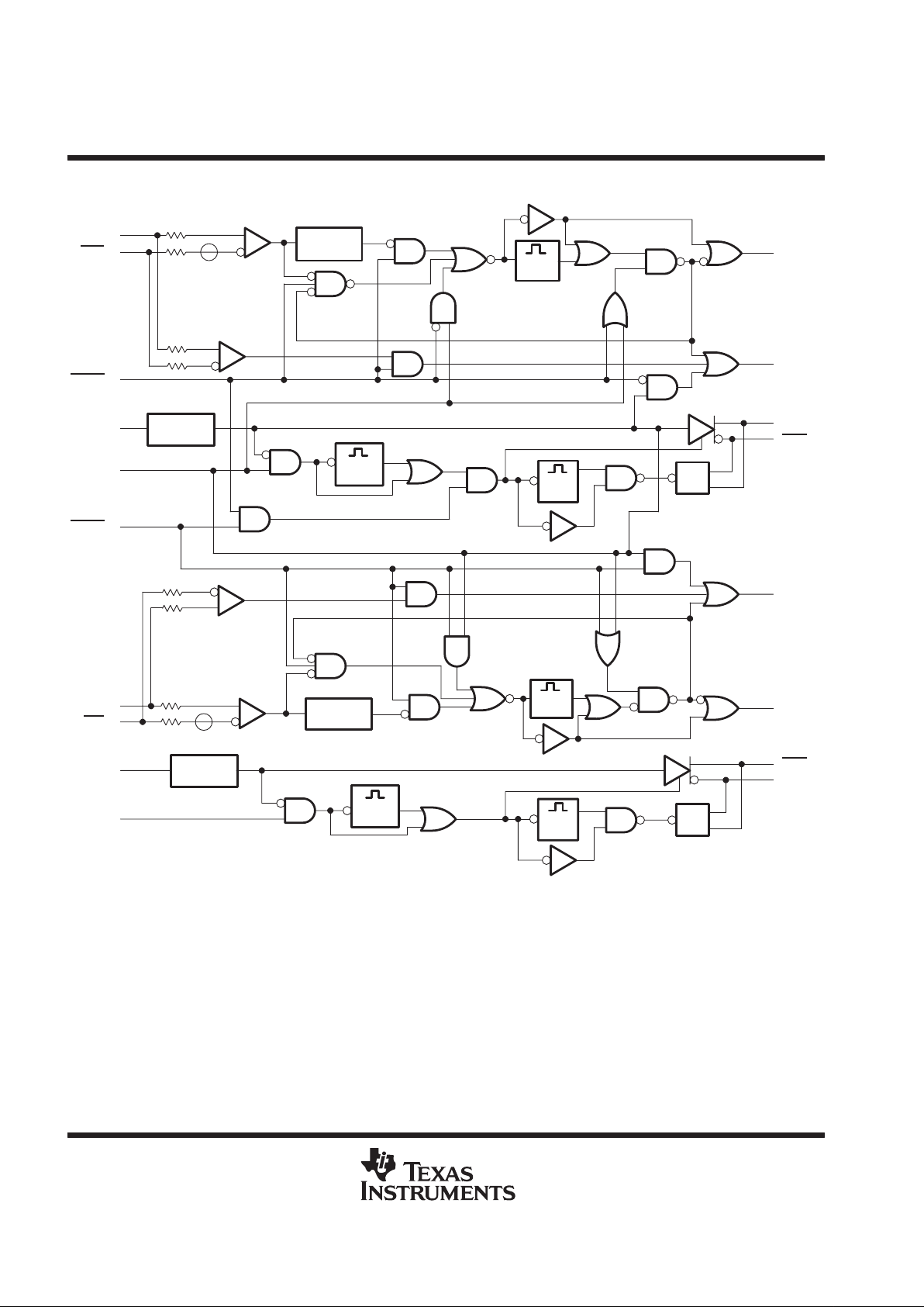
schematics of inputs and outputs
50 Ω
5 kΩ
RXO
and
RXEN
ESD
V
CC
20 kΩ
LOOP
and
TXEN
V
CC
ESD
RXI
ESD
–
+
1 kΩ
3 kΩ
4 kΩ
4 kΩ
4 kΩ4 kΩ
4 kΩ
RXI
ESD
V
CC
TXI
V
CC
200 Ω
50 kΩ
ESD
RXI AND RXI INPUTS LOOP AND TXEN INPUTS
RXO AND RXEN OUTPUTSTXI INPUTS
SN75ALS085
LAN ACCESS UNIT INTERFACE DUAL DRIVER/RECEIVER
SLLS054B – APRIL 1989 – REVISED MA Y 1995
6
POST OFFICE BOX 655303 • DALLAS, TEXAS 75265
absolute maximum ratings over operating free-air temperature range (unless otherwise noted)
Supply voltage, VCC (see Note 1) 6 V. . . . . . . . . . . . . . . . . . . . . . . . . . . . . . . . . . . . . . . . . . . . . . . . . . . . . . . . . . . . .
TXI and LOOP
input voltage, VI 5.5 V. . . . . . . . . . . . . . . . . . . . . . . . . . . . . . . . . . . . . . . . . . . . . . . . . . . . . . . . . . . . .
TXO and TXO
output voltage, VO 16 V. . . . . . . . . . . . . . . . . . . . . . . . . . . . . . . . . . . . . . . . . . . . . . . . . . . . . . . . . . . .
RXI and RXI
input voltage, VI 16 V. . . . . . . . . . . . . . . . . . . . . . . . . . . . . . . . . . . . . . . . . . . . . . . . . . . . . . . . . . . . . . . .
RXO and RXEN output voltage, V
O
5.5 V. . . . . . . . . . . . . . . . . . . . . . . . . . . . . . . . . . . . . . . . . . . . . . . . . . . . . . . . .
Continuous total power dissipation See Dissipation Rating Table. . . . . . . . . . . . . . . . . . . . . . . . . . . . . . . . . . . . .
Operating free-air temperature range, T
A
0°C to 70°C. . . . . . . . . . . . . . . . . . . . . . . . . . . . . . . . . . . . . . . . . . . . . .
Storage temperature range, T
stg
– 65 °C to 150 °C. . . . . . . . . . . . . . . . . . . . . . . . . . . . . . . . . . . . . . . . . . . . . . . . .
Lead temperature 1,6 mm (1/16 inch) from case for 10 seconds 260°C. . . . . . . . . . . . . . . . . . . . . . . . . . . . . . .
NOTE 1: Voltage values are with respect to network ground terminal.
DISSIPATION RATING TABLE
PACKAGE
TA ≤ 25°C
POWER RATING
DERATING FACTOR
ABOVE TA = 25°C
TA = 70°C
POWER RATING
DW 1350 mW 10.8 mW/°C 864 mW
NT 1250 mW 10.0 mW/°C 800 mW
recommended operating conditions
MIN NOM MAX UNIT
Supply voltage, V
CC
4.75 5 5.25 V
Common-mode voltage at RXI inputs, V
IC
1 4.2 V
Differential voltage between RXI inputs, V
ID
±318 ±1315 mV
High-level input voltage, LOOP and TXEN, V
IH
2 V
Low-level input voltage, LOOP and TXEN, V
IL
0.8 V
High-level output current, RXO and RXEN, I
OH
– 0.4 mA
Low-level output voltage, RXO and RXEN, I
OL
16 mA
Setup time, driver mode, TXEN high before TXI↓, t
su1
(see Figure 7) 10 ns
Setup time, loop mode, LOOP low before TXEN↑, t
su2
(see Figure 9) 15 ns
Setup time, loop mode, TXEN high before TXI↓, t
su3
(see Figure 9) 10 ns
Hold time, loop mode, TXEN high after TXI↑, th1 (see Figure 8) 10 ns
Hold time, loop mode, LOOP low after TXEN↓, th2 (see Figure 8) 15 ns
Operating free-air temperature, T
A
0 70 °C

SN75ALS085
LAN ACCESS UNIT INTERFACE DUAL DRIVER/RECEIVER
SLLS054B – APRIL 1989 – REVISED MA Y 1995
7
POST OFFICE BOX 655303 • DALLAS, TEXAS 75265
electrical characteristics over recommended ranges of supply voltage and operating free-air
temperature (unless otherwise noted)
PARAMETER TEST CONDITIONS MIN MAX UNIT
V
IK
Clamp voltage at all inputs II = –18 mA –1.5 V
VCC = 4.75 V 3.202 3.752
TA = 0°C
VCC = 5 V 3.389 3.998
V
VCC = 5.25 V 3.577 4.244
VCC = 4.75 V 3.213 3.797
V
(TO)
Driver input (TXI) threshold voltage TA = 25°C
VCC = 5 V 3.400 4.043
V
()
VCC = 5.25 V 3.588 4.289
VCC = 4.75 V 3.239 3.849
TA = 70°C
VCC = 5 V 3.426 4.095
V
VCC = 5.25 V 3.614 4.341
Receiver differential input threshold voltage –275 mV
Idle
TXEN at 0.8 V , LOOP1 at 2 V ,
LOOP
2 at 2 V, See Figure 1
1 4.2
V
OC
Driver output (TXO) common-mode voltage
Active
TXEN at 2 V, LOOP1 at 2 V,
LOOP
2 at 2 V , TXI at 3.2 V,
See Figure 1
1 4.2
V
Active
TXEN at 2 V, LOOP1 at 2 V,
LOOP
2 at 2 V , TXI at 4.4 V,
See Figure 1
1 4.2
Idle
TXEN at 0.8 V , LOOP1 at 2 V ,
LOOP
2 at 2 V, See Figure 1
±40
V
OD
Driver output (TXO) differential voltage
Active
TXEN at 2 V, LOOP1 at 2 V,
LOOP
2 at 2 V , TXI at 3.2 V,
See Figure 1
– 600 1315
mV
Active
TXEN at 2 V, LOOP1 at 2 V,
LOOP
2 at 2 V , TXI at 4.4 V,
See Figure 1
600 1315
V
OH
High-level output voltage RXO, RXEN IOH = –0.4 mA 2.4 V
V
OL
Low-level output voltage RXO, RXEN IOL = 16 mA 0.5 V
TXEN, LOOP VI = 2 V 20
I
IH
High-level input current
TXI
VI = 4.5 V 400
µA
RXI, RXI VID = –0.5 V, VIC = 1 V to 4.2 V 1000
TXEN, LOOP VI = 0.8 V –200
p
VI = 3.1 V 100
IILLow-level input current
TXI
VI = 0.3 V 4 10
mA
RXI, RXI VID = 0.5 V, VIC = 1 V to 4.2 V 1000
I
OD
Driver differential output current Idle
TXEN at 0.8 V , LOOP1 at 2 V ,
LOOP
2 at 2 V, See Figure 2
±4 mA
I
OS
Short-circuit output current
†
RXO, RXEN
VO at 0 V, RXI at 3 V,
RXI at 2 V
–40 – 150 mA
I
CC
Supply current
LOOP2 at 2 V, TXEN at 2 V,
TXI at 4.5 V , Outputs open
225 mA
†
Not more than one output should be shorted at a time, and the duration of the test should not exceed 1 second.

SN75ALS085
LAN ACCESS UNIT INTERFACE DUAL DRIVER/RECEIVER
SLLS054B – APRIL 1989 – REVISED MA Y 1995
8
POST OFFICE BOX 655303 • DALLAS, TEXAS 75265
electrical characteristics over recommended ranges of supply voltage and operating free-air
temperature (unless otherwise noted) (continued)
PARAMETER TEST CONDITIONS
†
MIN MAX UNIT
TXO shorted to TXO, Current measured in short 150
TXO at 0 V, TXO is open, Current measured at TXO 150
TXO is open, TXO at 0, Current measured at TXO 150
Driver fault condition current
TXO at 0 V, TXO at 0 V, Current measured at TXO and TXO 150
mA
TXO at 16 V, TXO is open, Current measured at TXO 150
TXO is open, TXO at 16 V, Current measured at TXO 150
TXO at 16 V, TXO at 16 V, Current measured at TXO and TXO 150
RXI shorted to RXI, Current measured in short 10
RXI at 0 V, RXI is open, Current measured at RXI 3
RXI is open, RXI at 0 V, Current measured at RXI 3
Receiver fault condition current
RXI at 0 V, RXI at 0 V, Current measured at RXI and RXI 3
mA
RXI at 16 V, RXI at open, Current measured at RXI 10
RXI at open, RXI at 16 V, Current measured at RXI 10
RXI at 16 V, RXI at 16 V, Current measured at RXI and RXI 10
†
Fault conditions should be measured on only one channel at a time.

SN75ALS085
LAN ACCESS UNIT INTERFACE DUAL DRIVER/RECEIVER
SLLS054B – APRIL 1989 – REVISED MA Y 1995
9
POST OFFICE BOX 655303 • DALLAS, TEXAS 75265
switching characteristics over recommended ranges of supply voltage and operating free-air
temperature (unless otherwise noted)
driver
PARAMETER
FROM
(INPUT)TO(OUTPUT)
TEST CONDITIONS MIN MAX UNIT
t
PLH
Propagation delay time,
low-to-high level output
TXI TXO, TXO TXEN at 2 V, See Figure 3 15 ns
t
PHL
Propagation delay time,
high-to-low level output
TXI TXO, TXO TXEN at 2 V, See Figure 3 15 ns
t
PIL
Propagation delay time,
idle-to-low level output
TXI TXO, TXO TXEN at 2 V, See Figure 4 25 ns
t
PIL
Propagation delay time,
idle-to-low level output
TXEN TXO, TXO TXI at 3.2 V, See Figure 5 25 ns
t
w
Output pulse duration from lowto-high level to 70% output level
TXO, TXO TXEN at 2 V, See Figure 6 260 8000 ns
V
OD(U)
Driver output differential
undershoot voltage
TXI TXO, TXO TXEN at 2 V, See Figure 6 –100 mV
t
sk
Driver caused signal skew
t
PLH
– t
PHL
TXI TXO, TXO TXEN at 2 V, See Figure 3 ±3 ns
t
r
Rise time, TXO, TXO TXEN at 2 V, See Figure 3 1 5 ns
t
f
Fall time, TXO, TXO TXEN at 2 V, See Figure 3 1 5 ns
receiver
PARAMETER
FROM
(INPUT)TO(OUTPUT)
TEST CONDITIONS MIN MAX UNIT
t
PLH
Propagation delay time,
low-to-high level output
RXI, RXI RXO VIC = 1 V to 4.2 V, See Figure 10 15 ns
t
PHL
Propagation delay time,
high-to-low level output
RXI, RXI RXO VIC = 1 V to 4.2 V, See Figure 10 15 ns
t
PLH
Start-up delay time,
low-to-high level output
RXI, RXI RXEN
VIC = 1 V to 4.2 V, VID = –500 mV,
See Figure 12
55 ns
t
PHL
Shutdown delay time,
high-to-low level output
RXI, RXI RXEN
VIC = 1 V to 4.2 V, VID = 500 mV ,
See Figure 12
142 181 ns
t
sk
Receiver caused signal
skew (t
PLH
– t
PHL
)
RXI, RXI RXO
VIC = 1 V to 4.2 V, VID = 500 mV ,
See Figure 10
±3 ns
t
w
Pulse duration at RXI and RXI
(to not activate squelch)
VIC = 1 V to 4.2 V, VID = –175 mV,
See Figure 11
25 ns
t
w
Pulse duration at RXI and RXI
(to activate squelch)
VIC = 1 V to 4.2 V, VID = –275 mV,
See Figure 11
50 ns
t
r1
Rise time, RXO
VIC = 1 V to 4.2 V, VID = ±500 mV ,
See Figure 10
1 8 ns
t
r2
Rise time, RXEN
VIC = 1 V to 4.2 V, VID = ±500 mV ,
See Figure 12
1 8 ns
t
f1
Fall time, RXO
VIC = 1 V to 4.2 V, VID = ±500 mV ,
See Figure 10
1 8 ns
t
f2
Fall time, RXEN
VIC = 2.5 V, VID = ±500 V ,
See Figure 12
1 8 ns
t
v
RXO valid after RXEN high See Figure 10 –10 15 ns

SN75ALS085
LAN ACCESS UNIT INTERFACE DUAL DRIVER/RECEIVER
SLLS054B – APRIL 1989 – REVISED MA Y 1995
10
POST OFFICE BOX 655303 • DALLAS, TEXAS 75265
switching characteristics over recommended ranges of supply voltage and operating free-air
temperature
loop
PARAMETER
FROM
(INPUT)
TO
(OUTPUT)
TEST CONDITIONS MIN MAX UNIT
t
PLH
Propagation delay time,
low-to-high level output
TXI RXO
LOOP at 0.8 V, TXEN at 2 V,
See Figure 13
30 ns
t
PHL
Propagation delay time,
high-to-low level output
TXI RXO
LOOP at 0.8 V, TXEN at 2 V,
See Figure 13
30 ns
t
PLH
Propagation delay time,
low-to-high level output
TXEN RXEN LOOP at 0.8 V, See Figure 14 50 ns
t
PHL
Propagation delay time,
high-to-low level output
TXEN RXEN LOOP at 0.8 V, See Figure 14 50 ns
P ARAMETER MEASUREMENT INFORMATION
V
TXO
TXO
V
OD
V
OC
39 Ω
39 Ω
V
TXO
TXO
TXI
Figure 1. Driver Test Circuit
I
OD
TXO
TXO
TXI
Figure 2. Driver Test Circuit

SN75ALS085
LAN ACCESS UNIT INTERFACE DUAL DRIVER/RECEIVER
SLLS054B – APRIL 1989 – REVISED MA Y 1995
11
POST OFFICE BOX 655303 • DALLAS, TEXAS 75265
PARAMETER MEASUREMENT INFORMATION
V
OD–
V
OD+
3 V
4.5 V
t
f
10%
50%
0 V
90%
t
r
0 V
90%
50%
t
PLH
10%
TXO
TXI
3 kΩ
3 kΩ
V
OD
0.01 µF
39 Ω
39 Ω
25 pF
25 pF
TXO
TXO
TXI
TEST CIRCUIT
VOLTAGE WAVEFORMS
t
PHL
TRANSFORMER SPECIFICATIONS
Turns Ratio 1:1
Magnetizing Inductance 26 to 30 µH
Winding Resistance 0.6 Ω Max
Rise Time 10% to 90% 5 ns Max
Interwinding Capacitance 25 pF
Leakage Inductance 0.25 µH Max
Inductive Q 1250 Min
Figure 3. Test Circuit and Voltage Waveforms

SN75ALS085
LAN ACCESS UNIT INTERFACE DUAL DRIVER/RECEIVER
SLLS054B – APRIL 1989 – REVISED MA Y 1995
12
POST OFFICE BOX 655303 • DALLAS, TEXAS 75265
PARAMETER MEASUREMENT INFORMATION
TEST CIRCUIT
†
See Figure 3
VOLTAGE WAVEFORMS
t
PIL
V
OD–
IDLE
3 V
4.5 V
50%
90%
TXO
TXI
3 kΩ
3 kΩ
V
OD
0.01 µF
39 Ω
39 Ω
25 pF
25 pF
TXO
TXO
TXI
†
NOTE: Input tr ≤ 5 ns; tf ≤ 5 ns
Figure 4. Test Circuit and Voltage Waveforms
TEST CIRCUIT
VOLTAGE WAVEFORMS
†
See Figure 3
TXEN
2 V
TXEN
t
PIL
V
OD–
Idle
0.8 V
50%
90%
TXO
3 kΩ
3 kΩ
OD
V
0.01 µF
39 Ω
39 Ω
25 pF
25 pF
TXO
TXO
TXI
†
Figure 5. Test Circuit and Voltage Waveforms

SN75ALS085
LAN ACCESS UNIT INTERFACE DUAL DRIVER/RECEIVER
SLLS054B – APRIL 1989 – REVISED MA Y 1995
13
POST OFFICE BOX 655303 • DALLAS, TEXAS 75265
PARAMETER MEASUREMENT INFORMATION
TEST CIRCUIT
†
See Figure 3
VOLTAGE WAVEFORMS
V
OL
V
OD(U)
V
OH
TXO
3 kΩ
3 kΩ
V
OD
0.01 µF
39 Ω
39 Ω
25 pF
25 pF
TXO
TXO
TXI
†
t
w
50%
70%
Figure 6. Test Circuit and Voltage Waveforms
t
su1
2 V
0.8 V
4.5 V
3 V
50%
50%
TXI
TXEN
NOTE: Input tr ≤ 5 ns; tf ≤ 5 ns
Figure 7
t
h2
t
h1
50%
50%
50%
4.5 V
3 V
2 V
0.8 V
2 V
0.8 V
TXI
TXEN
LOOP
NOTE: Input tr ≤ 5 ns; tf ≤ 5 ns
Figure 8

SN75ALS085
LAN ACCESS UNIT INTERFACE DUAL DRIVER/RECEIVER
SLLS054B – APRIL 1989 – REVISED MA Y 1995
14
POST OFFICE BOX 655303 • DALLAS, TEXAS 75265
PARAMETER MEASUREMENT INFORMATION
t
su3
t
su2
50%
50%
50%
4.5 V
3 V
2 V
0.8 V
2 V
0.8 V
TXI
TXEN
LOOP
NOTE: Input tr ≤ 5 ns; tf ≤ 5 ns
Figure 9
TEST CIRCUIT
VOLTAGE WAVEFORMS
1 V
0 V
–1 V
V
OH
V
IL
V
OH
V
OL
t
PHL
1.3 V
90%
10%
1.3 V
10%
1.3 V
90%
t
r1
t
PLH
t
v
90%
RXO
RXEN
RXI
RXEN
6 kΩ
20 pF
20 pF
6 kΩ
RXO
RXI
RXI
t
f1
NOTE: Input tr ≤ 5 ns; tf ≤ 5 ns
Figure 10. Test Circuit and Voltage Waveforms

SN75ALS085
LAN ACCESS UNIT INTERFACE DUAL DRIVER/RECEIVER
SLLS054B – APRIL 1989 – REVISED MA Y 1995
15
POST OFFICE BOX 655303 • DALLAS, TEXAS 75265
PARAMETER MEASUREMENT INFORMATION
TEST CIRCUIT
VOLTAGE WAVEFORMS
V
OL
V
OH
0 V
V
IO
– 40 mV
– 40 mV
RXEN
RXI
RXEN
6 kΩ
20 pF
RXO
RXI
RXI
t
w
NOTE: Input tr ≤ 5 ns; tf ≤ 5 ns
Figure 11. Test Circuit and Voltage Waveforms
TEST CIRCUIT
VOLTAGE WAVEFORMS
–1 V
10%
90%
V
OL
V
OH
t
f2
t
r2
1 V
0
90%
10%
RXI
RXEN
t
PHL
t
PLH
– 40 mV
RXEN
6 kΩ
20 pF
RXO
RXI
RXI
NOTE: Input tr ≤ 5 ns; tf ≤ 5 ns
Figure 12. Test Circuit and Voltage Waveforms

SN75ALS085
LAN ACCESS UNIT INTERFACE DUAL DRIVER/RECEIVER
SLLS054B – APRIL 1989 – REVISED MA Y 1995
16
POST OFFICE BOX 655303 • DALLAS, TEXAS 75265
PARAMETER MEASUREMENT INFORMATION
3 V
4.5 V
t
PLH
V
OL
V
OH
1.3 V
50%
t
PHL
50%
1.3 V
RXO
TXI
NOTE: Input tr ≤ 5 ns; tf ≤ 5 ns
Figure 13
t
PLH
V
OL
V
OH
t
PHL
0.8 V
1.3 V
2 V
50%
RXEN
TXEN
50%
1.3 V
NOTE: Input tr ≤ 5 ns; tf ≤ 5 ns
Figure 14

IMPORTANT NOTICE
T exas Instruments and its subsidiaries (TI) reserve the right to make changes to their products or to discontinue
any product or service without notice, and advise customers to obtain the latest version of relevant information
to verify, before placing orders, that information being relied on is current and complete. All products are sold
subject to the terms and conditions of sale supplied at the time of order acknowledgement, including those
pertaining to warranty, patent infringement, and limitation of liability.
TI warrants performance of its semiconductor products to the specifications applicable at the time of sale in
accordance with TI’s standard warranty. Testing and other quality control techniques are utilized to the extent
TI deems necessary to support this warranty. Specific testing of all parameters of each device is not necessarily
performed, except those mandated by government requirements.
CERT AIN APPLICATIONS USING SEMICONDUCTOR PRODUCTS MAY INVOLVE POTENTIAL RISKS OF
DEATH, PERSONAL INJURY, OR SEVERE PROPERTY OR ENVIRONMENTAL DAMAGE (“CRITICAL
APPLICATIONS”). TI SEMICONDUCTOR PRODUCTS ARE NOT DESIGNED, AUTHORIZED, OR
WARRANTED TO BE SUITABLE FOR USE IN LIFE-SUPPORT DEVICES OR SYSTEMS OR OTHER
CRITICAL APPLICATIONS. INCLUSION OF TI PRODUCTS IN SUCH APPLICA TIONS IS UNDERST OOD TO
BE FULLY AT THE CUSTOMER’S RISK.
In order to minimize risks associated with the customer’s applications, adequate design and operating
safeguards must be provided by the customer to minimize inherent or procedural hazards.
TI assumes no liability for applications assistance or customer product design. TI does not warrant or represent
that any license, either express or implied, is granted under any patent right, copyright, mask work right, or other
intellectual property right of TI covering or relating to any combination, machine, or process in which such
semiconductor products or services might be or are used. TI’s publication of information regarding any third
party’s products or services does not constitute TI’s approval, warranty or endorsement thereof.
Copyright 1998, Texas Instruments Incorporated
 Loading...