

Texas Instruments SN75ALS057DWR, SN75ALS057N, SN75ALS056DW, SN75ALS056DWR, SN75ALS056N Datasheet
...
SN75ALS056, SN75ALS057
TRAPEZOIDAL-WAVEFORM INTERFACE BUS TRANSCEIVERS
SLLS028G – AUGUST 1987 – REVISED JUNE 1998
1
POST OFFICE BOX 655303 • DALLAS, TEXAS 75265
D
Suitable for IEEE Standard 896
Applications
†
D
SN75ALS056 is an Octal Transceiver
D
SN75ALS057 is a Quad Transceiver
D
High-Speed Advanced Low-Power Schottky
(ALS) Circuitry
D
Low Power Dissipation:
52.5 mW/Channel Max
D
High-Impedance pnp Inputs
D
Logic-Level 1-V Bus Swing Reduces Power
Consumption
D
Trapezoidal Bus Output Waveform Reduces
Noise Coupling to Adjacent Lines
D
Power-Up/Power-Down Protection
(Glitch Free)
D
Open-Collector Driver Outputs Allow
Wired-OR Connections
D
Designed to Be a Faster, Lower-Power
Functional Equivalent of National DS3896,
DS3897
description
The SN75ALS056 is an eight-channel,
monolithic, high-speed, advanced low-power
Schottky (ALS) device designed for two-way data
communication in a densely populated
backplane. The SN75ALS057 is a four-channel
version with independent driver-input (Dn) and
receiver-output (Rn) pins and a separate driver
disable for each driver (En).
These transceivers feature open-collector driver outputs with series Schottky diodes to reduce capacitive
loading to the bus. By using a 2-V pullup termination on the bus, the output signal swing is approximately 1 V ,
which reduces the power necessary to drive the bus load capacitance. The driver outputs generate trapezoidal
waveforms that reduce crosstalk between channels. The drivers are capable of driving an equivalent dc load
as low as 18.5 Ω. The receivers have internal low-pass filters to further improve noise immunity.
The SN75ALS056 and SN75ALS057 are characterized for operation from 0°C to 70°C.
Copyright 1998, Texas Instruments Incorporated
PRODUCTION DATA information is current as of publication date.
Products conform to specifications per the terms of Texas Instruments
standard warranty. Production processing does not necessarily include
testing of all parameters.
Please be aware that an important notice concerning availability, standard warranty, and use in critical applications of
Texas Instruments semiconductor products and disclaimers thereto appears at the end of this data sheet.
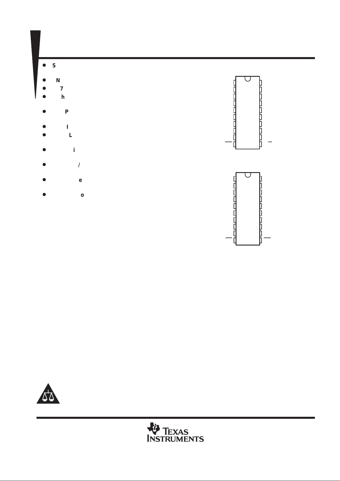
1
2
3
4
5
6
7
8
9
10
20
19
18
17
16
15
14
13
12
11
A1
A2
A3
A4
V
CC
A5
A6
A7
A8
CS
B1
B2
B3
B4
GND
B5
B6
B7
B8
T/R
SN75ALS057 . . . DW OR N PACKAGE
(TOP VIEW)
1
2
3
4
5
6
7
8
9
10
20
19
18
17
16
15
14
13
12
11
D1
R1
D2
R2
V
CC
D3
R3
D4
R4
TE
B1
E1
B2
E2
GND
B3
E3
B4
E4
RE
SN75ALS056 . . . DW OR N PACKAGE
(TOP VIEW)
†
The transceivers are suitable for IEEE Standard 896 applications to the extent of the operating conditions and characteristics specified in this
data sheet.
SN75ALS056, SN75ALS057
TRAPEZOIDAL-WAVEFORM INTERFACE BUS TRANSCEIVERS
SLLS028G – AUGUST 1987 – REVISED JUNE 1998
2
POST OFFICE BOX 655303 • DALLAS, TEXAS 75265
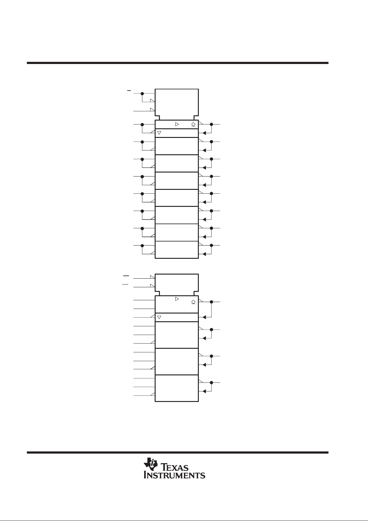
logic symbol
†
SN75ALS056
SN75ALS057
4
3
2
1
11
A4
A3
A2
A1
T/R
B4
B3
B2
B1
17
18
19
20
3EN1 (A-B)
3EN2 (B-A)
1
2
10
CS
G3
8
7
A7
A6
A5
B7
B6
B5
13
14
615
9
A8 B8
12
14
6
4
17
3
2
19
1
11
10
E3
D3
R2
E2
D2
R1
E1
D1
RE
TE
B3
B2
B1
15
18
20
EN1 (D-B)
EN2 (B-R)
1
2
B4
13
&
9
12
8
7
R4
E4
D4
R3
†
These symbols are in accordance with ANSI/IEEE Std 91-1984 and IEC Publication 617-12.

SN75ALS056, SN75ALS057
TRAPEZOIDAL-WAVEFORM INTERFACE BUS TRANSCEIVERS
SLLS028G – AUGUST 1987 – REVISED JUNE 1998
3
POST OFFICE BOX 655303 • DALLAS, TEXAS 75265
logic diagram (positive logic)
SN75ALS057
T/R
11
10
CS
1
A1
B1
20
Xmit
9
A8
B8
12
Rcv
B1
20
Rcv
Xmit
TE
10
RE
11
D1
1
E1
19
2
R1
9
12
8
R4
E4
D4
B4
13
SN75ALS056
†
These symbols are in accordance with ANSI/IEEE Std 91-1984 and IEC Publication 617-12.
SN75ALS056, SN75ALS057
TRAPEZOIDAL-WAVEFORM INTERFACE BUS TRANSCEIVERS
SLLS028G – AUGUST 1987 – REVISED JUNE 1998
4
POST OFFICE BOX 655303 • DALLAS, TEXAS 75265
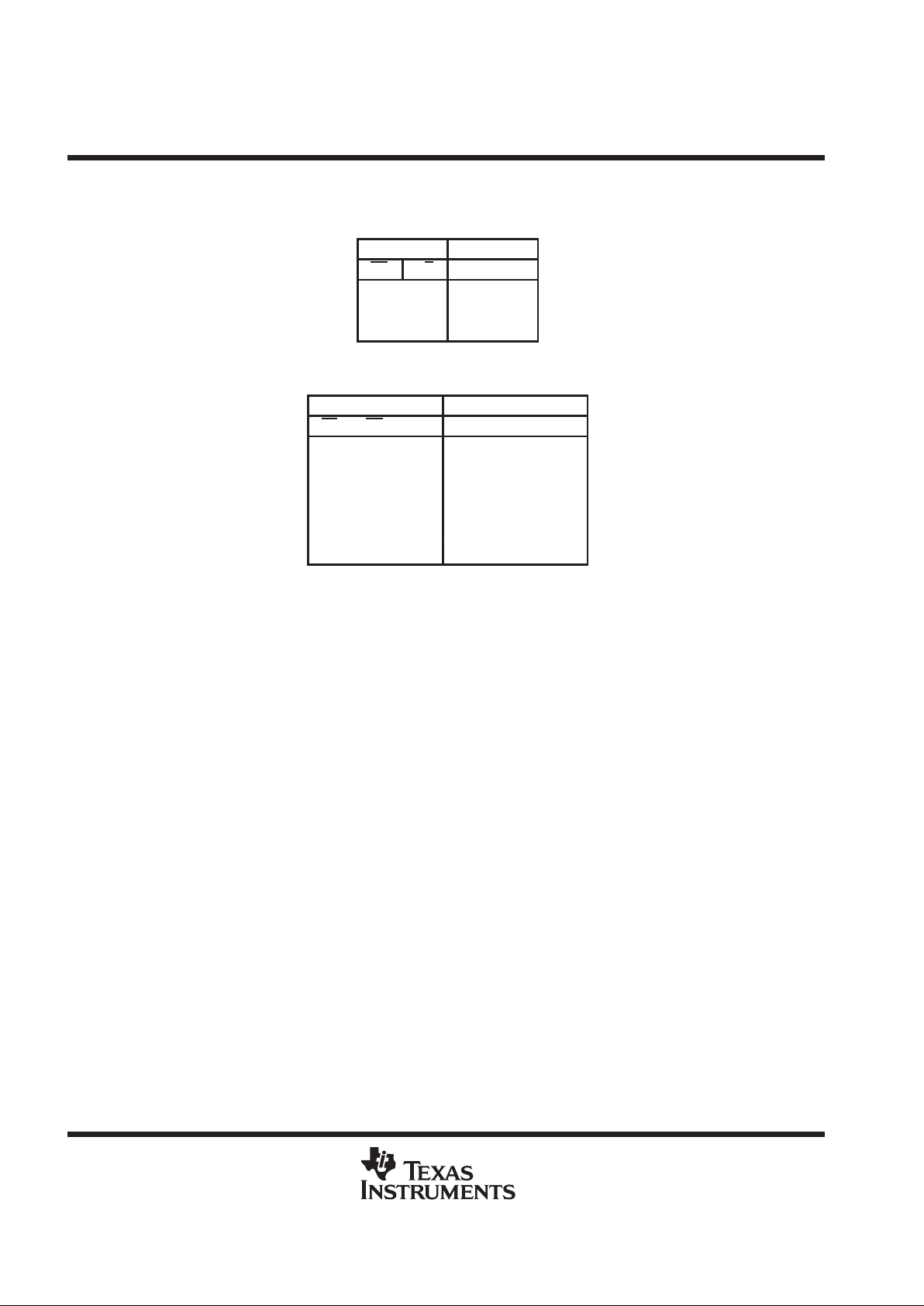
Function Tables
SN75ALS056
TRANSMIT/RECEIVE
CONTROLS
CHANNELS
CS T/R A ↔ B
L H T(A B)
L L R(B A)
H X D
SN75ALS057
TRANSMIT/RECEIVE
CONTROLS
CHANNELS
TE RE En D B B R
L L L D R
L LH T R
LHL D D
LHH T D
HLX D R
HHX D D
H = high level, L = low level, R = receive, T = transmit,
D = disable, X = irrelevant
Direction of data transmission is from An to Bn for the SN75ALS056 and from Dn to Bn for the SN75ALS057.
Direction of data reception is from Bn to An for the SN75ALS056 and from Bn to Rn for the SN75ALS057. Data
transfer is inverting in both directions.
SN75ALS056, SN75ALS057
TRAPEZOIDAL-WAVEFORM INTERFACE BUS TRANSCEIVERS
SLLS028G – AUGUST 1987 – REVISED JUNE 1998
5
POST OFFICE BOX 655303 • DALLAS, TEXAS 75265
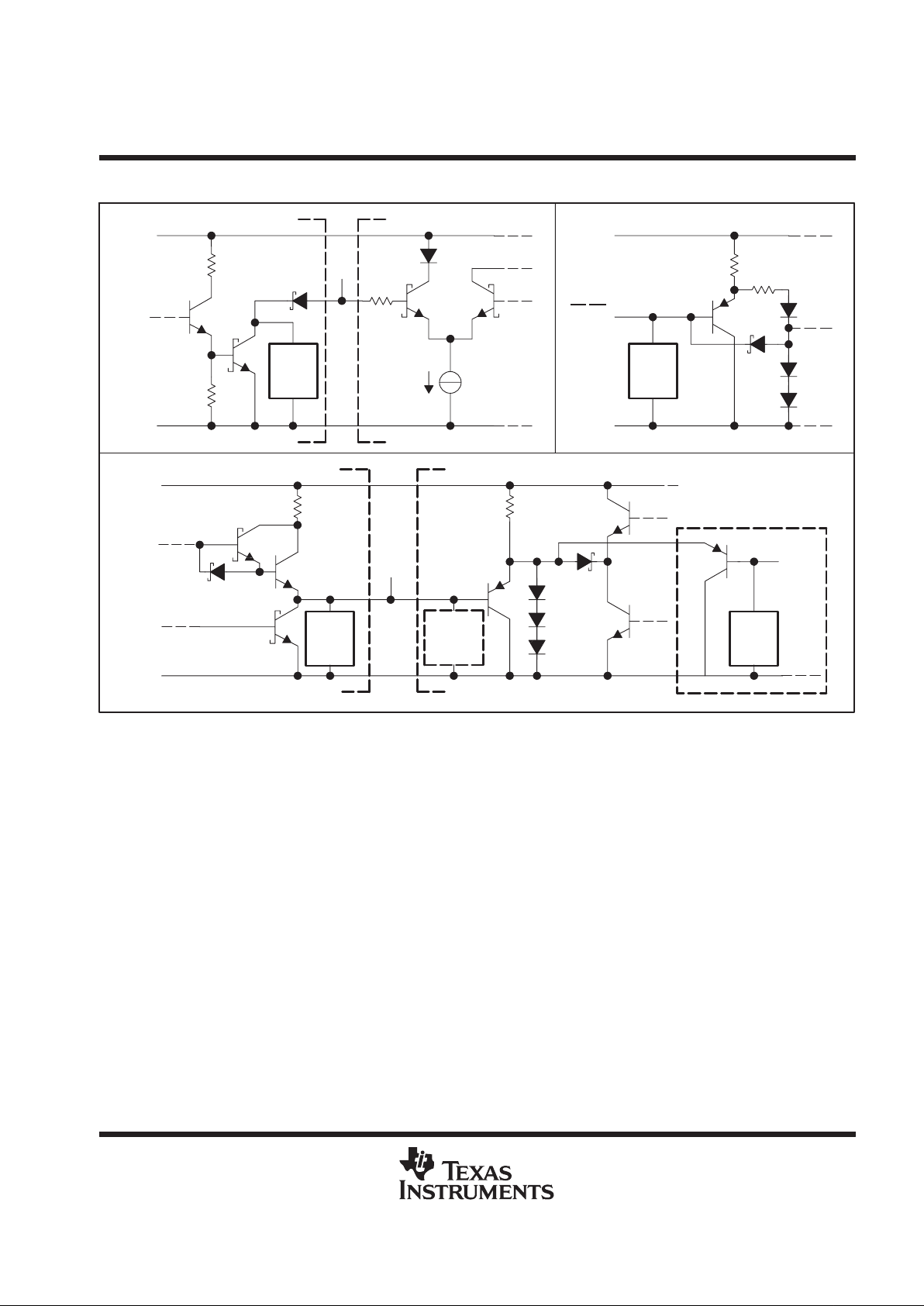
schematics of inputs and outputs
ESD
Protect
DRIVER OUTPUT RECEIVER INPUT CONTROL INPUTS
RECEIVER OUTPUT DRIVER INPUT
GND
Bn
V
CC
GND
40 µA
V
CC
GND
48 Ω 20 kΩ
An
or
Rn-Dn
SN75ALS057
Only
En
All resistor values shown are nominal.
17.5 kΩ
TE
/RE
Input
15 kΩ
2.5 kΩ
V
CC
ESD
Protect
ESD
Protect
ESD
Protect
ESD
Protect
†
†
Additional ESD protection is on the SN75ALS057, which has separate receiver-output and driver-input pins.
absolute maximum ratings over operating free-air temperature (unless otherwise noted)
‡
Supply voltage, V
CC
(see Note 1) 6 V. . . . . . . . . . . . . . . . . . . . . . . . . . . . . . . . . . . . . . . . . . . . . . . . . . . . . . . . . . . . .
Control input voltage, V
I
5.5 V. . . . . . . . . . . . . . . . . . . . . . . . . . . . . . . . . . . . . . . . . . . . . . . . . . . . . . . . . . . . . . . . . . .
Driver input voltage, V
I
5.5 V. . . . . . . . . . . . . . . . . . . . . . . . . . . . . . . . . . . . . . . . . . . . . . . . . . . . . . . . . . . . . . . . . . . .
Driver output voltage, V
O
2.5 V. . . . . . . . . . . . . . . . . . . . . . . . . . . . . . . . . . . . . . . . . . . . . . . . . . . . . . . . . . . . . . . . . .
Receiver input voltage, V
I
2.5 V. . . . . . . . . . . . . . . . . . . . . . . . . . . . . . . . . . . . . . . . . . . . . . . . . . . . . . . . . . . . . . . . . .
Receiver output voltage, V
O
5.5 V. . . . . . . . . . . . . . . . . . . . . . . . . . . . . . . . . . . . . . . . . . . . . . . . . . . . . . . . . . . . . . .
Continuous total power dissipation See Dissipation Rating Table. . . . . . . . . . . . . . . . . . . . . . . . . . . . . . . . . . . . .
Storage temperature range, T
stg
–65°C to 150°C. . . . . . . . . . . . . . . . . . . . . . . . . . . . . . . . . . . . . . . . . . . . . . . . . . .
Lead temperature 1,6 mm (1/16 inch) from case for 10 seconds: DW or N package 260 °C. . . . . . . . . . . . . . .
‡
Stresses beyond those listed under “absolute maximum ratings” may cause permanent damage to the device. These are stress ratings only, and
functional operation of the device at these or any other conditions beyond those indicated under “recommended operating conditions” is not
implied. Exposure to absolute-maximum-rated conditions for extended periods may affect device reliability.
NOTE 1: Voltage values are with respect to network ground terminal.

SN75ALS056, SN75ALS057
TRAPEZOIDAL-WAVEFORM INTERFACE BUS TRANSCEIVERS
SLLS028G – AUGUST 1987 – REVISED JUNE 1998
6
POST OFFICE BOX 655303 • DALLAS, TEXAS 75265
DISSIPATION RATING TABLE
PACKAGE
TA ≤ 25°C
POWER RATING
DERATING FACTOR
ABOVE TA = 25°C
TA = 70°C
POWER RATING
TA = 125°C
POWER RATING
DW 1025 mW 8.2 mW/°C 656 mW —
N 1150 mW 9.2 mW/°C 736 mW —
recommended operating conditions
MIN NOM MAX UNIT
Supply voltage, V
CC
4.75 5 5.25 V
High-level driver and control input voltage, V
IH
2 V
Low-level driver and control input voltage, V
IL
0.8 V
Bus termination voltage 1.9 2.1 V
Operating free-air temperature, T
A
0 70 °C
electrical characteristics over recommended ranges of supply voltage and operating free-air
temperature (unless otherwise noted)
SN75ALS056
PARAMETER
TEST CONDITIONS
†
MIN
TYP
†
MAX
UNIT
V
IK
Input clamp voltage at An, T/R, or CS II = –18 mA –1.5 V
V
IT
Receiver input threshold voltage at Bn 1.405 1.69 V
V
OH
High-level output voltage at An
Bn at 1.2 V, CS at 0.8 V,
T/R
at 0.8V , IOH = – 400 µA
2.4 V
An
Bn at 2 V ,CS at 0.8 V,
T/R
at 0.8 V, IOL = 16 mA
0.5
V
OL
Low-level output voltage
Bn
An at 2 V, CS at 0.8 V,
T/R
at 2 V, VL = 2 V,
RL =18.5 Ω,, See Figure 1
0.75 1.2
V
An, T/R or CS VI = V
CC
40
I
IH
High-level input current
Bn
VI = 2 V, VCC = 0 or 5.25 V,
An at 0.8 V , T/R
at 0.8 V
100
µA
I
IL
Low level input current at An, T/R, or CS VI = 0.4 V –400 µA
I
OS
Short-circuit output current at An
An at 0, Bn at 1.2 V ,
CS
at 0.8 V, T/R at 0.8 V
–40 –120 mA
I
CC
Supply current 75 mA
C
O(B)
Driver output capacitance 4.5 pF
†
Typical values are at VCC = 5 V, TA = 25°C.

SN75ALS056, SN75ALS057
TRAPEZOIDAL-WAVEFORM INTERFACE BUS TRANSCEIVERS
SLLS028G – AUGUST 1987 – REVISED JUNE 1998
7
POST OFFICE BOX 655303 • DALLAS, TEXAS 75265
electrical characteristics over recommended ranges of supply voltage and operating free-air
temperature (unless otherwise noted)
SN75ALS057
PARAMETER
TEST CONDITIONS
MIN TYP†MAX
UNIT
V
IK
Input clamp voltage at Dn, En, TE, or RE II = –18 mA –1.5 V
V
IT
Receiver input threshold voltage at Bn 1.41 1.69 V
V
OH
High-level output voltage at Rn
Bn at 1.2 V, RE at 0.8 V,
IOH = –400 µA
2.4 V
Rn
Bn at 2 V, RE at 0.8 V,
IOL = 16 mA
0.5
V
OL
Low-level output voltage
Bn
Dn at 2 V, En at 2 V,
TE
at 0.8 V , VL = 2 V,
RL = 18.5 Ω, See Figure 1
0.75 1.2
V
Dn, En,
TE
, or RE
VI = V
CC
40
I
IH
High-level input current
Bn
VI = 2 V, VCC = 0 or 5.25 V,
Dn at 0.8 V, En at 0.8 V ,
TE
at 0.8 V
100
µA
I
IL
Low-level input current at Dn, En, TE, or RE VI = 0.4 V –400 µA
I
OS
Short-circuit output current at Rn
Rn at 0, Bn at 1.2 V ,
RE
at 0.8 V
–40 –120 mA
I
CC
Supply current 40 mA
C
O(B)
Driver output capacitance 4.5 pF
†
Typical values are at VCC = 5 V, TA = 25°C.
switching characteristics over recommended ranges of supply voltage and operating free-air
temperature (unless otherwise noted)
PARAMETER
FROM
TO
TEST CONDITIONS
SN75ALS056
DRIVER
UNIT
(INPUT)
(OUTPUT)
MIN
TYP
†
MAX
t
PLH1
Propagation delay time,
low-to-high-level output
An and T/R at 2 V, VL = 2 V,
p
24
t
PHL1
Propagation delay time,
high-to-low-level output
CS
Bn
RL1
= 18 Ω,,
C
L
= 30 pF,
RL2 not connected, See Figure 2
20
ns
t
PLH2
Propagation delay time,
low-to-high-level output
CS at 0.8 V, T/R at 2 V ,
VL = 2 V, RL1 = 18 Ω,,
p
19
t
PHL2
Propagation delay time
high-to-low-level output
An
Bn
RL2
not connected,
C
L
= 30 pF,
See Figure 2,
18
ns
t
PLH3
Propagation delay time,
low-to-high-level output
V
I(An)
= 5 V, CS at 0.8 V,
RL1 = 18 Ω, CL = 30 pF,
25
t
PHL3
Propagation delay time,
high-to-low-level output
T/R
Bn
RL2 not connected, V
L
=
2 V
,
See Figure 3,
35
ns
t
TLH
Transition time,
low-to-high-level output
CS at 0.8 V, T/R at 2 V ,
V
= 2 V, C
= 30 pF,
1 3 11
t
THL
Transition time,
high-to-low-level output
An
Bn
L
,
L
,
RL1 = 18 Ω, RL2 not connected,
See Figure 2
1 3 6
ns
†
Typical values are at VCC = 5 V, TA = 25°C

SN75ALS056, SN75ALS057
TRAPEZOIDAL-WAVEFORM INTERFACE BUS TRANSCEIVERS
SLLS028G – AUGUST 1987 – REVISED JUNE 1998
8
POST OFFICE BOX 655303 • DALLAS, TEXAS 75265
switching characteristics over recommended ranges of supply voltage and operating free-air
temperature (unless otherwise noted)
PARAMETER
FROM
TO
TEST CONDITIONS
SN75ALS056
RECEIVER
UNIT
(INPUT)
(OUTPUT)
MIN MAX
t
PLH4
Propagation delay time,
low-to-high-level output
CS at 0.8 V, T/R at 0.8 V, R
1 = 390 Ω,
18
t
PHL4
Propagation delay time,
high-to-low-level output
Bn
An
,,
L
,
RL2 = 1.6 kΩ, CL = 30 pF, See Figure 4
18
ns
t
PLZ1
Output disable time from
low level
T/R An
CS at 0.8 V, V
I(Bn)
= 2 V, VL = 5 V,
RL1 = 390 Ω, RL2 not connected,
CL = 15 pF, See Figure 3
20 ns
t
PZL1
Output enable time to
low level
T/R An
CS at 0.8 V, V
I(Bn)
= 2 V, VL = 5 V,
RL1 = 390 Ω, RL2 = 1.6 kΩ,
CL = 30 pF, See Figure 3
40 ns
t
PHZ1
Output disable time from
high level
T/R An
CS at 0.8 V, V
I(Bn)
= 0, VL = 0,
RL1 = 390 Ω, RL2 not connected,
CL = 15 pF, See Figure 3
17 ns
t
PZH1
Output enable time to
high level
T/R An
CS at 0.8 V, VI
(Bn
) = 0, VL = 0,
RL1 not connected, RL2 = 1.6 kΩ,
CL = 30 pF, See Figure 3
15 ns
t
PLZ2
Output disable time from
low level
CS An
Bn at 2 V, T/R at 0.8 V , CL = 5 pF,
VL = 5 V, RL1 = 390 Ω,
RL2 not connected, See Figure 5
18 ns
t
PZL2
Output enable time to
low level
CS An
Bn at 2 V, T/R at 0.8 V , CL = 30 pF,
VL = 5 V, RL1 = 390 Ω, RL2 = 1.6 kΩ,
See Figure 5
15 ns
t
PHZ2
Output disable time from
high level
CS An
Bn at 0.8 V , T/R at 0.8 V, CL = 5 pF,
VL = 0, RL1 = 390 Ω,
RL2 not connected, See Figure 5
8 ns
t
PZH2
Output enable time to
high level
CS An
Bn at 0.8 V , T/R at 0.8 V, CL = 30 pF,
VL = 0, RL1 not connected,
RL2 = 1.6 kΩ, See Figure 5
17 ns
t
w(NR)
Receiver noise rejection
pulse duration
Bn An
CS at 0.8 V, T/R at 0.8 V, RL1 = 390 Ω,
RL2 = 1.6 kΩ, CL = 30 pF, VL = 5 V,
See Figure 6
3 ns

SN75ALS056, SN75ALS057
TRAPEZOIDAL-WAVEFORM INTERFACE BUS TRANSCEIVERS
SLLS028G – AUGUST 1987 – REVISED JUNE 1998
9
POST OFFICE BOX 655303 • DALLAS, TEXAS 75265
switching characteristics over recommended ranges of supply voltage and operating free-air
temperature (unless otherwise noted)
PARAMETER
FROM
TO
TEST CONDITIONS
SN75ALS057
DRIVER
UNIT
(INPUT)
(OUTPUT)
MIN
TYP
†
MAX
t
PLH1
Propagation delay time,
low-to-high-level output
Dn, En, RE at 2 V, VL = 2 V,
24
t
PHL1
Propagation delay time,
high-to-low-level output
TE
Bn
RL2
not connected,
RL1
= 18 Ω,
See Figure 2, CL = 30 pF
20
ns
t
PLH2
Propagation delay time,
low-to-high-level output
TE at 0.8 V, RE at 2 V,
V
= 2 V, R
1 = 18 Ω
,
19
t
PHL2
Propagation delay time,
high-to-low-level output
Dn or En
Bn
V
L
2 V,
RL1 18 Ω,
RL2 not connected,CL = 30 pF,
See Figure 2
18
ns
t
TLH
Transition time,
low-to-high-level output
RE at 2 V, VL = 2 V,
TE
at 0.8 V, RL1 = 18 Ω,,
1 3 11
t
THL
Transition time,
high-to-low-level output
Dn or En
Bn
,
L
,,
RL2 not connected, CL = 30 pF,
See Figure 2
1 3 6
ns
†
Typical values are at VCC = 5 V, TA = 25°C.
switching characteristics over recommended ranges of supply voltage and operating free-air
temperature (unless otherwise noted) (continued)
PARAMETER
FROM
TO
TEST CONDITIONS
SN75ALS057
RECEIVER
UNIT
(INPUT)
(OUTPUT)
MIN MAX
t
PLH4
Propagation delay time,
low-to-high-level output
RE at 0.8 V, TE at 2 V, VL = 5 V,
18
t
PHL4
Propagation delay time,
high-to-low-level output
Bn
Rn
RL1
=
390 Ω
,,
RL2
= 1.6 kΩ,,
C
L
= 30 pF,
See Figure 4
18
ns
t
PLZ2
Output disable time
from low level
RE
Rn
Bn at 2 V, TE at 2 V, VL = 5 V,
CL = 5 pF, RL1 = 390 Ω,
RL2 not connected, See Figure 5
18 ns
t
PZL2
Output enable time to
low level
RE
Rn
Bn at 2 V, TE at 2 V, VL = 5 V,
CL = 30 pF, RL1 = 390 Ω, RL2 = 1.6 kΩ,
See Figure 5
15 ns
t
PHZ2
Output disable time
from high level
RE
Rn
Bn at 0.8 V , TE at 2 V, VL = 0,
CL = 5 pF, RL1 = 390 Ω,
RL2 not connected, See Figure 5
17 ns
t
PZH2
Output enable time to
high level
RE
Rn
Bn at 0.8 V , TE at 2 V, VL = 0,
CL = 30 pF, RL1 not connected,
RL2 = 1.6 kΩ, See Figure 5
17 ns
t
w(NR)
Receiver noise
rejection pulse duration
Bn Rn
TE at 2 V, RE at 0.8 V , VL = 0,
RL1 = 390 Ω, RL2 = 1.6 kΩ, CL = 30 pF,
See Figure 6
3 ns

SN75ALS056, SN75ALS057
TRAPEZOIDAL-WAVEFORM INTERFACE BUS TRANSCEIVERS
SLLS028G – AUGUST 1987 – REVISED JUNE 1998
10
POST OFFICE BOX 655303 • DALLAS, TEXAS 75265
switching characteristics over recommended ranges of supply voltage and operating free-air
temperature (unless otherwise noted) (continued)
PARAMETER
FROM
(INPUT)TO(OUTPUT)
TEST CONDITIONS
SN75ALS057
DRIVER PLUS
RECEIVER
UNIT
()
()
MIN MAX
t
PLH6
Propagation delay time,
low-to-high-level output
RE at 0.8 V, TE at 0.8 V, RL1 = 390 Ω,
40
t
PHL6
Propagation delay time,
high-to-low-level output
Dn
Rn
L
RL2 = 1.6 kΩ,, CL = 30 pF, See Figure 7
40
ns
PARAMETER MEASUREMENT INFORMATION
V
L
V
O
(Bn)
SN75ALS056
or
SN75ALS057
RL1
Figure 1. Driver Low-Level-Output-Voltage Test Circuit

SN75ALS056, SN75ALS057
TRAPEZOIDAL-WAVEFORM INTERFACE BUS TRANSCEIVERS
SLLS028G – AUGUST 1987 – REVISED JUNE 1998
11
POST OFFICE BOX 655303 • DALLAS, TEXAS 75265
PARAMETER MEASUREMENT INFORMATION
TEST CIRCUIT
VOLTAGE WAVEFORMS
CS
, TE
1.5 V
t
PHL1
1.5 V
t
PHL2
t
THL
90%
1.55 V
10%
t
PLH1
3 V
0
3 V
0
(An, Dn, En)
V
OH
V
OL
V
O(Bn)
90%
t
TLH
10%
1.55 V
1.5 V
1.5 V
V
I
(Bn)
RL1
V
O
V
L
CL (includes jig capacitance)
SN75ALS056
or
SN75ALS057
V
I(CS, TE, An, Dn, En)
t
PLH2
RL2
NOTE A: tr = tf ≤ 5 ns from 10% to 90%
Figure 2. Driver Test Circuit and Voltage Waveforms

SN75ALS056, SN75ALS057
TRAPEZOIDAL-WAVEFORM INTERFACE BUS TRANSCEIVERS
SLLS028G – AUGUST 1987 – REVISED JUNE 1998
12
POST OFFICE BOX 655303 • DALLAS, TEXAS 75265
PARAMETER MEASUREMENT INFORMATION
TEST CIRCUIT
VOLTAGE WAVEFORMS
RL2
V
L
RL1
O
V
CL (includes jig capacitance)
(Bn,An)
SN75ALS056
V
I(T/R)
V
I(An, Bn)
1.55 V
1.5 V
1.55 V
1.5 V
t
PZH1
t
PZL1
t
PLH3
1.5 V
3 V
0
t
PHL3
V
I(T/R)
1.5 V
t
PLZ1
t
PHZ1
0.5 V
0.5 V
V
O(Bn)
V
O(An)
V
O(An)
5 V
15 pF
390 Ω
S1
S1 Closed
S2 Open
S1 Open
S2 Closed
S2
1.6 kΩ
NOTE A: tr = tf ≤ 5 ns from 10% to 90%
Figure 3. Propagation Delay From T/R to An or Bn Test Circuit and Voltage Waveforms

SN75ALS056, SN75ALS057
TRAPEZOIDAL-WAVEFORM INTERFACE BUS TRANSCEIVERS
SLLS028G – AUGUST 1987 – REVISED JUNE 1998
13
POST OFFICE BOX 655303 • DALLAS, TEXAS 75265
TEST CIRCUIT
VOLTAGE WAVEFORMS
t
PHL4
1.55 V
1.5 V
V
O(An, Rn)
V
I(Bn)
V
OL
V
OH
1 V
2 V
1.5 V
t
PLH4
1.55 V
CL (includes jig capacitance)
(An,Rn)
V
O
5 V
V
I(Bn)
RL2
RL1
SN75ALS056
or
SN75ALS057
NOTE A: tr = tf ≤ 5 ns from 10% to 90%
Figure 4. Receiver Test Circuit and Voltage Waveforms
TEST CIRCUIT
VOLTAGE WAVEFORMS
t
PZH2
t
PZL2
1.5 V
1.5 V
1.5 V
0.5 V
0.5 V
t
PLZ2
t
PHZ2
1.5 V
0
3 V
V
O(An, Rn)
V
L
RL1
RL2
CL (includes jig capacitance)
(An,Rn)
V
O
V
I(CS, RE)
SN75ALS056
or
SN75ALS057
V
O(An, Rn)
V
I(CS, RE)
NOTE A: tr = tf ≤ 5 ns from 10% to 90%
Figure 5. Propagation Delay From CS to An or RE to Rn Test Circuit and Voltage Waveforms

SN75ALS056, SN75ALS057
TRAPEZOIDAL-WAVEFORM INTERFACE BUS TRANSCEIVERS
SLLS028G – AUGUST 1987 – REVISED JUNE 1998
14
POST OFFICE BOX 655303 • DALLAS, TEXAS 75265
PARAMETER MEASUREMENT INFORMATION
TEST CIRCUIT
Bus Logic
Low Level
tw is increased until the output voltage
fall just reaches 2 V .
High Level
Bus Logic
tw is increased until the output voltage rise
just reaches 0.8 V .
VOLTAGE WAVEFORMS
1.25 V
2 V
1.55 V
t
w(NR)
t
w(NR)
1.55 V
V
1
1.85 V
1.1 V
(An, Rn)
5 V
V
O
SN75ALS057
or
SN75ALS056
V
I(Bn)
RL1
RL2
CL (includes jig capacitance)
NOTE A: tr = tf ≤ 5 ns from 10% to 90%
Figure 6. Receiver Noise-Immunity Test Circuit and Voltage Waveforms
TEST CIRCUIT
VOLTAGE WAVEFORMS
t
PHL6
1.5 V
1.5 V
t
PLH6
1.5 V
1.5 V
V
O(Rn)
0
3 V
V
I(Dn)
30 pF
2 V
18 Ω
(Rn)
5 V
V
O
SN75ALS057
(Bn)
RL1
RL2
CL (includes jig capacitance)
V
I(Dn)
NOTE A: tr = tf ≤ 5 ns from 10% to 90%
Figure 7. Driver Plus Receiver Delay-Times Test Circuits and Voltage Waveforms

IMPORTANT NOTICE
T exas Instruments and its subsidiaries (TI) reserve the right to make changes to their products or to discontinue
any product or service without notice, and advise customers to obtain the latest version of relevant information
to verify, before placing orders, that information being relied on is current and complete. All products are sold
subject to the terms and conditions of sale supplied at the time of order acknowledgement, including those
pertaining to warranty, patent infringement, and limitation of liability.
TI warrants performance of its semiconductor products to the specifications applicable at the time of sale in
accordance with TI’s standard warranty. Testing and other quality control techniques are utilized to the extent
TI deems necessary to support this warranty. Specific testing of all parameters of each device is not necessarily
performed, except those mandated by government requirements.
CERT AIN APPLICATIONS USING SEMICONDUCTOR PRODUCTS MAY INVOLVE POTENTIAL RISKS OF
DEATH, PERSONAL INJURY, OR SEVERE PROPERTY OR ENVIRONMENTAL DAMAGE (“CRITICAL
APPLICATIONS”). TI SEMICONDUCTOR PRODUCTS ARE NOT DESIGNED, AUTHORIZED, OR
WARRANTED TO BE SUITABLE FOR USE IN LIFE-SUPPORT DEVICES OR SYSTEMS OR OTHER
CRITICAL APPLICATIONS. INCLUSION OF TI PRODUCTS IN SUCH APPLICA TIONS IS UNDERST OOD TO
BE FULLY AT THE CUSTOMER’S RISK.
In order to minimize risks associated with the customer’s applications, adequate design and operating
safeguards must be provided by the customer to minimize inherent or procedural hazards.
TI assumes no liability for applications assistance or customer product design. TI does not warrant or represent
that any license, either express or implied, is granted under any patent right, copyright, mask work right, or other
intellectual property right of TI covering or relating to any combination, machine, or process in which such
semiconductor products or services might be or are used. TI’s publication of information regarding any third
party’s products or services does not constitute TI’s approval, warranty or endorsement thereof.
Copyright 1998, Texas Instruments Incorporated
 Loading...