

SCSI DIFFERENTIAL CONVERTER-DATA
SLLS322A – NOVEMBER 1999 – REVISED JANUARY 2000
D
Provides High-Voltage Differential SCSI
From Single-Ended Controller When Used
With the SN75970B Control Transceiver
D
Meets or Exceeds the Requirements of EIA
Standard RS-485 and ISO-8482 Standards
D
ESD Protection on Bus Pins to 12 kV
D
Packaged in Shrink Small-Outline Package
with 25 mil Terminal Pitch and Thin
Small-Package with 20 mil Terminal Pitch
D
Low Disabled-Supply Current 32 mA Typ
D
Thermal Shutdown Protection
D
Positive- and Negative-Current Limiting
D
Power-Up/-Down Glitch Protection
D
Open-Circuit Failsafe Receivers
description
The SN75971B SCSI differential converter-data is a
9-channel RS-485 transceiver. When used in conjunction with its companion control transceiver, the
SN75970B, the resulting chip set provides the superior
electrical performance of differential SCSI from a
single-ended SCSI bus or controller. A 16-bit
Ultra-SCSI (or Fast-20) SCSI bus can be implemented
with just three devices (two data and one control) in the
space efficient, 56-pin, shrink small-outline package
(SSOP) or thin shink small outline package (TSSOP)
and a few external components. An 8-bit SCSI bus
requires only one data and one control transceiver.
The SN75971B is available in a B2 (20 Mxfer)
version and a B1 (10 Mxfer) version.
In a typical differential SCSI node, the SCSI controller
provides an enable for each external RS-485
transceiver channel. This could require as many as 27
extra terminals for a 16-bit differential bus controller or relegate a 16-bit, single-ended controller to only an 8-bit
differential bus. Using the standard nine SCSIcontrol signals, the SN75970B control transceiver decodes the
state of the bus and enables the SN75971B data transceiver to transmit the single-ended SCSI input signals
(A side) differentially to the cable or receive the differential cable signals (B side) and drive the single-ended
outputs to the controller.
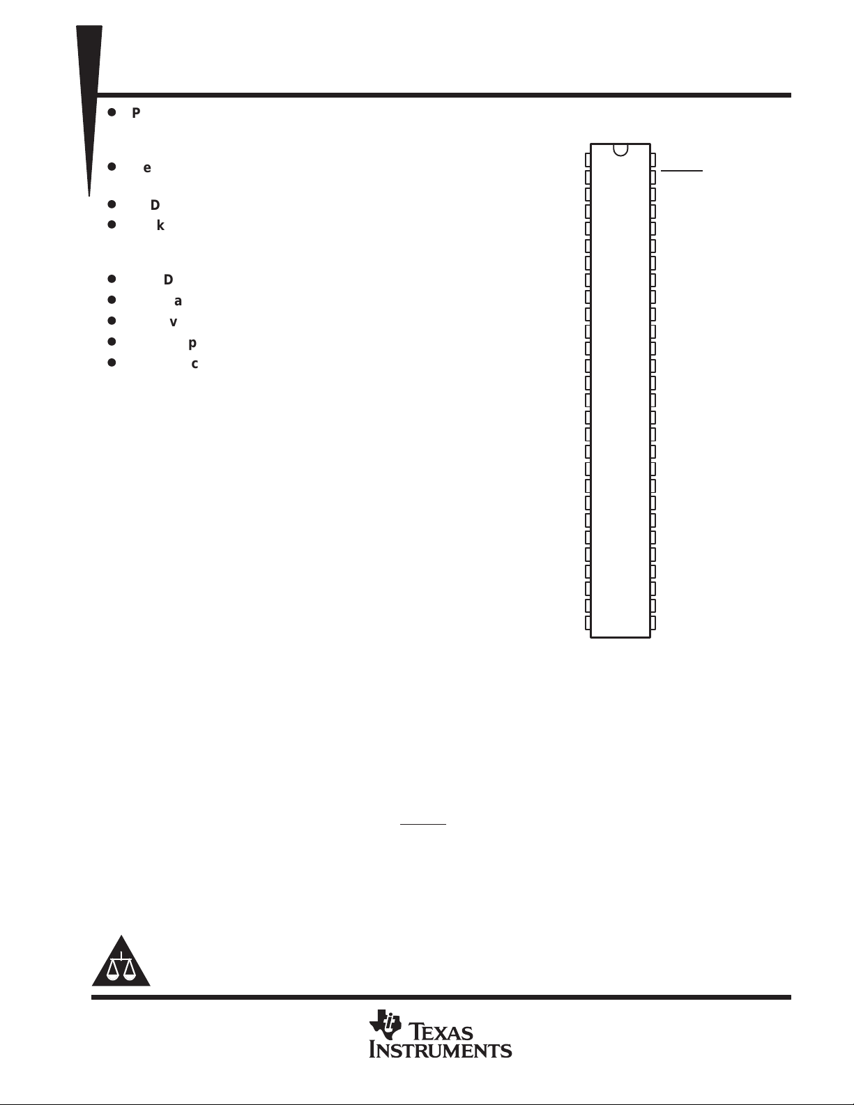
DGG OR DL PACKAGE
(TOP VIEW)
SDB
DRVBUS
GND
ADBP–
ADB7–
ADB6–
ADB5–
GND
GND
GND
GND
GND
ABD4–
ADB3–
ADB2–
ADB1–
ADB0–
Pins 13 – 17 and 40 – 44 are connected
together to the package lead frame and
to signal ground.
NC – No internal connection
V
V
NC
NC
NC
NC
CC
CC
NC
NC
NC
NC
NC
1
2
3
4
5
6
7
8
9
10
11
12
13
14
15
16
17
18
19
20
21
22
23
24
25
26
27
28
56
55
54
53
52
51
50
49
48
47
46
45
44
43
42
41
40
39
38
37
36
35
34
33
32
31
30
29
DSENS
RESET
GND
BDBP–
BDBP+
BDB7–
BDB7+
BDB6–
BDB6+
BDB5–
BDB5+
V
CC
GND
GND
GND
GND
GND
V
CC
BDB4–
BDB4+
BDB3–
BDB3+
BDB2–
BDB2+
BDB1–
BDB1+
BDB0–
BDB0+
SN75971B
A reset function, which disables all outputs and clears internal latches, can be accomplished from two external
inputs and two internally-generated signals. RESET
(reset) and DSENS (differential sense) are available to
external circuits for a bus reset or to disable all outputs should a single-ended cable be inadvertently connected
to a differential connector . Internally-generated power-up and thermal-shutdown signals have the same affect
when the supply voltage is below approximately 3.5 V or the junction temperature exceeds 175°C.
Please be aware that an important notice concerning availability, standard warranty, and use in critical applications of
Texas Instruments semiconductor products and disclaimers thereto appears at the end of this data sheet.
PRODUCTION DATA information is current as of publication date.
Products conform to specifications per the terms of Texas Instruments
standard warranty. Production processing does not necessarily include
testing of all parameters.
POST OFFICE BOX 655303 • DALLAS, TEXAS 75265
Copyright 2000, Texas Instruments Incorporated
1
SN75971B
I/O
DESCRIPTION
SCSI DIFFERENTIAL CONVERTER-DATA
SLLS322A – NOVEMBER 1999 – REVISED JANUARY 2000
description (continued)
The SCSI, differential, converter-data chip operates in two modes depending on the state of the DRVBUS input.
With DRVBUS low , a bidirectional latch circuit sets the direction of data transfer. Each data bit has its own latch,
and each bit’s direction is independent of all other bits. When neither the single-ended nor the differential sides
are asserted, the latch disables both A- and B-side output drivers. When the input to either side is asserted, the
latch enables the opposite side’s driver and sets data flow from the asserted input to the opposite side of the
device. When the input deasserts, the latch maintains the direction until the receiver on the enabled driver
detects a deassertion. The latch then returns to the initial state. No parity checking is done by this device; the
parity signal passes through the device like other data signals do.
When DRVBUS is high, direction is determined by the SDB signal. However , a change in SDB does not always
immediately change the direction. When DRVBUS first asserts, the direction indicated by SDB is latched and
takes effect immediately . When SDB changes while DRVBUS is high, the drivers that were on immediately turn
off. However , the other driver set does not turn on until the receivers sense a deasserted state on all nine data
lines. This is done to prevent the active drivers from turning on until all other drivers are off and the terminators
pull the lines to a deasserted state.
The single-ended SCSI bus interface consists of CMOS, bidirectional inputs and outputs. The drivers are rated
to ±16 mA of output current. The receiver inputs are pulled high with approximately 4 mA to eliminate the need
for external pullup resistors for the open-drain outputs of most single-ended SCSI controllers. The single-ended
side of the device is not intended to drive the SCSI bus directly.
The differential SCSI bus interface consists of bipolar , bidirectional inputs and outputs that meet or exceed the
requirements of EIA-485 and ISO 8482-1982/TIA TR30.2 referenced by American National Standard of
Information Systems (ANSI) X3.131-1994 Small Computer System Interface-2 (SCSI-2) and SCSI-3 Fast-20
Parallel Interface (Fast-20) X3.277:1996.
The SN75971B is characterized for operation over the temperature range of 0°C to 70°C.
Terminal Functions
TERMINAL
NAME NO.
ADBn–, where
n = {0,1,2,3,4,5,6,7,P}
BDBn+, where
n = {0,1,2,3,4,5,6,7,P}
BDBn–, where
n = {0,1,2,3,4,5,6,7,P}
DRVBUS 2 Input, TTL levels,
DSENS 56 Input, TTL levels,
RESET 55 Input, TTL levels,
SDB 1 Input, TTL levels,
4, 6, 8, 10, 19,
21, 23, 25, 27
29, 31, 33, 35,
37, 46, 48, 50, 52
30, 32, 34, 36,
38,47, 49, 51, 53
I/O, Single-ended
SCSI voltage levels,
Strong pullup
I/O, RS-485,
Weak pulldown
I/O, RS-485,
Weak pulldown
Weak pulldown
Weak pullup
Weak pullup
Weak pulldown
Bidirectional I/O for data and parity bits to and from the single-ended SCSI
controller. As outputs, these terminals can source or sink 16 mA. As inputs,
they are pulled up with about 4-mA to eliminate external resistors.
Bidirectional I/O for data and parity to and from the differential SCSI bus.
Bidirectional I/O for the complement of data and parity to and from the
differential SCSI bus.
A high-level logic signal from the control transceiver enables either the
single-ended or differential drivers as directed by SDB.
A low-level input initializes the internal latches and disables all drivers.
A low-level input initializes the internal latches and disables all drivers.
A high-level logic signal from the control transceiver sends data from the
differential bus to the single-ended bus. A low-level signal reverses the
flow.
2
POST OFFICE BOX 655303 • DALLAS, TEXAS 75265
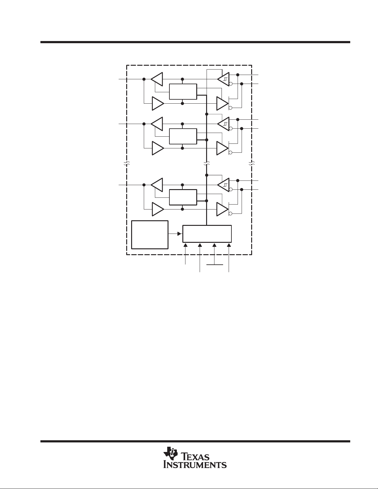
functional block diagram
ADBP–
ADB7–
ADB0–
4
6
27
SN75971B
Control
Latch
Control
Latch
Control
Latch
SN75971B
SCSI DIFFERENTIAL CONVERTER-DATA
SLLS322A – NOVEMBER 1999 – REVISED JANUARY 2000
53
BDBP–
52
BDBP+
51
BDB7–
50
BDB7+
(6 Identical Channels
Not Shown)
30
BDB0–
29
BDB0+
Power-Up
and Thermal
Shut-Down
Circuits
Steering and
Control Logic
2 1 55 56
DRVBUS
RESET
SDB
DSENS
POST OFFICE BOX 655303 • DALLAS, TEXAS 75265
3
SN75971B
SCSI DIFFERENTIAL CONVERTER-DATA
SLLS322A – NOVEMBER 1999 – REVISED JANUARY 2000
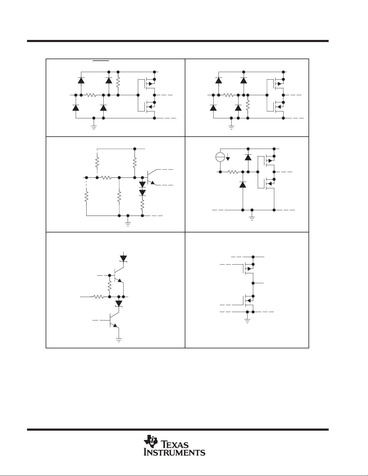
schematics of inputs and outputs
Input
100 kΩ
(B– Pin Only)
Input
100 kΩ
(B+ Pin Only)
, AND DSENS
RESET
200 Ω
B+ AND B– Inputs
18 kΩ
B+ AND B– Outputs
22 kΩ
12 kΩ
V
CC
3 kΩ
V
1 kΩ
CC
SDB AND DRVBUS
V
CC
Input
Input
200 Ω
50 kΩ
A
4 mA
200 Ω
A
V
CC
V
CC
V
CC
B+
B–
Output
18 kΩ
Output
4
POST OFFICE BOX 655303 • DALLAS, TEXAS 75265
SN75971B
SCSI DIFFERENTIAL CONVERTER-DATA
SLLS322A – NOVEMBER 1999 – REVISED JANUARY 2000
absolute maximum ratings over operating free-air temperature range (unless otherwise noted)
Supply voltage range, VCC (see Note 1) –0.3 V to 7 V. . . . . . . . . . . . . . . . . . . . . . . . . . . . . . . . . . . . . . . . . . . . . .
Differential bus voltage range (B side) –10 V to 15 V. . . . . . . . . . . . . . . . . . . . . . . . . . . . . . . . . . . . . . . . . . . . . . . .
Single-ended bus voltage range (A side and control inputs) –0.3 V to 7 V. . . . . . . . . . . . . . . . . . . . . . . . . . . . . .
Continuous total power dissipation (see Note 2) Internally Limited (see Dissipation Rating Table). . . . . . . . . .
Electrostatic discharge (see Note 3): Class 2 A (all pins) 4 kV. . . . . . . . . . . . . . . . . . . . . . . . . . . . . . . . . . . . . . .
Class 2 B (all pins) 400 V. . . . . . . . . . . . . . . . . . . . . . . . . . . . . . . . . . . . . .
Class 3 A (B-side and GND) 12 kV. . . . . . . . . . . . . . . . . . . . . . . . . . . . . .
Class 3 B (B-side and GND) 400 V. . . . . . . . . . . . . . . . . . . . . . . . . . . . . .
Operating free-air temperature range, T
Storage temperature range, T
65°C to 150°C. . . . . . . . . . . . . . . . . . . . . . . . . . . . . . . . . . . . . . . . . . . . . . . . . . . .
stg
Lead temperature 1,6 mm (1/16 inch) from case for 10 seconds 260°C. . . . . . . . . . . . . . . . . . . . . . . . . . . . . . .
†
Stresses beyond those listed under “absolute maximum ratings” may cause permanent damage to the device. These are stress ratings only, and
functional operation of the device at these or any other conditions beyond those indicated under “recommended operating conditions” is not
implied. Exposure to absolute-maximum-rated conditions for extended periods may affect device reliability.
NOTES: 1. All voltage values are with respect to GND.
2. The maximum operating junction temperature is internally limited. Use the dissipation rating table to operate below this temperature.
3. This absolute maximum rating is tested in accordance with MIL-STD-883C, Method 3015.7.
PACKAGE
DGG 3333 mW 26.7 mW/°C 2133 mW
DL 3709 mW 29.7 mW/°C 2374 mW
‡
This is the inverse of the traditional junction-to-case thermal resistance (R
High-K (per JEDEC) PCB installations.
POWER RATING
0°C to 70°C. . . . . . . . . . . . . . . . . . . . . . . . . . . . . . . . . . . . . . . . . . . . . .
A
DISSIPATION RATING TABLE
TA ≤ 25°C
DERATING FACTOR
ABOVE TA = 25°C
‡
TA = 70°C
POWER RATING
θJA
) for
†
recommended operating conditions
Supply voltage, V
High-level input voltage, V
Low-level input voltage, V
Voltage at any bus terminal (separately or common-mode), VO or V
High-level output current, I
Low-level output current, I
Operating case temperature, T
Operating free-air temperature, T
CC
IH
IL
OH
OL
C
A
MIN NOM MAX UNIT
4.75 5 5.25 V
A side and control 2 V
A side and control 0.8 V
I
B side
A side –16 mA
A side 16 mA
0 125 °C
0 70 °C
12
–7
V
POST OFFICE BOX 655303 • DALLAS, TEXAS 75265
5

SN75971B
V
g
V
VOLLow-level output voltage
V
V
Other input at 0 V
mA
IIBus input current
B or B
V
Other input at 0 V
mA
A
A
A side
out ut current
C
P
‡
SCSI DIFFERENTIAL CONVERTER-DATA
SLLS322A – NOVEMBER 1999 – REVISED JANUARY 2000
electrical characteristics over recommended operating conditions (unless otherwise noted)
PARAMETER TEST CONDITIONS MIN TYP†MAX UNIT
V
OD(H)
V
OD(L)
OH
V
IT+
V
IT–
V
hys
I
IH
I
IL
I
OS
I
OZ
I
CC
C
O
pd
†
All typical values are at VCC = 5 V, TA = 25°C.
‡
Cpd determines the no-load dynamic current consumption, IS = Cpd × VCC × f + I
§
The algebraic convention with the least positive (more negative) limit is designated minimum, is used in this data sheet for the differential input
voltage only .
Driver high-level differential output voltage See Figure 1 –1 –2.2 V
Driver low-level differential output voltage See Figure 1 1 1.8 V
High-level output
voltage
p
Receiver positive-going
differential input
threshold voltage
Receiver negative-going
differential input
threshold voltage
Receiver input
hysteresis voltage (V
– V
)
IT–
p
High-level input current
Low-level input current
Short-circuit output
current
High-impedance-state
p
Supply current
Output capacitance VI = 0.6 sin(2π × 106t) + 1.5 V, BDBn to GND 18 21 pF
ower dissipation capacitance
A side VID = –200 mV, IOH = –16 mA 2.5 4.2
B side
A side VID = 200 mV, IOL = 16 mA 0.4 0.8
B side IOL = 60 mA 1.6
B side
IT+
A side –2 –5 –8 mA
RESET
, DSENS
SDB, DRVBUS 25
A side –6 –9 mA
RESET
, DSENS
SDB, DRVBUS ±30
B side VO = 5 V and 0 ±250 mA
B side See I
Disabled RESET at 0.8 V, Others open 38 46
B to A
Enabled
A to B
Enabled
IOH = –60 mA 3.4
IOH = –16 mA See Figure 2 0.2 V
IOL = 16 mA See Figure 2 –0.2
= 12 V,
I
= –7 V,
I
VIH = 2 V
VIL = 0.8 V
SDB and DRVBUS at 2 V,
All other inputs open,
SDB at 0.8 V,
All other inputs open,
B to A, One channel 40 pF
A to B, One channel 100 pF
p
p
VCC = 5 V 0.6 1
VCC = 0 0.7 1
VCC = 5 V –0.5 –0.8
VCC = 0 –0.4 –0.8
VID = –1 V,
No load
DRVBUS at 2 V,
No load
CC.
§
35 45 mV
–70 –100
–66 –100
–2 –5 –8
–6 –9
I
39 50
32 66
µ
µ
mA
V
6
POST OFFICE BOX 655303 • DALLAS, TEXAS 75265

SN75971B
t
t
y, ,g
t
t
y, ,g
ns
SN75971B1
t
Sk
t
†
ns
SN75971B2
SCSI DIFFERENTIAL CONVERTER-DATA
SLLS322A – NOVEMBER 1999 – REVISED JANUARY 2000
switching characteristics over recommended of operating conditions (unless otherwise noted)
PARAMETER TEST CONDITIONS MIN MAX UNIT
See Figures 3 and 4 3 14
SN75971B1
Delay time, A to B, high- to low-
,
d1
d2
level or low- to high-level output
SN75971B2
SN75971B1
Delay time, B to A, high- to low-
,
d3
d4
level or low- to high-level output
SN75971B2
p
sk(pp)
t
sk(p)
t
dis1
t
dis2
t
en1
t
en2
t
en(TX)
†
Part-to-part skew is the magnitude of the difference in propagation delay times between any two devices when both operate with the same supply
voltages, the same temperature, and the same loads.
‡
Pulse skew is the difference between the high-to-low and low-to-high propagation delay times of any single channel.
ew, part-to-par
Pulse skew
Disable time, A to B See Figures 3 and 4 200 ns
Disable time, B to A See Figures 5 and 6 35 ns
Enable time, A to B See Figures 3 and 4 65 ns
Enable time, B to A See Figures 5 and 6 65 ns
Enable time, receive-to-transmit See Figure 7 142 ns
p
‡
VCC = 5 V, TA = 25°C, See Figures 3 and 4 4 12
VCC = 5 V, TA = 70°C, See Figures 3 and 4 4.9 12.9
See Figures 3 and 4 5 12
VCC = 5 V, TA = 25°C, See Figures 3 and 4 6.2 10.2
VCC = 5 V, TA = 70°C, See Figures 3 and 4 6.9 10.9
See Figures 5 and 6 5.4 18.1
VCC = 5 V, TA = 25°C, See Figures 5 and 6 6.5 15.4
VCC = 5 V, TA = 70°C, See Figures 5 and 6 7.2 16.1
See Figures 5 and 6 7.7 15
VCC = 5 V, TA = 25°C, See Figures 5 and 6 8.7 13.2
VCC = 5 V, TA = 70°C, See Figures 5 and 6 9.4 13.9
A to B See Figures 5 and 6 8
B to A See Figures 5 and 6 9
A to B See Figures 5 and 6 4
B to A See Figures 5 and 6 5
ns
4 ns
POST OFFICE BOX 655303 • DALLAS, TEXAS 75265
7

SN75971B
SCSI DIFFERENTIAL CONVERTER-DATA
SLLS322A – NOVEMBER 1999 – REVISED JANUARY 2000
PARAMETER MEASUREMENT INFORMATION
2 V or 0.8 V
ADBn–
VIH, V
IL
BDBn–
BDBn+
165 Ω
5 V
75 Ω
165 Ω
VOH, V
V
OD
VOH, V
OL
OL
NOTES: A. Resistance values are in ohms with a tolerance of ± 5%.
B. All input voltage levels are held to within 0.01 V.
C. The logical function is set with SDB at 0.8 V, DRVBUS at 3.5 V, and all others left open.
Figure 1. Differential Driver VOD, VOH, and VOL Test Circuit
BDBn–
I
I
NOTES: A. Resistance values are in ohms with a tolerance of ± 5%.
B. All input voltage levels are held to within 0.01 V.
C. The logical function is set with SDB and DRVBUS at 3.5 V , and all others left open.
VID or V
V
I
IT
BDBn+
Figure 2. Single-Ended Driver VOH, VOL, V
ADBn–
VOL or V
IT+
OL
, and V
IOH or I
OL
Test Circuit
IT–
8
POST OFFICE BOX 655303 • DALLAS, TEXAS 75265

SCSI DIFFERENTIAL CONVERTER-DATA
SLLS322A – NOVEMBER 1999 – REVISED JANUARY 2000
PARAMETER MEASUREMENT INFORMATION
SN75971B
GND
AB
S2
tent
S1
165 Ω
375 Ω
50%
d
tdt
dis
B+
I
I
I
Input
(see Note A)
3 V
1.5 V
0 V
NOTES: A. The input pulse is supplied by a generator having the following characteristics: PRR ≤ 1 MHz, 45% < duty cycle < 50%, tr ≤ 1 ns,
tf ≤ 1 ns, ZO=50Ω.
B. CL includes probe and jig capacitance.
C. Resistance values are in ohms with a tolerance of ± 5%.
D. All input voltage levels are held to within 0.01 V.
A
V
I
Input Output
t
0
O
V
OD
V
I
O
B–
V
O
~ –0.925 V
t0or
O
V
OD(H)
V
OD(L)
15 pF
75 Ω
15 pF
165 Ω
375 Ω
5 V
0.5 V
Figure 3. A to B Propagation Delay Time Test Circuit
SDB
DSENS
RESET
ADBn–
DRVBUS
BDBn–
BDBn+
V
OD
t
d1
t
d2
t
en1
t
dis1
Figure 4. A to B Timing Waveforms
POST OFFICE BOX 655303 • DALLAS, TEXAS 75265
9

SN75971B
SCSI DIFFERENTIAL CONVERTER-DATA
SLLS322A – NOVEMBER 1999 – REVISED JANUARY 2000
PARAMETER MEASUREMENT INFORMATION
BDBn–
1.5 V
BDBn+
Input (see Note A)
Input Output
3 V
1.5 V
0 V
t
t0or
0
NOTES: A. The input pulse is supplied by a generator having the following characteristics: PRR ≤ 1 MHz, 45% < duty cycle < 50%, tr ≤ 1 ns,
tf ≤ 1 ns, ZO=50Ω.
B. CL includes probe and jig capacitance.
C. Resistance values are in ohms with a tolerance of ± 5%.
D. All input voltage levels are held to within 0.01 V.
(see Note B)
15 pF
V
OH
~ 2.5 V
1.5 V
V
OL
ADBn–
t
entd
Output
tdt
0.5 V
dis
Figure 5. B to A Propagation Delay Time Test Circuit
SDB
DSENS
RESET
BDBn–
DRVBUS
ADBn–
t
d3
t
d4
t
en2
t
dis2
Figure 6. B to A Timing Waveforms
10
POST OFFICE BOX 655303 • DALLAS, TEXAS 75265

SCSI DIFFERENTIAL CONVERTER-DATA
SLLS322A – NOVEMBER 1999 – REVISED JANUARY 2000
PARAMETER MEASUREMENT INFORMATION
RESET
DRVBUS
BDB0+
BDB0–
ADB0–
SN75971B
SDB
BDB1,2,3,4,5,7+
ADB1,2,3,4,5,7–
and
BDB1,2,3,4,5,7–
ADB6–
BDB6+
BDB6–
BDB0–
Output
V
OH
1.5 V
0 V
t
en(TX)
BDB6–
t
en(TX)
Input
Output
OutputInput
≈3 V
1.5 V
V
OL
Figure 7. Receive-to-Transmit (t
POST OFFICE BOX 655303 • DALLAS, TEXAS 75265
) Timing Waveforms
en(TX)
11

SN75971B
SCSI DIFFERENTIAL CONVERTER-DATA
SLLS322A – NOVEMBER 1999 – REVISED JANUARY 2000
APPLICATION INFORMATION
SN75970B
DIFFSENS
±BSY
±SEL
±RST
±I/O
±MSG
±C/D
±REQ
±ATN
±ACK
6
8
4
TEST
CLK 40
(see Note A)
DRVBUS SDB
RSTFLTR
RESET
X1/CLK20
X2
TIMEOUT
8
–BSY, –SEL, –I/O, –MSG,
–C/D, –REQ, –A TN, –ACK
–RST
20 kΩ
0.1 µF
RESET
(from system)
20 MHz
(see Note A)
Optional
(see Note B)
V
CC
0.022 µF
205 kΩ
SCSI
Controller
BDBn
BDBP
DSENS
BDBn
BDBP
DSENS
SN75971B
ADBn
ADBP–
RESET
SN75971B
ADBn
ADBP–
RESET
±DB(7–0)
±DBP(0)
DIFFSENS
±DB(15–8)
±DBP(1)
DIFFSENS
NOTES: A. When using the 40-MHz clock input, X1 must be connected to VCC.
B. The oscillator cell of the SN75970B is for a series-resonant crystal and requires approximately 10 pF (including fixture
capacitance) from X1 and X2 to ground in order to function.
16
2
DRVBUS SDB
16
2
8
8
Figure 8. Typical Application of the SN75970B and SN75971B
–DB(7–0)
–DBP(0)
RESET
–DB(15–8)
–DBP(1)
RESET
12
POST OFFICE BOX 655303 • DALLAS, TEXAS 75265

PACKAGE OPTION ADDENDUM
www.ti.com
7-Jun-2010
PACKAGING INFORMATION
Orderable Device
SN75971B1DL ACTIVE SSOP DL 56 20 Green (RoHS
SN75971B1DLG4 ACTIVE SSOP DL 56 20 Green (RoHS
SN75971B2DGG ACTIVE TSSOP DGG 56 35 Green (RoHS
SN75971B2DGGG4 ACTIVE TSSOP DGG 56 35 Green (RoHS
SN75971B2DL ACTIVE SSOP DL 56 20 Green (RoHS
SN75971B2DLG4 ACTIVE SSOP DL 56 20 Green (RoHS
SN75971BDGG OBSOLETE TSSOP DGG 56 TBD Call TI Call TI Samples Not Available
(1)
ACTIVE: Product device recommended for new designs.
LIFEBUY: TI has announced that the device will be discontinued, and a lifetime-buy period is in effect.
NRND: Not recommended for new designs. Device is in production to support existing customers, but TI does not recommend using this part in a new design.
PREVIEW: Device has been announced but is not in production. Samples may or may not be available.
OBSOLETE: TI has discontinued the production of the device.
SN75971BDL OBSOLETE SSOP DL 56 TBD Call TI Call TI Samples Not Available
The marketing status values are defined as follows:
Status
(1)
Package Type Package
Drawing
Pins Package Qty
Eco Plan
& no Sb/Br)
& no Sb/Br)
& no Sb/Br)
& no Sb/Br)
& no Sb/Br)
& no Sb/Br)
(2)
Lead/
Ball Finish
CU NIPDAU Level-2-260C-1 YEAR Purchase Samples
CU NIPDAU Level-2-260C-1 YEAR Purchase Samples
CU NIPDAU Level-2-260C-1 YEAR Request Free Samples
CU NIPDAU Level-2-260C-1 YEAR Request Free Samples
CU NIPDAU Level-2-260C-1 YEAR Request Free Samples
CU NIPDAU Level-2-260C-1 YEAR Request Free Samples
MSL Peak Temp
(3)
Samples
(Requires Login)
(2)
Eco Plan - The planned eco-friendly classification: Pb-Free (RoHS), Pb-Free (RoHS Exempt), or Green (RoHS & no Sb/Br) - please check http://www.ti.com/productcontent for the latest availability
information and additional product content details.
TBD: The Pb-Free/Green conversion plan has not been defined.
Pb-Free (RoHS): TI's terms "Lead-Free" or "Pb-Free" mean semiconductor products that are compatible with the current RoHS requirements for all 6 substances, including the requirement that
lead not exceed 0.1% by weight in homogeneous materials. Where designed to be soldered at high temperatures, TI Pb-Free products are suitable for use in specified lead-free processes.
Pb-Free (RoHS Exempt): This component has a RoHS exemption for either 1) lead-based flip-chip solder bumps used between the die and package, or 2) lead-based die adhesive used between
the die and leadframe. The component is otherwise considered Pb-Free (RoHS compatible) as defined above.
Green (RoHS & no Sb/Br): TI defines "Green" to mean Pb-Free (RoHS compatible), and free of Bromine (Br) and Antimony (Sb) based flame retardants (Br or Sb do not exceed 0.1% by weight
in homogeneous material)
(3)
MSL, Peak Temp. -- The Moisture Sensitivity Level rating according to the JEDEC industry standard classifications, and peak solder temperature.
Important Information and Disclaimer:The information provided on this page represents TI's knowledge and belief as of the date that it is provided. TI bases its knowledge and belief on information
provided by third parties, and makes no representation or warranty as to the accuracy of such information. Efforts are underway to better integrate information from third parties. TI has taken and
Addendum-Page 1

PACKAGE OPTION ADDENDUM
www.ti.com
continues to take reasonable steps to provide representative and accurate information but may not have conducted destructive testing or chemical analysis on incoming materials and chemicals.
TI and TI suppliers consider certain information to be proprietary, and thus CAS numbers and other limited information may not be available for release.
7-Jun-2010
In no event shall TI's liability arising out of such information exceed the total purchase price of the TI part(s) at issue in this document sold by TI to Customer on an annual basis.
Addendum-Page 2

IMPORTANT NOTICE
Texas Instruments Incorporated and its subsidiaries (TI) reserve the right to make corrections, modifications, enhancements, improvements,
and other changes to its products and services at any time and to discontinue any product or service without notice. Customers should
obtain the latest relevant information before placing orders and should verify that such information is current and complete. All products are
sold subject to TI’s terms and conditions of sale supplied at the time of order acknowledgment.
TI warrants performance of its hardware products to the specifications applicable at the time of sale in accordance with TI’s standard
warranty. Testing and other quality control techniques are used to the extent TI deems necessary to support this warranty. Except where
mandated by government requirements, testing of all parameters of each product is not necessarily performed.
TI assumes no liability for applications assistance or customer product design. Customers are responsible for their products and
applications using TI components. To minimize the risks associated with customer products and applications, customers should provide
adequate design and operating safeguards.
TI does not warrant or represent that any license, either express or implied, is granted under any TI patent right, copyright, mask work right,
or other TI intellectual property right relating to any combination, machine, or process in which TI products or services are used. Information
published by TI regarding third-party products or services does not constitute a license from TI to use such products or services or a
warranty or endorsement thereof. Use of such information may require a license from a third party under the patents or other intellectual
property of the third party, or a license from TI under the patents or other intellectual property of TI.
Reproduction of TI information in TI data books or data sheets is permissible only if reproduction is without alteration and is accompanied
by all associated warranties, conditions, limitations, and notices. Reproduction of this information with alteration is an unfair and deceptive
business practice. TI is not responsible or liable for such altered documentation. Information of third parties may be subject to additional
restrictions.
Resale of TI products or services with statements different from or beyond the parameters stated by TI for that product or service voids all
express and any implied warranties for the associated TI product or service and is an unfair and deceptive business practice. TI is not
responsible or liable for any such statements.
TI products are not authorized for use in safety-critical applications (such as life support) where a failure of the TI product would reasonably
be expected to cause severe personal injury or death, unless officers of the parties have executed an agreement specifically governing
such use. Buyers represent that they have all necessary expertise in the safety and regulatory ramifications of their applications, and
acknowledge and agree that they are solely responsible for all legal, regulatory and safety-related requirements concerning their products
and any use of TI products in such safety-critical applications, notwithstanding any applications-related information or support that may be
provided by TI. Further, Buyers must fully indemnify TI and its representatives against any damages arising out of the use of TI products in
such safety-critical applications.
TI products are neither designed nor intended for use in military/aerospace applications or environments unless the TI products are
specifically designated by TI as military-grade or "enhanced plastic." Only products designated by TI as military-grade meet military
specifications. Buyers acknowledge and agree that any such use of TI products which TI has not designated as military-grade is solely at
the Buyer's risk, and that they are solely responsible for compliance with all legal and regulatory requirements in connection with such use.
TI products are neither designed nor intended for use in automotive applications or environments unless the specific TI products are
designated by TI as compliant with ISO/TS 16949 requirements. Buyers acknowledge and agree that, if they use any non-designated
products in automotive applications, TI will not be responsible for any failure to meet such requirements.
Following are URLs where you can obtain information on other Texas Instruments products and application solutions:
Products Applications
Amplifiers amplifier.ti.com Audio www.ti.com/audio
Data Converters dataconverter.ti.com Automotive www.ti.com/automotive
DLP® Products www.dlp.com Communications and www.ti.com/communications
DSP dsp.ti.com Computers and www.ti.com/computers
Clocks and Timers www.ti.com/clocks Consumer Electronics www.ti.com/consumer-apps
Interface interface.ti.com Energy www.ti.com/energy
Logic logic.ti.com Industrial www.ti.com/industrial
Power Mgmt power.ti.com Medical www.ti.com/medical
Microcontrollers microcontroller.ti.com Security www.ti.com/security
RFID www.ti-rfid.com Space, Avionics & www.ti.com/space-avionics-defense
RF/IF and ZigBee® Solutions www.ti.com/lprf Video and Imaging www.ti.com/video
Mailing Address: Texas Instruments, Post Office Box 655303, Dallas, Texas 75265
Copyright © 2010, Texas Instruments Incorporated
Telecom
Peripherals
Defense
Wireless www.ti.com/wireless-apps
 Loading...