Texas Instruments SN75970B1DGG, SN75970B1DGGR, SN75970B1DL, SN75970B1DLR, SN75970B2DGG Datasheet
...
SN75970B
SCSI DIFFERENTIAL CONVERTER-CONTROL
SLLS323A – NOVEMBER 1999 – REVISED JANUARY 2000
1
POST OFFICE BOX 655303 • DALLAS, TEXAS 75265
D
Provides High-Voltage Differential SCSI
from Single-Ended Controller When Used
With the SN75971B Data Transceiver
D
Nine Transceivers Meet or Exceed the
Requirements of ANSI Standard EIA-485
and ISO-8482 Standards
D
ESD Protection on Bus Pins to 12 kV
D
Packaged in Shrink Small-Outline Package
with 25 mil Terminal Pitch and Thin
Small-Package with 20 mil Terminal Pitch
D
Low Disabled Supply Current 32 mA Typ
D
Thermal Shutdown Protection
D
Positive- and Negative-Current Limiting
D
Power-Up/-Down Glitch Protection
D
Open-Circuit Failsafe Receivers
description
The SN75970B SCSI differential convertercontrol, when used in conjunction with one or
more of its companion data transceiver(s),
provides the superior electrical performance of
differential SCSI from a single-ended SCSI bus
controller. A 16-bit, Fast-SCSI bus can be
implemented with just three devices (two for data
and one for control) in the space-efficient, 56-pin,
shrink small-outline package (SSOP) as well as
the even smaller TSSOP and a few external
components.
The SN75970B is available in a B2 (20 Mxfer)
version and a B1 (10 Mxfer) version.
In a typical differential SCSI node, the SCSI
controller provides the enables for each external
RS-485 transceiver. This could require as many
as 27 additional terminals for a 16-bit differential bus controller or relegate a 16-bit single-ended controller to
only an 8-bit differential bus. Using the standard nine SCSI control signals, the SN75970B control transceiver
decodes the state of the bus and enables the SN75971B data transceiver(s) to transmit the single-ended SCSI
input signals differentially to the cable or receive the differential cable signals and drive the single-ended outputs
to the controller.
The single-ended SCSI bus interface consists of CMOS bidirectional inputs and outputs. The drivers are rated
at ±16 mA of output current. The receiver inputs are pulled high with approximately 4 mA to eliminate the need
for external pullup resistors for the open-drain outputs of most single-ended SCSI controllers. The single-ended
side of the device is not intended to drive the SCSI bus directly.
Please be aware that an important notice concerning availability, standard warranty, and use in critical applications of
Texas Instruments semiconductor products and disclaimers thereto appears at the end of this data sheet.
Copyright 2000, Texas Instruments Incorporated
PRODUCTION DATA information is current as of publication date.
Products conform to specifications per the terms of Texas Instruments
standard warranty. Production processing does not necessarily include
testing of all parameters.
1
2
3
4
5
6
7
8
9
10
11
12
13
14
15
16
17
18
19
20
21
22
23
24
25
26
27
28
56
55
54
53
52
51
50
49
48
47
46
45
44
43
42
41
40
39
38
37
36
35
34
33
32
31
30
29
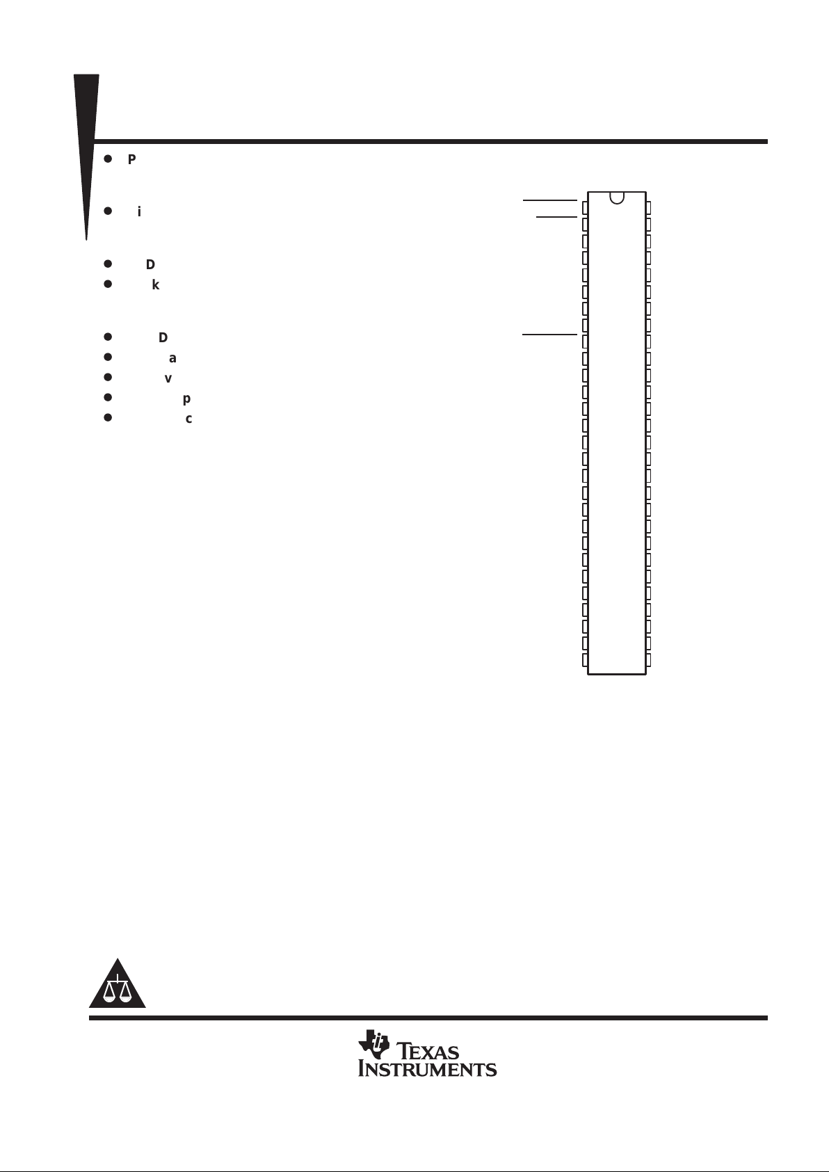
RSTFLTR
RESET
DSENS
CLK40
GND
AATN–
TEST
AACK–
TIMEOUT
AREQ–
AC/D–
V
CC
GND
GND
GND
GND
GND
V
CC
DRVBUS
SDB
AMSG–
AI/O–
ASEL–
NC
ABSY–
NC
ARST–
NC
X2
X1/CLK20
NC
BATN–
BATN+
BACK–
BACK+
BREQ–
BREQ+
BC/D–
BC/D+
V
CC
GND
GND
GND
GND
GND
V
CC
BMSG–
BMSG+
BI/O–
BI/O+
BSEL+
BSEL–
BBSY+
BBSY–
BRST+
BRST–
DGG OR DL PACKAGE
(TOP VIEW)
NC – No internal connection
Terminals 13 through 17 and 40 through 44 are
connected together to the package lead frame and
signal ground.
SN75970B
SCSI DIFFERENTIAL CONVERTER-CONTROL
SLLS323A – NOVEMBER 1999 – REVISED JANUARY 2000
2
POST OFFICE BOX 655303 • DALLAS, TEXAS 75265
description (continued)
The differential SCSI bus interface consists of
bipolar bidirectional inputs and outputs that meet
or exceed the requirements of EIA-485 and ISO
8482-1982/TIA TR30.2 referenced by the American National Standard of Information Systems
(ANSI) X3.131-1994 Small Computer System
Interface-2 (SCSI-2) and SCSI-3 Fast-20 Parallel
Interface (Fast-20) X3.277:1996.
The SN75970B is characterized for operation
over the temperature range of 0°C to 70°C.
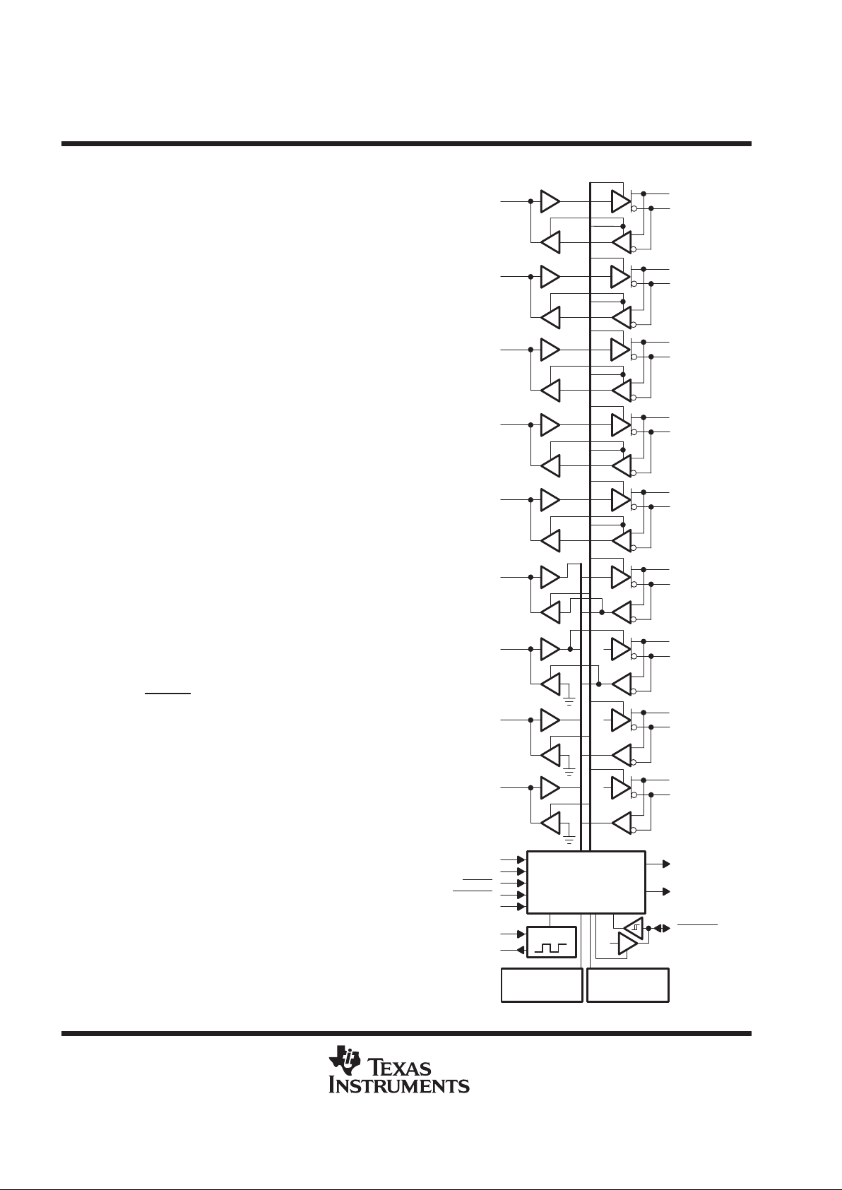
The SN75970B consists of nine RS-485 differential transceivers, nine TTL- or CMOS-level
compatible transceivers, a state machine and
control logic block, a 20-MHz crystal-controlled
oscillator, a timer, a power-up/-down glitch
protection circuit, and a thermal-shutdown
protection circuit.
The single-ended or controller interface is
designated as the A side and the differential port
is the B side. Since the device uses the SCSI
control signals to decode the state of the bus and
data flow direction, the terminal assignments must
be matched to the corresponding signal on the
SCSI bus. The signal name followed by a a minus
sign (–) indicates an active-low signal while a plus
sign (+) indicates an active-high signal.
A reset function, which disables all outputs and
clears internal latches, can be accomplished from
two external inputs and two internally generated
signals. RESET
(Reset) and DSENS (differential
sense) are available to external circuits for a bus
reset or to disable all outputs should a
single-ended cable be inadvertently connected to
a differential connector. The power-up and
thermal-shutdown are internally generated signals that have the same effect when the supply
voltage is below 3.5 V or the junction temperature
exceeds approximately 175°C.
This data sheet contains descriptions of the
SN75970B input and output signals followed by
the electrical characteristics. The parameter
measurement information is followed by the
theory of operation, a state flow chart, and a
typical circuit in the application information
section.
53
52
BATN–
BATN+
6
51
50
BACK–
BACK+
8
38
37
BMSG–
BMSG+
21
47
46
BC/D–
BC/D+
11
36
35
BI/O–
BI/O+
22
30
29
BRST+
BRST–
27
H
32
31
BBSY+
BBSY–
25
H
34
33
BSEL+
BSEL–
23
H
State Machine and
Control Logic
Oscillator
H
Thermal
Shutdown
Power-Up
and Reset Logic
3
7
2
1
4
55
56
19
DRVBUS
20
SDB
TIMEOUT
AATN–
AACK–
AMSG–
AC/D–
AI/O–
ARST–
ABSY–
ASEL–
49
48
BREQ–
BREQ+
10
AREQ–
9
DSENS
TEST
RESET
RSTFLTR
CLK40
X1/CLK20
X2
logic diagram (positive logic)
SN75970B
SCSI DIFFERENTIAL CONVERTER-CONTROL
SLLS323A – NOVEMBER 1999 – REVISED JANUARY 2000
3
POST OFFICE BOX 655303 • DALLAS, TEXAS 75265
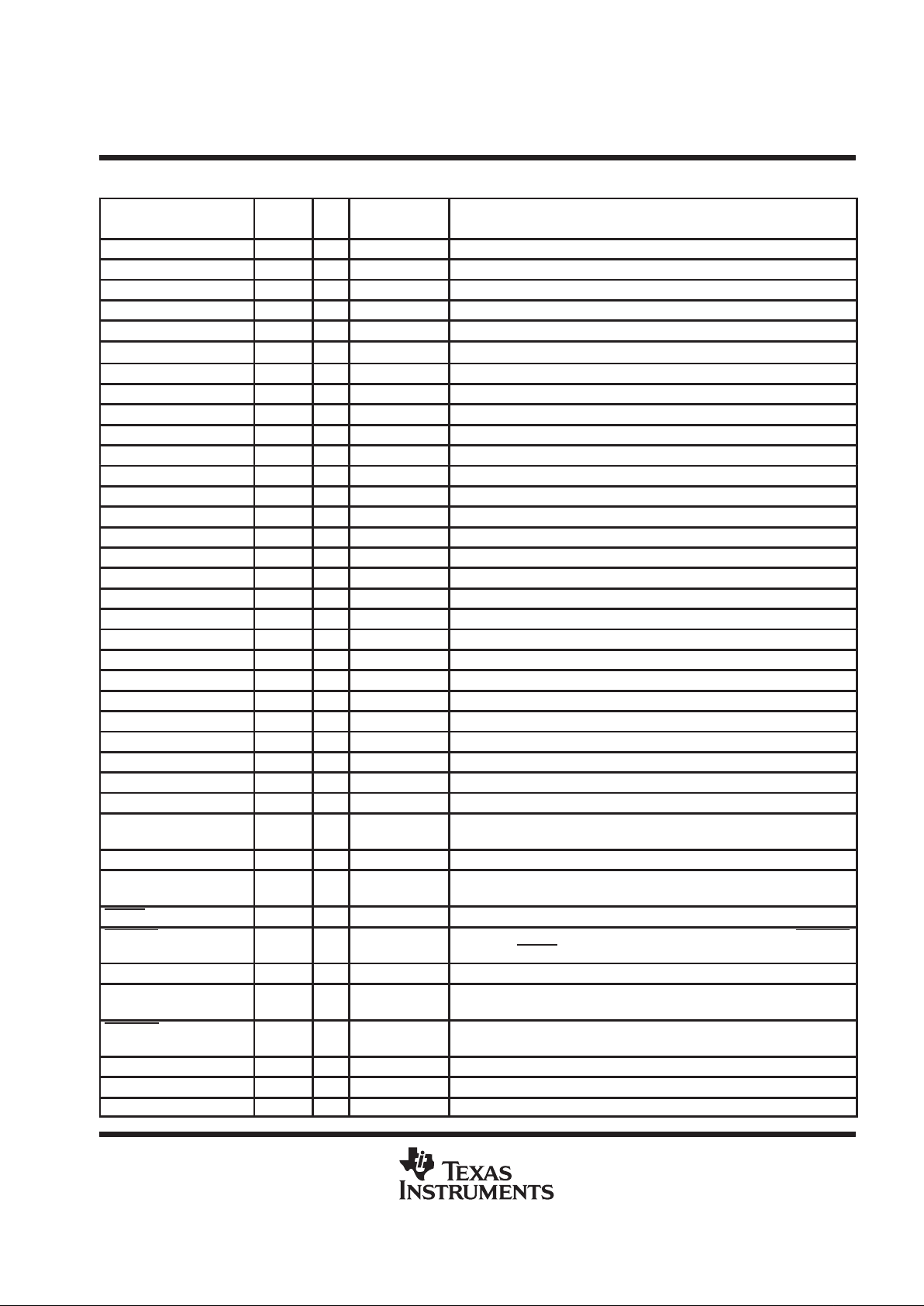
Terminal Functions
TERMINAL
LOGIC
NAME NO.
LEVEL
I/O
TERMINATION
DESCRIPTION
AACK– 8 TTL I/O strong pullup SCSI acknowledge (–ACK) signal to/from controller
AATN– 6 TTL I/O strong pullup SCSI attention (–ATN) signal to/from controller
ABSY– 25 TTL I/O strong pullup SCSI busy (–BSY) signal to/from the controller
AC/D– 11 TTL I/O strong pullup SCSI control/data (–C/D) signal to/from the controller
AI/O– 22 TTL I/O strong pullup SCSI input/output (–I/O) signal to/from the controller
AMSG– 21 TTL I/O strong pullup SCSI message (–MSG) signal to/from the controller
AREQ– 10 TTL I/O strong pullup SCSI request (–REQ) signal to/from controller
ARST– 27 TTL I/O strong pullup SCSI reset (–RST) signal to/from the controller
ASEL– 23 TTL I/O strong pullup SCSI select (–SEL) signal to/from the controller
BACK– 51 RS-485 I/O weak pullup SCSI acknowledge (–ACK) signal to/from the bus
BACK+ 50 RS-485 I/O weak pulldown SCSI acknowledge (+ACK) signal to/from the bus
BATN– 53 RS-485 I/O weak pullup SCSI attention (–ATN) signal to/from the bus
BATN+ 52 RS-485 I/O weak pulldown SCSI attention (+ATN) signal to/from the bus
BBSY– 31 RS-485 I/O weak pulldown SCSI busy (–BSY) signal to/from the bus
BBSY+ 32 RS-485 I/O weak pullup SCSI busy (+BSY) signal to/from the bus
BC/D– 47 RS-485 I/O weak pullup SCSI control/data (–C/D) signal to/from the bus
BC/D+ 46 RS-485 I/O weak pulldown SCSI control/data (+C/D) signal to/from the bus
BI/O– 36 RS-485 I/O weak pullup SCSI input/output (–I/O) signal to/from the bus
BI/O+ 35 RS-485 I/O weak pulldown SCSI input/output (+I/O) signal to/from the bus
BMSG– 38 RS-485 I/O weak pullup SCSI message (–MSG) signal to/from the bus
BMSG+ 37 RS-485 I/O weak pulldown SCSI message (+MSG) signal to/from the bus
BREQ– 49 RS-485 I/O weak pullup SCSI request (–REQ) signal to/from the bus
BREQ+ 48 RS-485 I/O weak pulldown SCSI request (+REQ) signal to/from the bus
BRST– 29 RS-485 I/O weak pulldown SCSI reset (–RST) signal to/from the bus
BRST+ 30 RS-485 I/O weak pullup SCSI reset (+RST) signal to/from the bus
BSEL– 33 RS-485 I/O weak pulldown SCSI select (–SEL) signal to/from the bus
BSEL+ 34 RS-485 I/O weak pullup SCSI select (+SEL) signal to/from the bus
CLK40 4 CMOS I strong pulldown 40-MHz clock input
DRVBUS 19 TTL O N/A Driver bus. A high-level logic signal that indicates the SCSI bus is in one of
the information transfer phases.
DSENS 3 TTL I weak pullup A low-level input initializes the internal latches and disables all drivers.
GND 5, 13–17,
40–44
N/A N/A N/A Supply common
RESET 2 TTL I weak pullup Reset. A low-level input initializes the internal latches and disables all drivers.
RSTFLTR 1 TTL I weak pullup Reset filter. Filtered input from the SCSI bus for a system reset. RSTFLTR
differs from RESET by keeping the ARST and BRST drivers enabled.
SDB 20 TTL O N/A A high-level logic signal that indicates a differential to single-ended data flow.
TEST 7 TTL I weak pulldown Test. A high-level input that places the device in a test mode (see Table 1).
It is grounded during normal operation.
TIMEOUT 9 Analog I/O N/A Time out. This signal connects to an external RC time constant for a time out
during bus arbitration.
V
CC
12, 18, 39, 45 N/A N/A N/A 5-V supply voltage
X1/CLK20 55 CMOS I none 20-MHz crystal oscillator or clock input
X2 56 Analog O none 20-MHz crystal oscillator feedback
SN75970B
SCSI DIFFERENTIAL CONVERTER-CONTROL
SLLS323A – NOVEMBER 1999 – REVISED JANUARY 2000
4
POST OFFICE BOX 655303 • DALLAS, TEXAS 75265
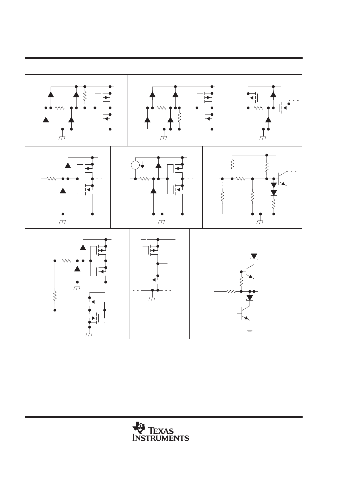
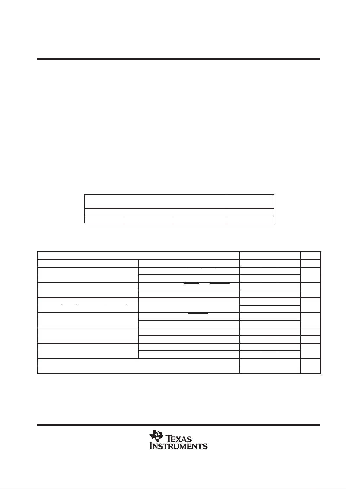
schematics of inputs and outputs
22 k
200 Ω
Input
V
CC
RSTFLTR
, RESET, AND DSENS
50 kΩ
200 Ω
Input
V
CC
TEST
200 Ω
Input
V
CC
TIMEOUT
200 Ω
Input
V
CC
CLK40
200 Ω
Input
V
CC
A
3 kΩ
12 kΩ
1 kΩ
100 kΩ
B– Pin Only
100 kΩ
B+ Pin Only
18 kΩ
V
CC
Input
B+ AND B– Inputs
200 Ω
100 kΩ
X1/CLK20
V
CC
V
CC
X2
X1/CLK20, X2
V
CC
Output
A, SDB, DRVBUS
4 mA
V
CC
Output
B+ AND B– Outputs
18 kΩ
B–
B+
SN75970B
SCSI DIFFERENTIAL CONVERTER-CONTROL
SLLS323A – NOVEMBER 1999 – REVISED JANUARY 2000
5
POST OFFICE BOX 655303 • DALLAS, TEXAS 75265
absolute maximum ratings over operating free-air temperature range (unless otherwise noted)
†
Supply voltage range, V
CC
(see Note 1) –0.3 V to 6 V. . . . . . . . . . . . . . . . . . . . . . . . . . . . . . . . . . . . . . . . . . . . . .
Differential bus voltage range (B side) –10 V to 15 V. . . . . . . . . . . . . . . . . . . . . . . . . . . . . . . . . . . . . . . . . . . . . . . .
Signal-ended bus voltage range (A side and control) –0.3 V to 7 V. . . . . . . . . . . . . . . . . . . . . . . . . . . . . . . . . . .
Continuous total power dissipation See Dissipation Rating Table. . . . . . . . . . . . . . . . . . . . . . . . . . . . . . . . . . . . .
Electrostatic discharge: B side (see Note 2):Class 3, A: 12 kV. . . . . . . . . . . . . . . . . . . . . . . . . . . . . . . . . . . . . . .
Class 3, B: 400 V. . . . . . . . . . . . . . . . . . . . . . . . . . . . . . . . . . . . . . .
All terminals: Class 2, A: 4 kV. . . . . . . . . . . . . . . . . . . . . . . . . . . . . . . . . . . . . . . . . . . . . .
Class 2, B: 400 V. . . . . . . . . . . . . . . . . . . . . . . . . . . . . . . . . . . . . . . . . . . . .
Operating free-air temperature range, T
A
0°C to 70°C. . . . . . . . . . . . . . . . . . . . . . . . . . . . . . . . . . . . . . . . . . . . . .
Storage temperature range, T
stg
–65°C to 150°C. . . . . . . . . . . . . . . . . . . . . . . . . . . . . . . . . . . . . . . . . . . . . . . . . . .
Lead temperature 1,6 mm (1/16 inch) from case for 10 seconds 260°C. . . . . . . . . . . . . . . . . . . . . . . . . . . . . . .
†
Stresses beyond those listed under “absolute maximum ratings” may cause permanent damage to the device. These are stress ratings only, and
functional operation of the device at these or any other conditions beyond those indicated under “recommended operating conditions” is not
implied. Exposure to absolute-maximum-rated conditions for extended periods may affect device reliability.
NOTES: 1. All voltage values are with respect to the GND terminals.
2. This absolute maximum rating is tested in accordance with MIL-STD-883C, Method 3015.7.
DISSIPATION RATING TABLE
PACKAGE
TA ≤ 25°C
POWER RATING
OPERATING FACTOR
‡
ABOVE TA = 25°C
TA = 70°C
POWER RATING
DGG 3333 mW 26.7 mW/°C 2133 mW
DL 3709 mW 29.7 mW/°C 2374 mW
‡
This is the inverse of the traditional junction-to-case thermal resistance (R
θJA
) for High-K (per
JEDEC) PCB installations.
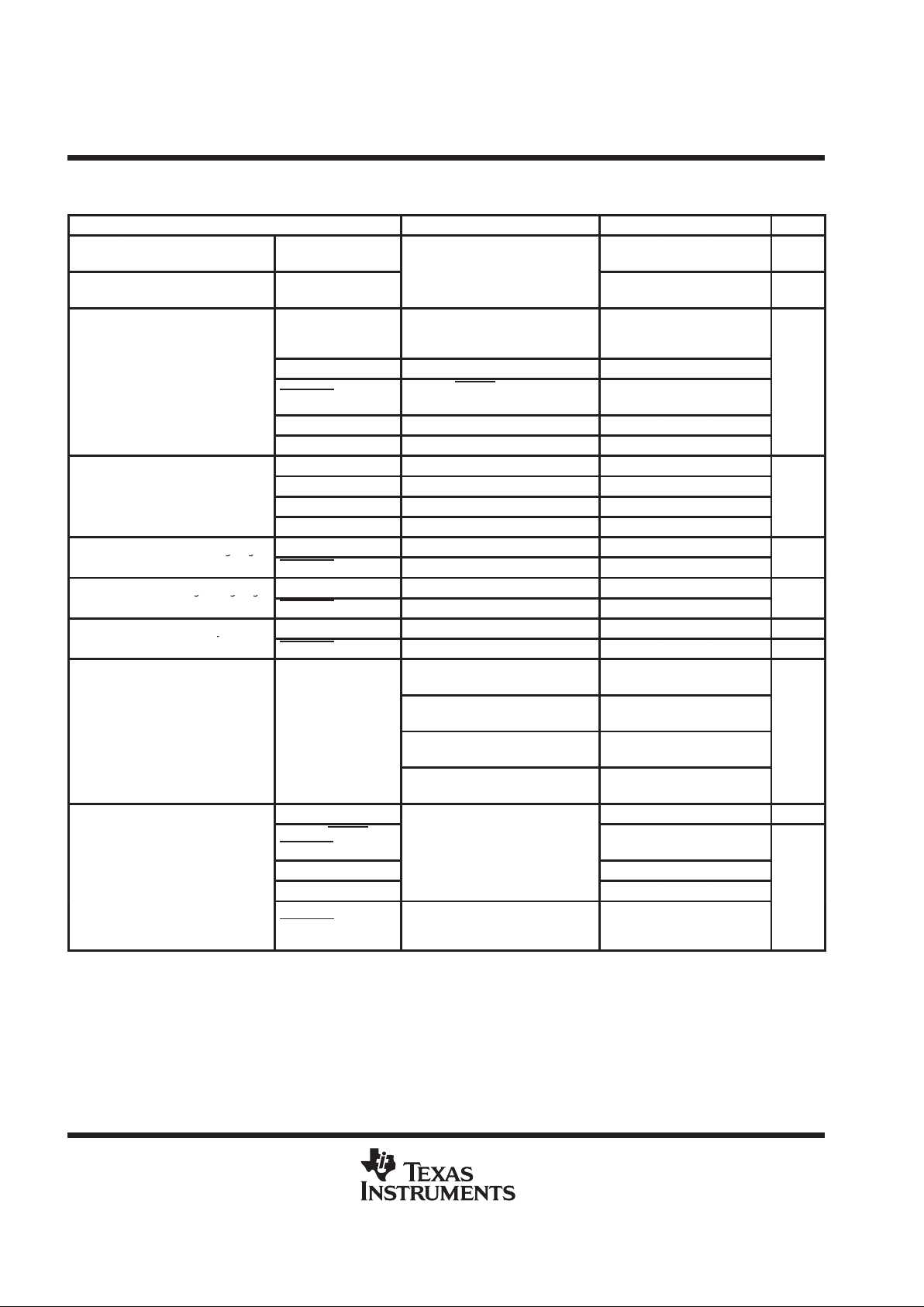
recommended operating conditions
MIN NOM MAX UNIT
Supply voltage, V
CC
4.75 5 5.25 V
p
A side, DSENS, TEST, RESET, AND RSTFLTR 2
High-level input voltage, V
IH
CLK40 AND X1/CLK20 0.7 V
CC
V
p
A side, DENS, TEST, RESET, and RSTFLTR 0.8
Low-level input voltage, V
IL
CLK40 AND X1/CLK20 0.2 V
CC
V
Input voltage at any bus terminal (separately or
12
gy ( y
common-mode), V
I
B side–7V
p
A side, DRVBUS, SDB, TIMEOUT –16
High-level output current, I
OH
X2 –4
mA
p
A side, DRVBUS, and SDB 16 mA
Low-level output current, I
OL
X2 4 mA
CLK20 20
Clock frequenc
y,
f
CLK
CLK40 40
MH
z
Operating case temperature, T
C
0 125 °C
Operating free-air temperature, T
A
0 70 °C
SN75970B
SCSI DIFFERENTIAL CONVERTER-CONTROL
SLLS323A – NOVEMBER 1999 – REVISED JANUARY 2000
6
POST OFFICE BOX 655303 • DALLAS, TEXAS 75265
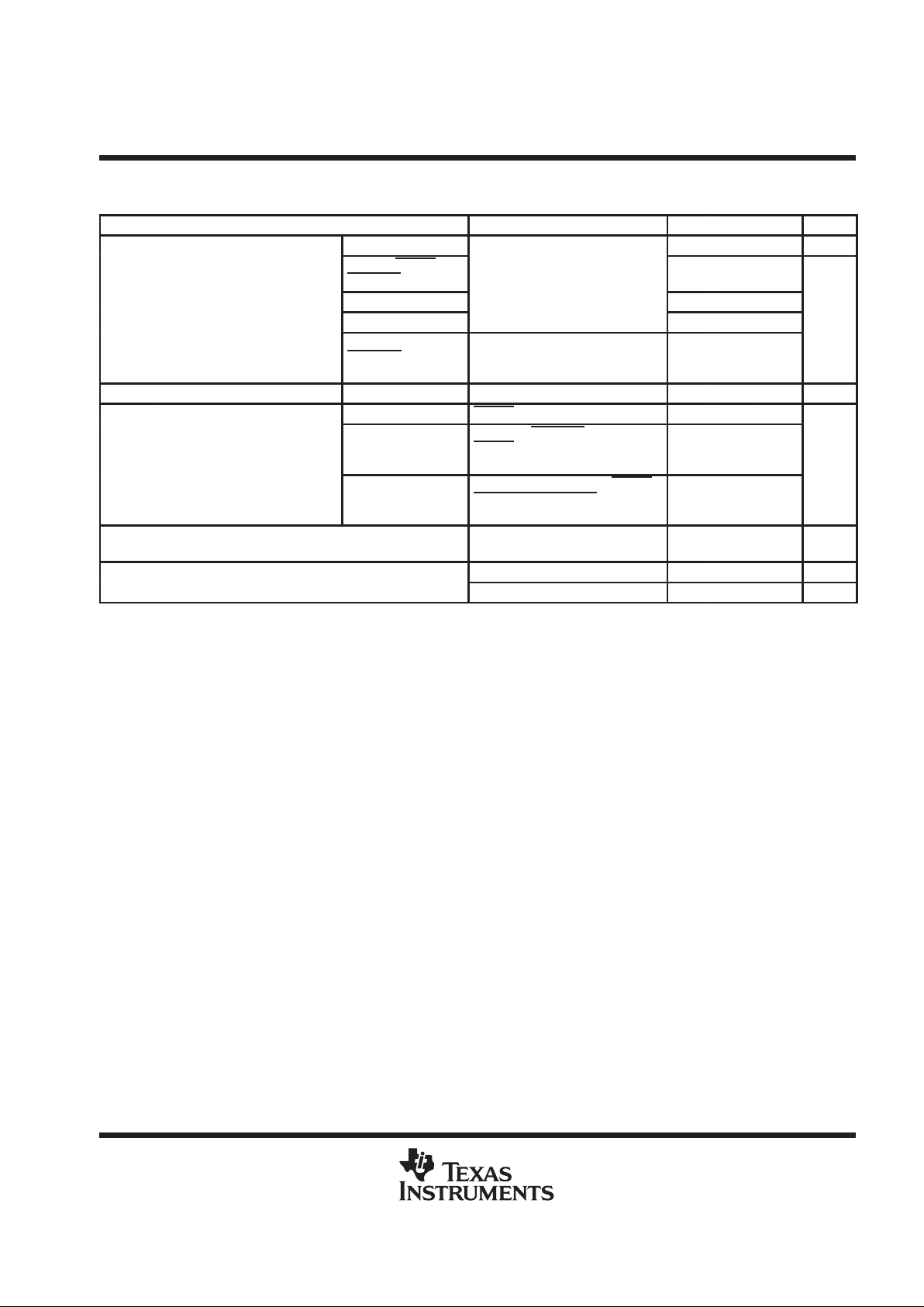
electrical characteristics over recommended operating free-air temperature range (unless
otherwise noted)
PARAMETER TEST CONDITIONS MIN TYP
†
MAX UNIT
V
OD(H)
Driver differential
high-level output voltage
B side except BBSY,
BRST, and BSEL
–0.8 –2.2 V
V
OD(L)
Driver differential
low-level output voltage
B side
See Figure 1
1 1.8 V
AACK–, AATN–,
AC/D–, AI/O–,
AMSG–, AREQ–
VID = –200 V, IOH = –16 mA 2.5 4.3
DRVBUS, SDB IOH = –16 mA 2.5 4.4
V
OH
High-level output voltage
TIMEOUT
Test and RESET at 0.8 V,
All others open, IOH = –16 mA
2.5 4.5
V
B side 3.4
X2 IOH = - 4 mA 3.2
DRVBUS, SDB IOL = 16 mA 0.8
p
A side VID = 200 mV, IOL = 16 mA 0.8
VOLLow-level output voltage
B side 1.6
V
X2 IOL = 4 mA 0.8
Receiver positive-going
B side IOH = –16 mA, See Figure 2 0.2
V
IT+
gg
input threshold voltage
TIMEOUT
2.6
V
Receiver negative-going
B side IOL = 16 mA, See Figure 2 –0.2
‡
V
IT–
ggg
input threshold voltage
TIMEOUT
0.32V
CC
0.4 V
CC
V
Receiver input hysteresis
B side 45 mV
V
hys
y
(V
IT+
– V
IT–
)
TIMEOUT
0.5 V
VI = 12 V, VCC = 5 V,
All other inputs at 0 V
0.6 1
p
VI = 12 V, VCC = 0,
All other inputs at 0 V
0.7 1
IIBus input current
B side
VI = –7 V, VCC = 5 V,
All other inputs at 0 V
–0.5 –0.8
mA
VI = –7 V, VCC = 0,
All other inputs at 0 V
–0.4 –0.8
A side –2.0 –6 –8 mA
DSENS, RESET,
RSTFLTR
V
= 2 V
–60 –100
-
p
CLK40, X1/CLK20
IH
±20
IIHHigh-level in ut current
TEST 100
µA
TIMEOUT
TEST at 2 V, A side and other
control inputs at 0.8 V ,
B side open, VIH = 2 V
±25
†
All typical values are at VCC = 5 V, TA = 25°C.
‡
The algebraic convention with the least positive (more negative) limit is designated minimum, is used in this data sheet for the differential input
voltage only.
SN75970B
SCSI DIFFERENTIAL CONVERTER-CONTROL
SLLS323A – NOVEMBER 1999 – REVISED JANUARY 2000
7
POST OFFICE BOX 655303 • DALLAS, TEXAS 75265
electrical characteristics over recommended operating free-air temperature range (unless
otherwise noted) (Continued)
PARAMETER TEST CONDITIONS MIN TYP†MAX UNIT
A side –6 –9 mA
DSENS, RESET,
RSTFLTR
V
= 0.8 V
–100
-
p
CLK40, X1/CLK20
IL
±30
IILLow-level in ut current
TEST ±30
µA
TIMEOUT
TEST at 2 V, A side and other
control inputs at 0.8 V ,
B side open, VIL = 0.8 V
±25
I
OS
Short circuit output current B side VO = 5 V and 0 V ±250 mA
Disabled RESET at 0.8 V, All others open 32 42
I
CC
Supply current
All A-side to B-side
channels enabled
TEST and RSTFLTR at 2 V
RESET
at 0.8 V,
All other inputs open, No load
72 95
mA
All B-side to A-side
channels enabled
TEST and B+ pins at 2 V , RESET,
RSTFLTR, and B– pins
at 0.8 V,
All other inputs open, No load
51 72
C
o
Bus output capacitance
B side to GND,
VI = 0.6 sin(2π 106 t)+ 1.5 V
18 21 pF
p
p
B side to A side, one channel 40 pF
CpdPower dissipation capacitance (see Note 3)
A side to B side, one channel 100 pF
†
All typical values are at VCC = 5 V, TA = 25°C.
NOTE 3: Cpd determines the no-load dynamic current consumption, IS = Cpd × VCC × f + ICC (ICC depends upon the output states and load circuits
and is not necessarily the same ICC as specified in the electrical tables).
 Loading...