

Page 1
SN75970B
SCSI DIFFERENTIAL CONVERTER-CONTROL
SLLS323A – NOVEMBER 1999 – REVISED JANUARY 2000
D
Provides High-Voltage Differential SCSI
from Single-Ended Controller When Used
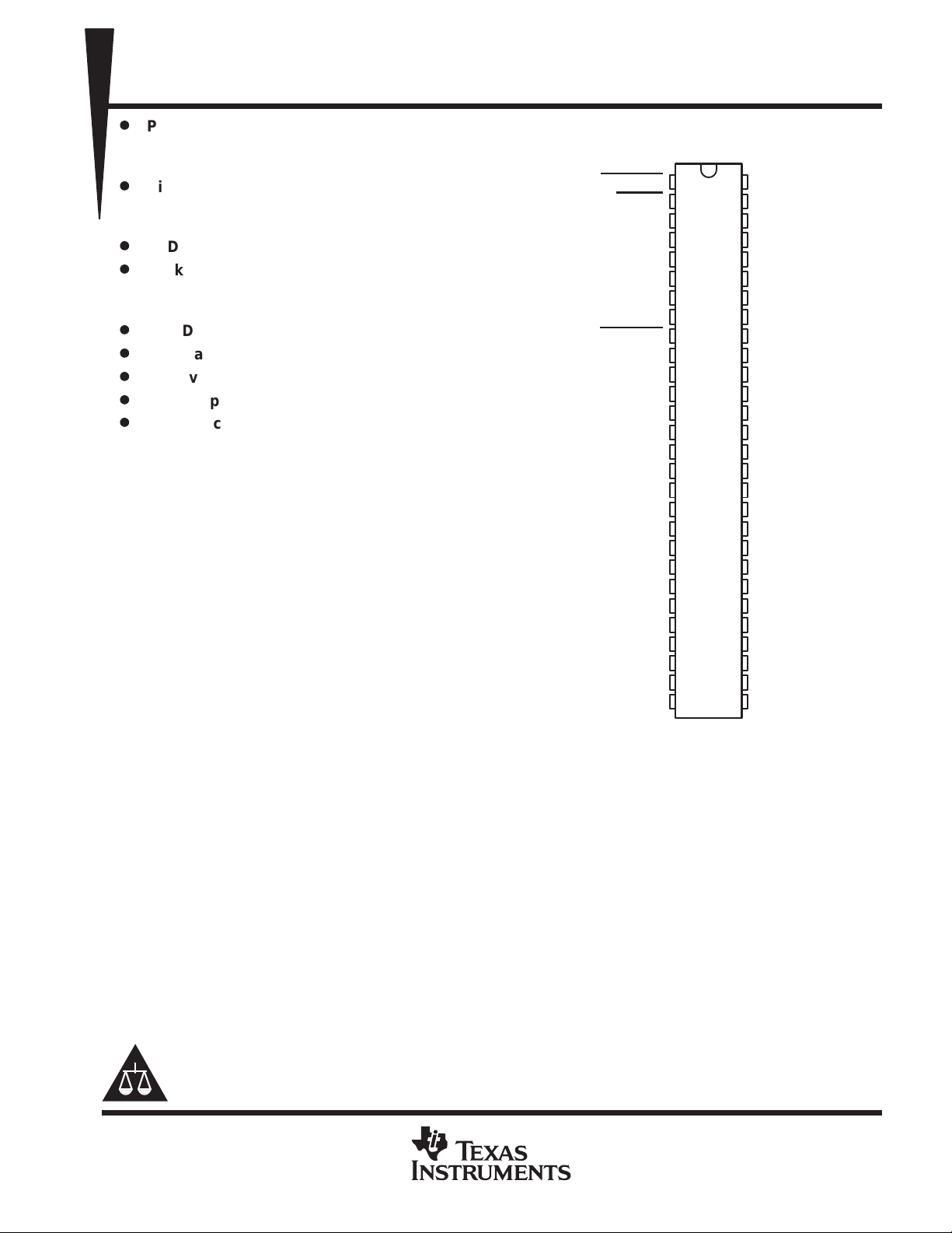
DGG OR DL PACKAGE
(TOP VIEW)
With the SN75971B Data Transceiver
D
Nine Transceivers Meet or Exceed the
Requirements of ANSI Standard EIA-485
and ISO-8482 Standards
D
ESD Protection on Bus Pins to 12 kV
D
Packaged in Shrink Small-Outline Package
with 25 mil Terminal Pitch and Thin
Small-Package with 20 mil Terminal Pitch
D
Low Disabled Supply Current 32 mA Typ
D
Thermal Shutdown Protection
D
Positive- and Negative-Current Limiting
D
Power-Up/-Down Glitch Protection
D
Open-Circuit Failsafe Receivers
description
The SN75970B SCSI differential convertercontrol, when used in conjunction with one or
more of its companion data transceiver(s),
provides the superior electrical performance of
differential SCSI from a single-ended SCSI bus
controller. A 16-bit, Fast-SCSI bus can be
implemented with just three devices (two for data
and one for control) in the space-efficient, 56-pin,
shrink small-outline package (SSOP) as well as
the even smaller TSSOP and a few external
components.
The SN75970B is available in a B2 (20 Mxfer)
RSTFLTR
RESET
DSENS
CLK40
GND
AATN–
TEST
AACK–
TIMEOUT
AREQ–
AC/D–
V
CC
GND
GND
GND
GND
GND
V
CC
DRVBUS
SDB
AMSG–
AI/O–
ASEL–
NC
ABSY–
NC
ARST–
NC
1
2
3
4
5
6
7
8
9
10
11
12
13
14
15
16
17
18
19
20
21
22
23
24
25
26
27
28
56
55
54
53
52
51
50
49
48
47
46
45
44
43
42
41
40
39
38
37
36
35
34
33
32
31
30
29
X2
X1/CLK20
NC
BATN–
BATN+
BACK–
BACK+
BREQ–
BREQ+
BC/D–
BC/D+
V
CC
GND
GND
GND
GND
GND
V
CC
BMSG–
BMSG+
BI/O–
BI/O+
BSEL+
BSEL–
BBSY+
BBSY–
BRST+
BRST–
version and a B1 (10 Mxfer) version.
NC – No internal connection
In a typical differential SCSI node, the SCSI
controller provides the enables for each external
Terminals 13 through 17 and 40 through 44 are
connected together to the package lead frame and
signal ground.
RS-485 transceiver. This could require as many
as 27 additional terminals for a 16-bit differential bus controller or relegate a 16-bit single-ended controller to
only an 8-bit differential bus. Using the standard nine SCSI control signals, the SN75970B control transceiver
decodes the state of the bus and enables the SN75971B data transceiver(s) to transmit the single-ended SCSI
input signals differentially to the cable or receive the differential cable signals and drive the single-ended outputs
to the controller.
The single-ended SCSI bus interface consists of CMOS bidirectional inputs and outputs. The drivers are rated
at ±16 mA of output current. The receiver inputs are pulled high with approximately 4 mA to eliminate the need
for external pullup resistors for the open-drain outputs of most single-ended SCSI controllers. The single-ended
side of the device is not intended to drive the SCSI bus directly.
Please be aware that an important notice concerning availability, standard warranty, and use in critical applications of
Texas Instruments semiconductor products and disclaimers thereto appears at the end of this data sheet.
PRODUCTION DATA information is current as of publication date.
Products conform to specifications per the terms of Texas Instruments
standard warranty. Production processing does not necessarily include
testing of all parameters.
POST OFFICE BOX 655303 • DALLAS, TEXAS 75265
Copyright 2000, Texas Instruments Incorporated
1
Page 2

SN75970B
SCSI DIFFERENTIAL CONVERTER-CONTROL
SLLS323A – NOVEMBER 1999 – REVISED JANUARY 2000
description (continued)
The differential SCSI bus interface consists of
bipolar bidirectional inputs and outputs that meet
or exceed the requirements of EIA-485 and ISO
8482-1982/TIA TR30.2 referenced by the American National Standard of Information Systems
(ANSI) X3.131-1994 Small Computer System
Interface-2 (SCSI-2) and SCSI-3 Fast-20 Parallel
Interface (Fast-20) X3.277:1996.
The SN75970B is characterized for operation
over the temperature range of 0°C to 70°C.
The SN75970B consists of nine RS-485 differential transceivers, nine TTL- or CMOS-level
compatible transceivers, a state machine and
control logic block, a 20-MHz crystal-controlled
oscillator, a timer, a power-up/-down glitch
protection circuit, and a thermal-shutdown
protection circuit.
The single-ended or controller interface is
designated as the A side and the differential port
is the B side. Since the device uses the SCSI
control signals to decode the state of the bus and
data flow direction, the terminal assignments must
be matched to the corresponding signal on the
SCSI bus. The signal name followed by a a minus
sign (–) indicates an active-low signal while a plus
sign (+) indicates an active-high signal.
A reset function, which disables all outputs and
clears internal latches, can be accomplished from
two external inputs and two internally generated
signals. RESET
sense) are available to external circuits for a bus
reset or to disable all outputs should a
single-ended cable be inadvertently connected to
a differential connector. The power-up and
thermal-shutdown are internally generated signals that have the same effect when the supply
voltage is below 3.5 V or the junction temperature
exceeds approximately 175°C.
This data sheet contains descriptions of the
SN75970B input and output signals followed by
the electrical characteristics. The parameter
measurement information is followed by the
theory of operation, a state flow chart, and a
typical circuit in the application information
section.
(Reset) and DSENS (differential
logic diagram (positive logic)
AC/D–
AI/O–
TEST
CLK40
6
8
21
11
10
22
27
25
23
3
7
2
1
4
55
56
X2
State Machine and
Control Logic
Oscillator
Power-Up
and Reset Logic
H
H
H
H
Shutdown
AATN–
AACK–
AMSG–
AREQ–
ARST–
ABSY–
ASEL–
DSENS
RESET
RSTFLTR
X1/CLK20
Thermal
53
52
51
50
38
37
47
46
49
48
36
35
30
29
32
31
34
33
19
20
9
BATN–
BATN+
BACK–
BACK+
BMSG–
BMSG+
BC/D–
BC/D+
BREQ–
BREQ+
BI/O–
BI/O+
BRST+
BRST–
BBSY+
BBSY–
BSEL+
BSEL–
DRVBUS
SDB
TIMEOUT
2
POST OFFICE BOX 655303 • DALLAS, TEXAS 75265
Page 3
SCSI DIFFERENTIAL CONVERTER-CONTROL
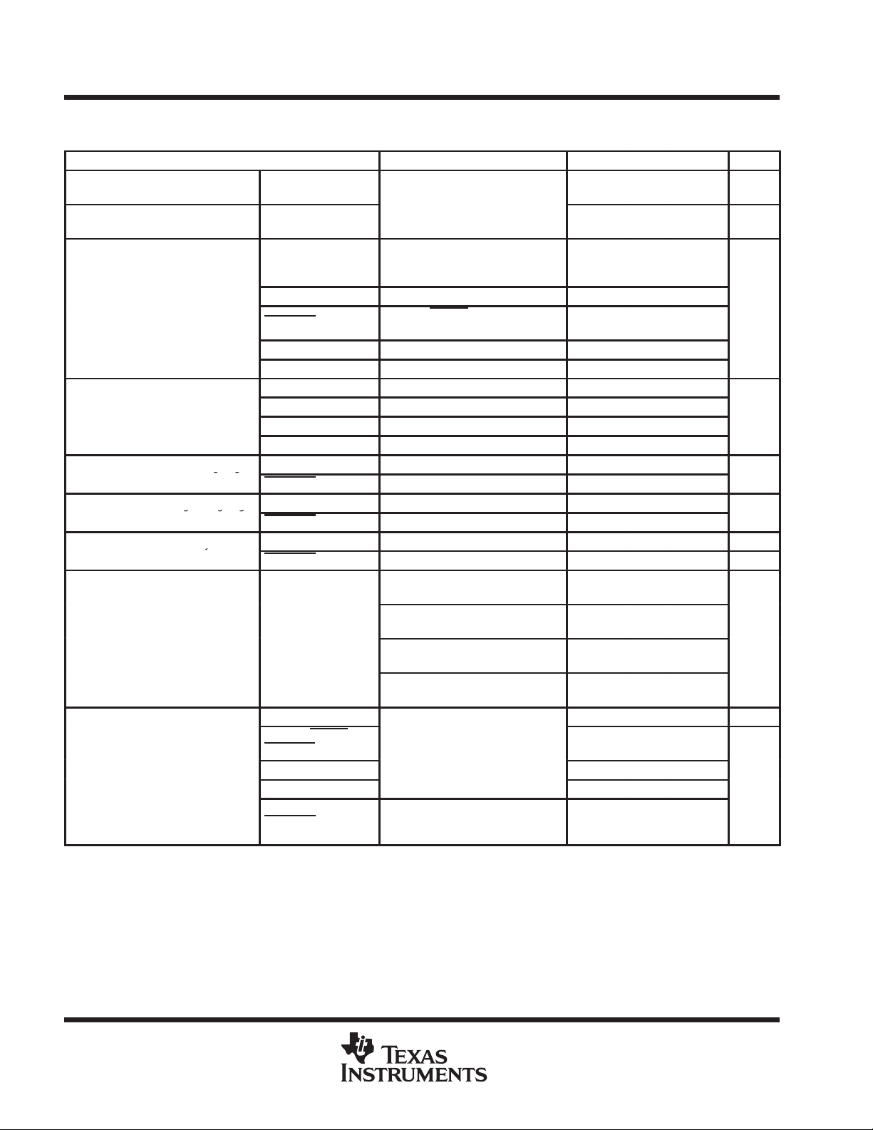
I/O
TERMINATION
DESCRIPTION
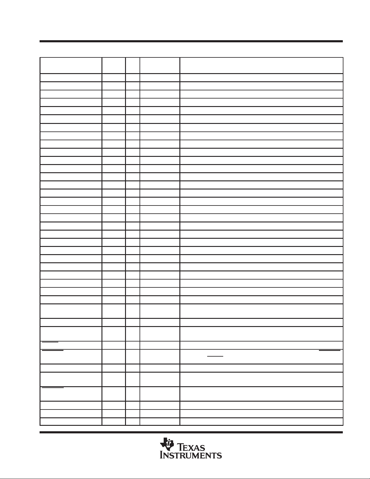
Terminal Functions
SN75970B
SLLS323A – NOVEMBER 1999 – REVISED JANUARY 2000
TERMINAL
NAME NO.
AACK– 8 TTL I/O strong pullup SCSI acknowledge (–ACK) signal to/from controller
AATN– 6 TTL I/O strong pullup SCSI attention (–ATN) signal to/from controller
ABSY– 25 TTL I/O strong pullup SCSI busy (–BSY) signal to/from the controller
AC/D– 11 TTL I/O strong pullup SCSI control/data (–C/D) signal to/from the controller
AI/O– 22 TTL I/O strong pullup SCSI input/output (–I/O) signal to/from the controller
AMSG– 21 TTL I/O strong pullup SCSI message (–MSG) signal to/from the controller
AREQ– 10 TTL I/O strong pullup SCSI request (–REQ) signal to/from controller
ARST– 27 TTL I/O strong pullup SCSI reset (–RST) signal to/from the controller
ASEL– 23 TTL I/O strong pullup SCSI select (–SEL) signal to/from the controller
BACK– 51 RS-485 I/O weak pullup SCSI acknowledge (–ACK) signal to/from the bus
BACK+ 50 RS-485 I/O weak pulldown SCSI acknowledge (+ACK) signal to/from the bus
BATN– 53 RS-485 I/O weak pullup SCSI attention (–ATN) signal to/from the bus
BATN+ 52 RS-485 I/O weak pulldown SCSI attention (+ATN) signal to/from the bus
BBSY– 31 RS-485 I/O weak pulldown SCSI busy (–BSY) signal to/from the bus
BBSY+ 32 RS-485 I/O weak pullup SCSI busy (+BSY) signal to/from the bus
BC/D– 47 RS-485 I/O weak pullup SCSI control/data (–C/D) signal to/from the bus
BC/D+ 46 RS-485 I/O weak pulldown SCSI control/data (+C/D) signal to/from the bus
BI/O– 36 RS-485 I/O weak pullup SCSI input/output (–I/O) signal to/from the bus
BI/O+ 35 RS-485 I/O weak pulldown SCSI input/output (+I/O) signal to/from the bus
BMSG– 38 RS-485 I/O weak pullup SCSI message (–MSG) signal to/from the bus
BMSG+ 37 RS-485 I/O weak pulldown SCSI message (+MSG) signal to/from the bus
BREQ– 49 RS-485 I/O weak pullup SCSI request (–REQ) signal to/from the bus
BREQ+ 48 RS-485 I/O weak pulldown SCSI request (+REQ) signal to/from the bus
BRST– 29 RS-485 I/O weak pulldown SCSI reset (–RST) signal to/from the bus
BRST+ 30 RS-485 I/O weak pullup SCSI reset (+RST) signal to/from the bus
BSEL– 33 RS-485 I/O weak pulldown SCSI select (–SEL) signal to/from the bus
BSEL+ 34 RS-485 I/O weak pullup SCSI select (+SEL) signal to/from the bus
CLK40 4 CMOS I strong pulldown 40-MHz clock input
DRVBUS 19 TTL O N/A Driver bus. A high-level logic signal that indicates the SCSI bus is in one of
DSENS 3 TTL I weak pullup A low-level input initializes the internal latches and disables all drivers.
GND 5, 13–17,
RESET 2 TTL I weak pullup Reset. A low-level input initializes the internal latches and disables all drivers.
RSTFLTR 1 TTL I weak pullup Reset filter. Filtered input from the SCSI bus for a system reset. RSTFLTR
SDB 20 TTL O N/A A high-level logic signal that indicates a differential to single-ended data flow.
TEST 7 TTL I weak pulldown Test. A high-level input that places the device in a test mode (see Table 1).
TIMEOUT 9 Analog I/O N/A Time out. This signal connects to an external RC time constant for a time out
V
CC
X1/CLK20 55 CMOS I none 20-MHz crystal oscillator or clock input
X2 56 Analog O none 20-MHz crystal oscillator feedback
40–44
12, 18, 39, 45 N/A N/A N/A 5-V supply voltage
LOGIC
LEVEL
the information transfer phases.
N/A N/A N/A Supply common
differs from RESET by keeping the ARST and BRST drivers enabled.
It is grounded during normal operation.
during bus arbitration.
POST OFFICE BOX 655303 • DALLAS, TEXAS 75265
3
Page 4
SN75970B
SCSI DIFFERENTIAL CONVERTER-CONTROL
SLLS323A – NOVEMBER 1999 – REVISED JANUARY 2000
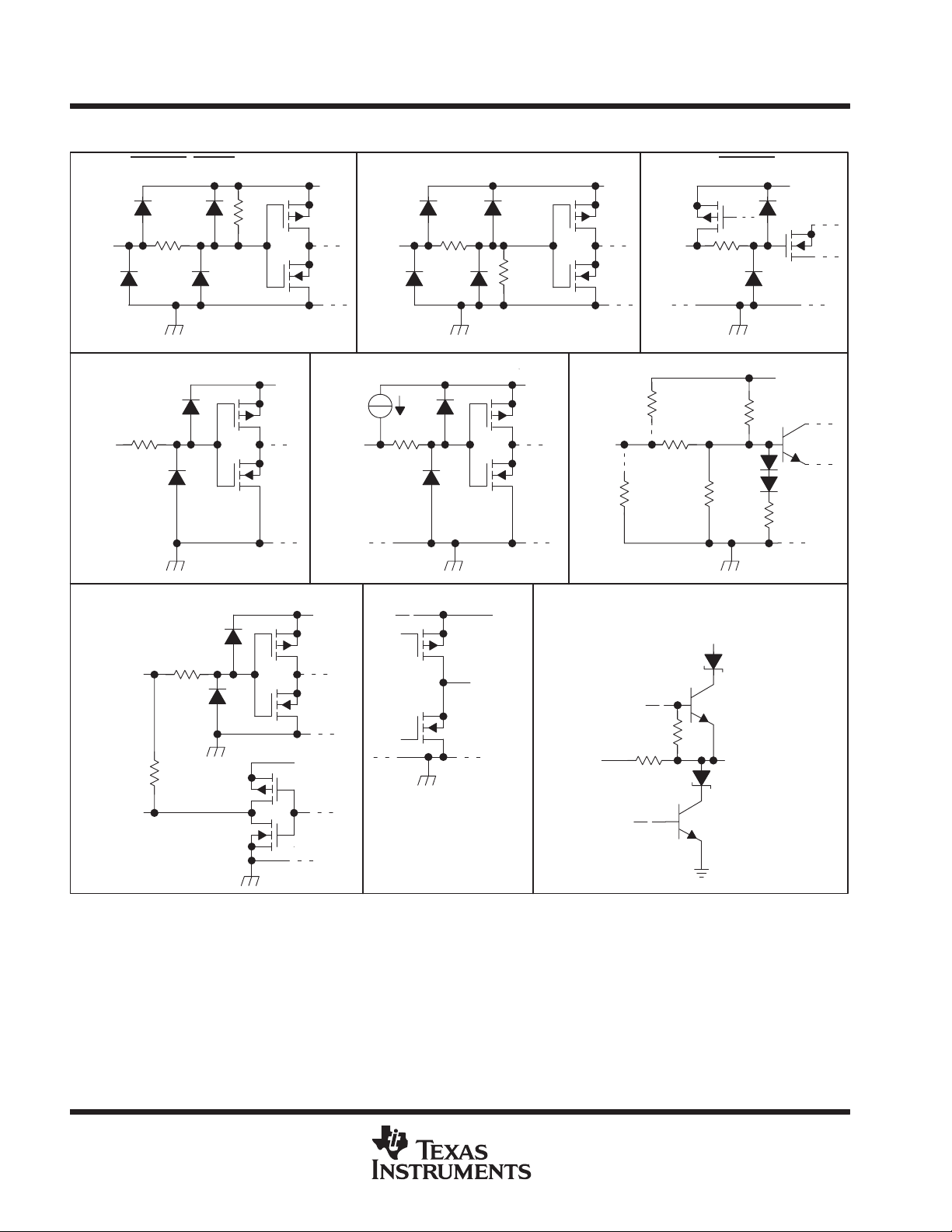
schematics of inputs and outputs
Input
Input
RSTFLTR
200 Ω
200 Ω
, RESET, AND DSENS
22 k
CLK40
V
X1/CLK20, X2
CC
V
Input
V
CC
CC
4 mA
Input
200 Ω
A, SDB, DRVBUS
200 Ω
A
TEST
V
50 kΩ
CC
TIMEOUT
V
CC
Input
B+ AND B– Inputs
V
CC
100 kΩ
B– Pin Only
Input
18 kΩ
100 kΩ
B+ Pin Only
B+ AND B– Outputs
200 Ω
12 kΩ
V
CC
3 kΩ
V
1 kΩ
CC
V
CC
X1/CLK20
X2
200 Ω
100 kΩ
Output
B–
V
CC
18 kΩ
B+
Output
4
POST OFFICE BOX 655303 • DALLAS, TEXAS 75265
Page 5
SN75970B
High-level input voltage, V
V
Low-level input voltage, V
V
gy ( y
B side–7V
High-level output current, I
mA
Low-level output current, I
Clock frequenc
f
MH
SCSI DIFFERENTIAL CONVERTER-CONTROL
SLLS323A – NOVEMBER 1999 – REVISED JANUARY 2000
absolute maximum ratings over operating free-air temperature range (unless otherwise noted)
Supply voltage range, V
Differential bus voltage range (B side) –10 V to 15 V. . . . . . . . . . . . . . . . . . . . . . . . . . . . . . . . . . . . . . . . . . . . . . . .
Signal-ended bus voltage range (A side and control) –0.3 V to 7 V. . . . . . . . . . . . . . . . . . . . . . . . . . . . . . . . . . .
Continuous total power dissipation See Dissipation Rating Table. . . . . . . . . . . . . . . . . . . . . . . . . . . . . . . . . . . . .
Electrostatic discharge: B side (see Note 2):Class 3, A: 12 kV. . . . . . . . . . . . . . . . . . . . . . . . . . . . . . . . . . . . . . .
Operating free-air temperature range, T
Storage temperature range, T
Lead temperature 1,6 mm (1/16 inch) from case for 10 seconds 260°C. . . . . . . . . . . . . . . . . . . . . . . . . . . . . . .
†
Stresses beyond those listed under “absolute maximum ratings” may cause permanent damage to the device. These are stress ratings only, and
functional operation of the device at these or any other conditions beyond those indicated under “recommended operating conditions” is not
implied. Exposure to absolute-maximum-rated conditions for extended periods may affect device reliability.
NOTES: 1. All voltage values are with respect to the GND terminals.
2. This absolute maximum rating is tested in accordance with MIL-STD-883C, Method 3015.7.
PACKAGE
DGG 3333 mW 26.7 mW/°C 2133 mW
‡
This is the inverse of the traditional junction-to-case thermal resistance (R
JEDEC) PCB installations.
(see Note 1) –0.3 V to 6 V. . . . . . . . . . . . . . . . . . . . . . . . . . . . . . . . . . . . . . . . . . . . . .
CC
Class 3, B: 400 V. . . . . . . . . . . . . . . . . . . . . . . . . . . . . . . . . . . . . . .
All terminals: Class 2, A: 4 kV. . . . . . . . . . . . . . . . . . . . . . . . . . . . . . . . . . . . . . . . . . . . . .
Class 2, B: 400 V. . . . . . . . . . . . . . . . . . . . . . . . . . . . . . . . . . . . . . . . . . . . .
0°C to 70°C. . . . . . . . . . . . . . . . . . . . . . . . . . . . . . . . . . . . . . . . . . . . . .
–65°C to 150°C. . . . . . . . . . . . . . . . . . . . . . . . . . . . . . . . . . . . . . . . . . . . . . . . . . .
stg
POWER RATING
DL 3709 mW 29.7 mW/°C 2374 mW
A
DISSIPATION RATING TABLE
TA ≤ 25°C
OPERATING FACTOR
ABOVE TA = 25°C
‡
TA = 70°C
POWER RATING
θJA
) for High-K (per
†
recommended operating conditions
Supply voltage, V
Input voltage at any bus terminal (separately or
common-mode), V
Operating case temperature, T
Operating free-air temperature, T
CC
p
p
p
p
y,
IH
IL
I
OH
OL
CLK
C
A
MIN NOM MAX UNIT
4.75 5 5.25 V
A side, DSENS, TEST, RESET, AND RSTFLTR 2
CLK40 AND X1/CLK20 0.7 V
A side, DENS, TEST, RESET, and RSTFLTR 0.8
CLK40 AND X1/CLK20 0.2 V
A side, DRVBUS, SDB, TIMEOUT –16
X2 –4
A side, DRVBUS, and SDB 16 mA
X2 4 mA
CLK20 20
CLK40 40
CC
CC
12
0 125 °C
0 70 °C
z
POST OFFICE BOX 655303 • DALLAS, TEXAS 75265
5
Page 6
SN75970B
See Figure 1
VOLLow-level output voltage
V
V
gg
V
V
ggg
V
V
y
IIBus input current
B side
mA
IH
IIHHigh-level in ut current
SCSI DIFFERENTIAL CONVERTER-CONTROL
SLLS323A – NOVEMBER 1999 – REVISED JANUARY 2000
electrical characteristics over recommended operating free-air temperature range (unless
otherwise noted)
PARAMETER TEST CONDITIONS MIN TYP
V
OD(H)
V
OD(L)
V
OH
IT+
IT–
hys
†
All typical values are at VCC = 5 V, TA = 25°C.
‡
The algebraic convention with the least positive (more negative) limit is designated minimum, is used in this data sheet for the differential input
voltage only .
Driver differential
high-level output voltage
Driver differential
low-level output voltage
High-level output voltage
p
Receiver positive-going
input threshold voltage
Receiver negative-going
input threshold voltage
Receiver input hysteresis
(V
– V
IT+
-
)
IT–
p
p
B side except BBSY,
BRST, and BSEL
B side
AACK–, AA TN–,
AC/D–, AI/O–,
AMSG–, AREQ–
DRVBUS, SDB IOH = –16 mA 2.5 4.4
TIMEOUT
B side 3.4
X2 IOH = - 4 mA 3.2
DRVBUS, SDB IOL = 16 mA 0.8
A side VID = 200 mV, IOL = 16 mA 0.8
B side 1.6
X2 IOL = 4 mA 0.8
B side IOH = –16 mA, See Figure 2 0.2
TIMEOUT
B side IOL = 16 mA, See Figure 2 –0.2
TIMEOUT
B side 45 mV
TIMEOUT
A side –2.0 –6 –8 mA
DSENS, RESET,
RSTFLTR
CLK40, X1/CLK20
TEST 100
TIMEOUT
VID = –200 V, IOH = –16 mA 2.5 4.3
Test and RESET at 0.8 V,
All others open, IOH = –16 mA
VI = 12 V, VCC = 5 V,
All other inputs at 0 V
VI = 12 V, VCC = 0,
All other inputs at 0 V
VI = –7 V, VCC = 5 V,
All other inputs at 0 V
VI = –7 V, VCC = 0,
All other inputs at 0 V
V
= 2 V
TEST at 2 V, A side and other
control inputs at 0.8 V ,
B side open, VIH = 2 V
–0.8 –2.2 V
1 1.8 V
2.5 4.5
‡
0.32V
CC
0.5 V
†
MAX UNIT
2.6
0.4 V
CC
0.6 1
0.7 1
–0.5 –0.8
–0.4 –0.8
–60 –100
±20
±25
V
µA
6
POST OFFICE BOX 655303 • DALLAS, TEXAS 75265
Page 7
SN75970B
IL
IILLow-level in ut current
CpdPower dissipation capacitance (see Note 3)
SCSI DIFFERENTIAL CONVERTER-CONTROL
SLLS323A – NOVEMBER 1999 – REVISED JANUARY 2000
electrical characteristics over recommended operating free-air temperature range (unless
otherwise noted) (Continued)
PARAMETER TEST CONDITIONS MIN TYP†MAX UNIT
A side –6 –9 mA
DSENS, RESET,
RSTFLTR
-
p
I
OS
I
CC
C
o
†
All typical values are at VCC = 5 V, TA = 25°C.
NOTE 3: Cpd determines the no-load dynamic current consumption, IS = Cpd × VCC × f + ICC (ICC depends upon the output states and load circuits
Short circuit output current B side VO = 5 V and 0 V ±250 mA
Supply current
Bus output capacitance
p
and is not necessarily the same ICC as specified in the electrical tables).
p
CLK40, X1/CLK20
TEST ±30
TIMEOUT
Disabled RESET at 0.8 V, All others open 32 42
All A-side to B-side
channels enabled
All B-side to A-side
channels enabled
V
= 0.8 V
TEST at 2 V, A side and other
control inputs at 0.8 V ,
B side open, VIL = 0.8 V
TEST and RSTFLTR at 2 V
RESET
at 0.8 V,
All other inputs open, No load
TEST and B+ pins at 2 V, RESET,
RSTFLTR, and B– pins
All other inputs open, No load
B side to GND,
VI = 0.6 sin(2π 106 t)+ 1.5 V
B side to A side, one channel 40 pF
A side to B side, one channel 100 pF
at 0.8 V,
–100
±30
µA
±25
72 95
mA
51 72
18 21 pF
POST OFFICE BOX 655303 • DALLAS, TEXAS 75265
7
Page 8
SN75970B
See Figure 3
3.5
17.7
B1
AREQ
BREQ±
t
t
l
ns
See Figure 3
5.5
15.7
B2
AREQ
BREQ±
t
Ske
part-to-part
ns
t
Pulse ske
ns
B1
BREQ±
AREQ
t
t
l
ns
B2
BREQ±
AREQ
t
Skew part-to-part
ns
t
Pulse ske
ns
SCSI DIFFERENTIAL CONVERTER-CONTROL
SLLS323A – NOVEMBER 1999 – REVISED JANUARY 2000
switching characteristics over recommended operating free-air temperature range (unless
otherwise noted)
PARAMETER
’
,
d1
sk(pp)
sk(p)
d3,
sk(pp)
sk(p)
†
All typical values are at VCC = 5 V, TA = 25°C.
NOTES: 4. Part-to-part skew is the magnitude of the difference in propagation delay times between any two devices when both operate with
Delay time, A to B, high- to
d2
d4
ow-level or low- to high-lev-
el output
’
’B1
p
w,
Delay time, B to A, high- to
ow-level or low- to high-lev-
el output
the same supply voltages, the same temperature, and the same loads.
5. Pulse skew is the difference between the high-to-low and low-to-high propagation delay times of any single channel.
p
’B2
’B1
w
’B2
’
’
’B1
p
p
’B2
’B1
w
’B2
FROM
(INPUT)TO(OUTPUT)
AATN–
AC/D–
AI/O–
AMSG–
AACK––BACK±
AATN–
AC/D–
AI/O–
AMSG–
AACK––BACK±
AACK–
AREQ–
AACK–
AREQ–
AACK–
AREQ–
AACK–
AREQ–
BATN±
BC/D±
BI/O±
BMSG±
BACK±
BATN±
BC/D±
BI/O±
BMSG±
BACK±
BACK±
BREQ±
BACK±
BREQ±
BACK±
BREQ±
BACK±
BREQ±
BATN±
BC/D±
BI/O±
BMSG±
–
BATN±
BC/D±
BI/O±
BMSG±
–
BACK±
BREQ±
BACK±
BREQ±
BACK±
BREQ±
BACK±
BREQ±
AATN–
AC/D–
AI/O–
AMSG–
AACK–
–
–
AATN–
AC/D–
AI/O–
AMSG–
AACK–
–
–
AACK–
AREQ–
AACK–
AREQ–
AACK–
AREQ–
AACK–
AREQ–
TEST CONDITIONS MIN TYP†MAX UNIT
3.1 15.3
VCC = 5 V, TA = 25°C 4.2 12.2
VCC = 5 V, TA = 70°C 4.7 12.7
4.5 13.3
VCC = 5 V, TA = 25°C 6.2 10.2
VCC = 5 V, TA = 70°C 6.7 10.7
See Note 4 8
See Note 4 4
See Note 5 8
See Note 5 4
See Figure 4 5.1 17.9
5.3 18
VCC = 5 V, TA = 25°C 6.3 15.2
VCC = 5 V, TA = 70°C 6.7 15.6
See Figure 4 7.3 14.6
7.5 14.2
VCC = 5 V, TA = 25°C 8.5 13
VCC = 5 V, TA = 70°C 8.9 13.4
See Note 4 9
See Note 4 4.5
See Note 5 8
See Note 5 4
8
POST OFFICE BOX 655303 • DALLAS, TEXAS 75265
Page 9
SN75970B
TIMEOUT
DRVBUS
See Figure 5
SCSI DIFFERENTIAL CONVERTER-CONTROL
SLLS323A – NOVEMBER 1999 – REVISED JANUARY 2000
switching characteristics over recommended operating free-air temperature range (unless
otherwise noted) (continued)
PARAMETER
t
PHL
t
PLH
t
dis
t
en
t
dis1
t
dis2
t
dis3
t
en1
t
en2
t
en3
t
en4
†
All typical values are at VCC = 5 V, TA = 25°C.
Delay time, high- to low-level
Delay time, low- to high-level
Disable time
Enable time
Disable time BRST± ARST– 93 ns
Disable time BSEL± ASEL– 55 ns
Disable time BBSY± ABSY– 60 ns
Enable time BRST± ARST–
Enable time BSEL± ASEL– 45 ns
Enable time BBSY± ABSY– 45 ns
Enable time BSEL± ASEL– 92 ns
FROM
(INPUT)TO(OUTPUT)
ABSY– BBSY± 200
ARST–
ASEL– BSEL± 200
ABSY– BBSY± 40
ARST–
ASEL– BSEL± 39
BRST±
BRST±
TEST CONDITIONS MIN TYP†MAX UNIT
200 ns
200 ns
See Figure 6
See Figure 6
See Figure 7
200
ns
ns
55
63 ns
POST OFFICE BOX 655303 • DALLAS, TEXAS 75265
9
Page 10

SN75970B
SCSI DIFFERENTIAL CONVERTER-CONTROL
SLLS323A – NOVEMBER 1999 – REVISED JANUARY 2000
PARAMETER MEASUREMENT INFORMATION
BDBn–
2 V
or
0.8 V
A–
VIH, V
IL
BDBn+
165 Ω
5 V
75 Ω
165 Ω
VOH, V
V
OD
VOH, V
OL
OL
NOTES: A. The input pulse is supplied by a generator having the following characteristics: tr ≤3 ns, tf ≤3 ns, PRR ≤ 1 MHz, 45% < duty cycle
< 50%, ZO = 50 Ω.
B. Resistance values are with a tolerance of 5%.
C. All input voltage levels are held to within 0.01 V.
Figure 1. Differential Driver VOD, VOH, and V
BDBn–
I
I
V
I
VID or V
BDBn+
IT
Figure 2. Single-Ended Driver VOD, VOH, and V
ADBn–
VOH, V
OL
Test Circuit
OL
IOH, I
Test Circuit
OL
OL
10
POST OFFICE BOX 655303 • DALLAS, TEXAS 75265
Page 11

SCSI DIFFERENTIAL CONVERTER-CONTROL
SLLS323A – NOVEMBER 1999 – REVISED JANUARY 2000
PARAMETER MEASUREMENT INFORMATION
GND
SN75970B
Input
(see Note A)
I
I
V
I
A
RSTFLTR
DSENS
TEST
RESET
AB
B+
I
O
V
OD
V
I
O
B–
V
O
15 pF
75 Ω
O
15 pF
S1
165 Ω
375 Ω
S2
(see Note B)
165 Ω
375 Ω
5 V
Input Output
3 V
1.5 V
0 V
t0 t0or delay delay
NOTES: A. The input pulse is supplied by a generator having the following characteristics: tr ≤1 ns, tf ≤1 ns, PRR ≤ 1 MHz, 45% < duty cycle
< 50%, ZO = 50 Ω.
B. Resistance values are with a tolerance of ±5%.
C. All input voltage levels are held to within 0.01 V.
V
OD(H)
V
OD(L)
0 V
A–
V
OD
t
d1
t
d2
Figure 3. A-Side to B-Side Propagation Delay Time Test Circuit and Timing Definitions
POST OFFICE BOX 655303 • DALLAS, TEXAS 75265
11
Page 12

SN75970B
SIGNAL
SCSI DIFFERENTIAL CONVERTER-CONTROL
SLLS323A – NOVEMBER 1999 – REVISED JANUARY 2000
PARAMETER MEASUREMENT INFORMATION
B–
1.5 V
Input
(see Note A)
3 V
1.5 V
0 V
t0 t0or delay delay
NOTES: A. The input pulse is supplied by a generator having the following characteristics: tr ≤ 1 ns, tf ≤ 1 ns PRR ≤ 1 MHz, 45% < duty cycle
< 50%, ZO = 50 Ω.
B. Resistance values are with a tolerance of ±5%.
C. All input voltage levels are held to within 0.01 V.
B+
(see Note B)
Input Output
15 pF
A–
V
OH
1.5 V
V
OL
Output
RSTFLTR
DSENS
TEST
RESET
B–
A–
t
d3
t
d4
Figure 4. B-Side to A-Side Propagation Delay Time Test Circuit and Timing Definitions
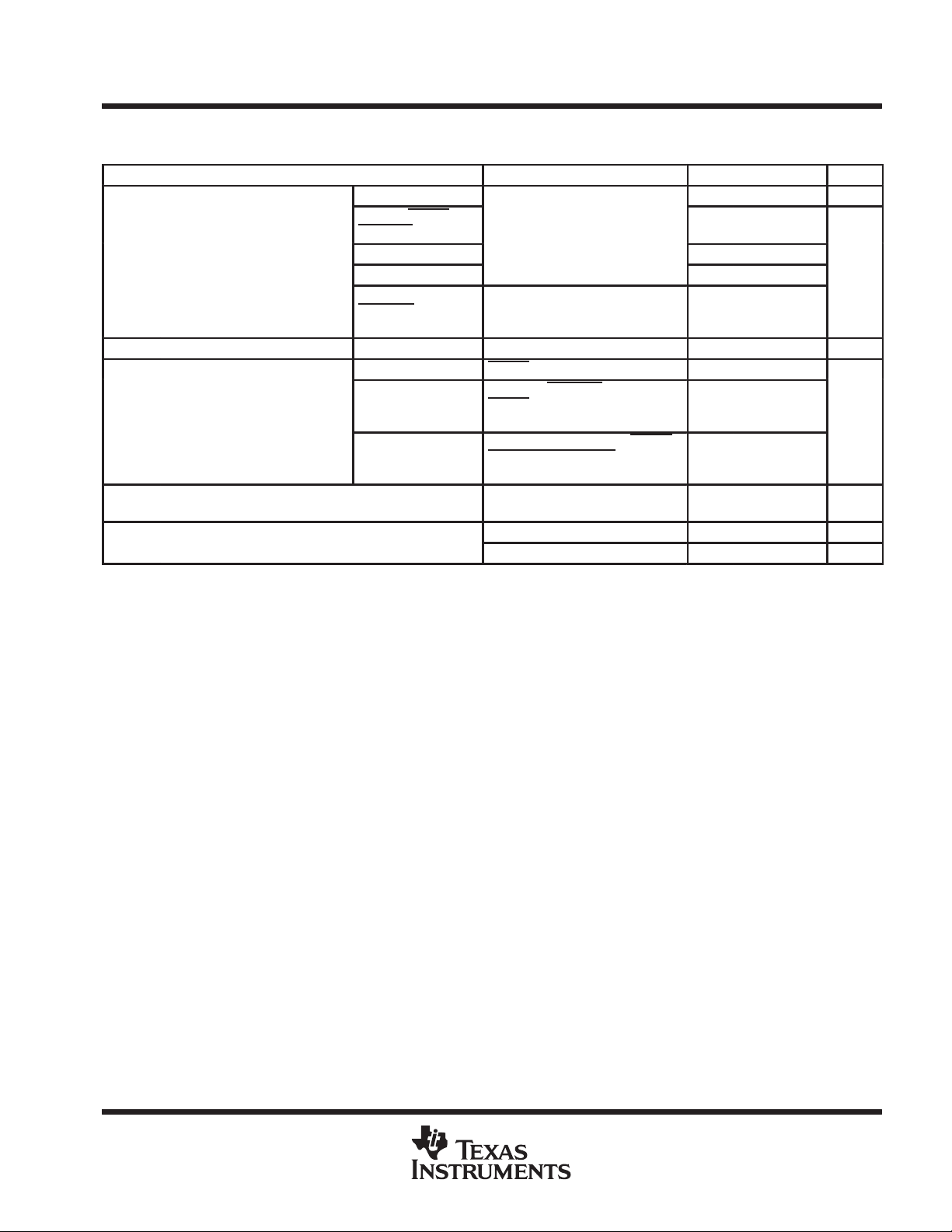
Table 1. Output Test Enabling (No Clock Input)
BUS CONTROL INPUT(s)
INPUT(s) OUTPUT TEST RSTFLTR RESET BBSY– BBSY+ ABSY– DSENS
ATN, ACK, MSG, C/D, REQ, I/O A B H H L
ATN, ACK, MSG, C/D, REQ, I/O B A H L L
RST A B L → H H L H H
RST B A L → H H L H H
SEL, BSY B A L H L → H
SEL, BSY B H H L H
TIMEOUT N/A H L L
DRVBUS
TIMEOUT N/A Z H L
†
For these conditions, DRVBUS = BSEL or BBSY and TIMEOUT together.
†
BBSY–/ BBSY+,
BSEL–/BSEL+,
TIMEOUT
DRVBUS H L L
12
POST OFFICE BOX 655303 • DALLAS, TEXAS 75265
Page 13

SCSI DIFFERENTIAL CONVERTER-CONTROL
SLLS323A – NOVEMBER 1999 – REVISED JANUARY 2000
PARAMETER MEASUREMENT INFORMATION
SN75970B
TIMEOUT
Input
V
CC
1.5 V
0 V
DRVBUS
15 pF
Input Output
V
1.5 V
V
t0 t0or t
Output
OH
OL
P
t
P
RSTFLTR
DSENS,
BSEL, BBSY
TEST
RESET
TIMEOUT
DRVBUS
t
PHL
Figure 5. TIMEOUT to DRVBUS Delay Time Test Circuit and Timing Definitions
t
PLH
POST OFFICE BOX 655303 • DALLAS, TEXAS 75265
13
Page 14

SN75970B
SCSI DIFFERENTIAL CONVERTER-CONTROL
SLLS323A – NOVEMBER 1999 – REVISED JANUARY 2000
PARAMETER MEASUREMENT INFORMATION
A–
Input
5 V
15 pF
75 Ω
165 Ω
B–
Output
B+
RSTFLTR
DSENS
TEST
RESET
CLK20
(see Note A)
3 V
1.5 V
0 V
165 Ω
Input Output
V
OD(H)
≈ –0.925 V
t0 t0or enable disable
15 pF
0.5 V
14
ARST–
ABSY– or ASEL–
t
en
BRST
t
dis
BBSY or BSEL
NOTE A: These are asynchronous events and do not necessarily align with clock edges.
t
en
t
dis
Figure 6. A-Side to B-Side Enable and Disable Delay Time Test Circuit and Timing Definitions
POST OFFICE BOX 655303 • DALLAS, TEXAS 75265
Page 15

SCSI DIFFERENTIAL CONVERTER-CONTROL
ООООООООО
ООООООООО
ООООООООО
ООООООООО
ООООООООО
ООООООООО
SLLS323A – NOVEMBER 1999 – REVISED JANUARY 2000
PARAMETER MEASUREMENT INFORMATION
SN75970B
3 V
1.5 V
0 V
RSTFLTR
DSENS
TEST
RESET
CLK40
(See Note A)
BRST–
1.5 V
B–
B+
15 pF
A–
Output
V
OH
1.5 V
V
OL
Input Output
Input
t0 t0or delay delay
Reset Bus Free
Arbitration
to Select 1
BBSY–
BSEL–
t
en1
t
dis1
ARST–
t
en3
t
dis3
t
en2
t
dis2
t
en4
ABSY–
ASEL–
NOTE A: These are asynchronous events and do not necessarily align with clock edges.
Figure 7. B-Side to A-Side Enable and Disable Delay Time Test Circuit and Timing Definitions
POST OFFICE BOX 655303 • DALLAS, TEXAS 75265
15
Page 16

SN75970B
SCSI DIFFERENTIAL CONVERTER-CONTROL
SLLS323A – NOVEMBER 1999 – REVISED JANUARY 2000
APPLICATION INFORMATION
To correctly set the direction of the SCSI bus signals, the SN75970B must follow the activity on the bus. An
asynchronous, 5-state controller watches the state of all the bus control signals, sets the direction of each
control signal as needed, and generates the DRVBUS and SDB outputs to control one or two external
SN75971B SCSI differential converter-data devices. The controller never generates the data driven on a bus
signal; it only enables the drivers. The clock input implements a 400-ns timer that is not part of the controller
itself. Controller-state transitions occur immediately when all the transition conditions are met. Note that the
frequency of the supplied clock, either 20 MHz or 40 MHz, must be correct in order to meet the SCSI
specifications.
As shown in Figure 8, after reset, the controller begins in the bus free state. In case the controller was attached
to an active differential bus, it waits for the SCSI bus free condition, defined as when BBSY and BSEL are
deasserted for 400 ns. While waiting for the SCSI bus free condition, the state of BBSY and BSEL passes
through to the A side. The A side bus device cannot take part in bus activity during this condition before the SCSI
bus free condition. Once SCSI bus free is detected, the SCSI arbitration state is entered. Both ABSY and BBSY
are enabled; thus when either signal asserts, both drivers turn on and both signals remain asserted until this
state is left. Normally the SCSI arbitration state ends after the winner of arbitration asserts BSEL. This would
cause the controller to go to the select 1 state. However, when BSEL is not asserted, a timeout would eventually
be detected and cause a reset of the controller. In the select 1 state two latches are open, DSEL_LATCH and
RESEL_LA TCH. The first latch captures the state of BSEL so that following states can determine whether the
arbitration winner was on the A side or B side.
16
POST OFFICE BOX 655303 • DALLAS, TEXAS 75265
Page 17

Bus Free
State
A
RESET
SCSI DIFFERENTIAL CONVERTER-CONTROL
SLLS323A – NOVEMBER 1999 – REVISED JANUARY 2000
APPLICATION INFORMATION
Enable ABSY and ASEL
BBSY = BSEL = 0?
SN75970B
NO
400 ns of
SCSI Bus Free Condition
YES
SCSI
Arbitration
State
Select 1
State
Select 2 State
ASEL or
YES
Set RESEL_LA TCH to AI/O DSEL_LATCH = 1?
YES
NO
ASEL = 1?
(DSEL_LATCH and
BSEL)?
NO
NO YES
BBSY?
Enable A Side
NO
NO
400 ns of
BBSY = 0?
YES
ABSY = 1 And
BBSY = 0?
YES
YES
Enable ABSY and BBSY
Set DSEL_LATCH to BSEL
Set RESEL_LA TCH to AI/O
NO
Enable B Side
400 ns of
ABSY = 0?
YES
Continued on Figure 9
NO
TIMEOUT?
NO
YES
RESET
Figure 8. Bus Free, SCSI Arbitration, and Select 1 State Flow Chart
The second latch captures the state of AI/O, this is true during a reselection phase but not during the selection
phase. When the bus is in the selection or reselection phase, the controller enters the select 1 state. There are
three possible flows depending on bus events. The first flow is that the SCSI controller on the A side won the
arbitration and asserted ASEL. In this event DSEL_LA TCH would not be set. The controller passes all signals
to the B side and waits for ABSY to deassert for 400 ns, indicating that the A side controller is selecting or
reselecting a device on the B side. The object of the A side controller must be on the B side since only one device
is allowed on the A side.
The second possible flow is that DSEL_LA TCH is set, indicating that the arbitration winner is on the B side, and
the winner is selecting or reselecting the device on the A side. The controller passes all signals to the A side
and waits for BBSY to deassert for 400 ns. When the A side controller responds by asserting ABSY , the controller
detects ABSY asserted and BBSY deasserts and goes to the select 2 state.
POST OFFICE BOX 655303 • DALLAS, TEXAS 75265
17
Page 18

SN75970B
SCSI DIFFERENTIAL CONVERTER-CONTROL
SLLS323A – NOVEMBER 1999 – REVISED JANUARY 2000
APPLICATION INFORMATION
The third possible flow is that a device on the B side won the arbitration and is selecting or reselecting another
device on the B side. DSEL_LA TCH is set, and 400 ns of BBSY is asserted first by the object of the selection
or reselection. Since ASEL is still asserted, the controller remains in the select 1 state throughout the selection
or reselection. If the BBSY deassertion is missed by the timer, again the controller remains in the select 1 state.
Once the transfer state is entered, BBSY is asserted and BSEL is dropped. This again returns the controller
to a select 1 state. At the end of the transfer both BBSY and BSEL are deasserted. After the timer limit is reached,
the controller goes to the arbitration state for the next bus arbitration.
The controller enters the select 2 state (see Figure 9) during the selection or reselection phases when the
initiator and terminator are on the opposite side of SDCC. In this state the RESEL_LA TCH is closed, capturing
the value of the I/O. When RESEL_LA TCH is one, reselection is indicated. When RESEL_LA TCH equals zero,
a selection is indicated. RESEL_LA TCH, along with the DSEL_LATCH, now defines which side the initiator is
on and therefore what direction to establish for all the bus signals. The target must be on the other side; if both
target and initiator were on the B side, the select 2 state would never be entered.
When the RESEL_LATCH is zero, indicating a selection, the connection is not made. When DSEL_LATCH is
one, the initiator is on the B side and the control lines it drives have their A side drivers enabled. These terminals
are the initiator group of ACK and A TN along with SEL. The other terminals are driven by the target and have
the B side drivers enabled. They are the target group of REQ, MSG, C/D, and I/O, along with BSY. When
DSEL_LATCH is zero the connection is reversed. Since transfer states are not started, DRVBUS is set to 1,
indicating that the data transceiver chips should not take their direction control from SDB and should be actively
negated. SDB is generated from I/O and is the bus signal that determines data transfer direction. In this case
it indicates the selection phase, the controller immediately transfers to the transfer state, where exactly the same
actions are done.
When the RESEL_LA TCH is 1 indicating a reselection, there are one or more actions before information states
can be entered. When the target reselects the initiator, the initiator responds by asserting BSY. Once the
connection is made, the assertion of BSY must be changed over to the target, and the controller must reverse
the BSY driver direction. It does this when SEL deasserts by transferring to the transfer state where the BSY
direction is reversed. In the select 2 state all the control line directions are set as appropriate, except that
DRVBUS is not yet asserted. In the transfer state DRBVUS is set as well.
The controller remains in the transfer state during all other SCSI states. When a bus free state is detected, it
goes back to the arbitration state to wait for the next activity. Note that after BBSY and BSEL deassert, the
controller continues to actively drive the control lines and the data lines through DRVBUS until 400 ns of
continuous deassertion is detected. The drivers are turned off only when the state change occurs.
Figure 10 shows a typical system configuration. The timeout function used in the arbitration state is
implemented with a resistor and capacitor connected to the TIMEOUT
terminal. During reset and whenever the
timer is not in use, the terminal is driven to VCC. The timer starts when the driver turns off, allowing the capacitor
to charge and the TIMEOUT terminal to drop to ground. When V
is reached, the driver turns on, discharging
IT-
the capacitor and returning TIMEOUT to VCC. A timeout event is declared after the driver turns back on and
TIMEOUT exceeds V
IT+
.
RST can be asserted on either the A or B side, and is driven to the other side. The drive to the other side is
controlled by a bidirectional latch. When one side asserts, the other side is asserted and a latch is set to that
direction. When the first side deasserts, the driver turns off, but the direction is held until both sides are
deasserted. Only then can the direction change.
18
POST OFFICE BOX 655303 • DALLAS, TEXAS 75265
Page 19

SCSI DIFFERENTIAL CONVERTER-CONTROL
SLLS323A – NOVEMBER 1999 – REVISED JANUARY 2000
APPLICATION INFORMATION
SN75970B
Select 1 State
Select 2
State
Enable BBSY , BINIT,
ASEL, And ATARG
YES
BSEL = 1?
NO
YES
DSEL_LATCH = 1?
Enable ABSY , AINIT,
BSEL, And BTARG
ASEL = 1?
YES
NO
NO
Enable BBSY , BT ARG,
YES
YES
DRVBUS = 1
SDB = AI/O
ASEL, And AINIT
DSEL_LATCH = 1?
YES
Continued From Figure 8
YES
YES
RESEL_LA TCH = 1?
DSEL_LATCH = 1?
Enable ABSY , A TARG,
BSEL, And BINIT
NO
RESEL_LA TCH = 1?RESEL_LA TCH = 1?
NO
NO
DRVBUS = 1
SDB = BI/O
Transfer
State
NO
DRVBUS = 1, SDB = AI/O
Enable BBSY , BT ARG,
ASEL, And AINIT
NO
400 ns of
BBSY = BSEL = 0?
YES
A
(On Figure 8)
DRVBUS = 1, SDB = BI/O
Enable ABSY , A TARG,
BSEL, And BINIT
Figure 9. SCSI Select 1, Select 2, and Transfer State Flow Chart
NO
POST OFFICE BOX 655303 • DALLAS, TEXAS 75265
19
Page 20

SN75970B
SCSI DIFFERENTIAL CONVERTER-CONTROL
SLLS323A – NOVEMBER 1999 – REVISED JANUARY 2000
APPLICATION INFORMATION
The SCSI bus signal RST does not directly clear SDCC internal logic. Instead, the RSTFL TR terminal can be
connected as ARST– so that a bus reset clears SDCC. RSTFL TR clears the internal controller but does not clear
the RST bidirectional latch. By connecting these terminal externally through a RC filter as shown in Figure 8,
noise pulses on the bus may be filtered as recommended by the SCSI-2 specification.
DIFFSENS
±BSY
±SEL
±RST
±I/O
±MSG
±C/D
±REQ
±ATN
±ACK
3
DSENS
6
8
4
BBSY±
BSEL±
RST±
BI/O±
BMSG±
BC/D±
BREQ±
BATN±
BACK±
7
Test
4
CLK40
(see Note A)
DRVBUS SDB
SN75970B
AMSG–
RSTFLTR
X1/CLK20
TIMEOUT
ABSY–
ASEL–
AI/O–
AC/D–
AREQ–
AATN–
AACK–
ARST–
RESET
X2
–BSY
–SEL
8
–MSG
–C/D
–REQ
–ATN
–ACK
–RST
1
2
RESET
(From System)
55
–I/O
20 MHz
(see Note A)
Optional
(see Note B)
V
CC
SCSI Controller
20 kΩ
1000 pF
0.022 µF
205 kΩ
±DB(7–0)
±DBP(0)
DIFFSENS
±DB(15–8)
±DBP(1)
DIFFSENS
NOTES: A. When using the 40 MHz clock input, X1 must be connected to VCC.
B. The oscillator cell of the SN75970B is for a series-resonant crystal and needs approximately 10 pF (including fixture capacitance)
from X1 and X2 to ground in order to function.
16
2
DRVBUS
16
2
SN75971B
SDB
SN75971B
8
8
–DB(7–0)
RESET
–DB(15–8)
RESET
Figure 10. Typical Application of the SN75970B and SN75971B
20
POST OFFICE BOX 655303 • DALLAS, TEXAS 75265
–DBP(0)
–DBP(1)
Page 21

SN75970B
SCSI DIFFERENTIAL CONVERTER-CONTROL
SLLS323A – NOVEMBER 1999 – REVISED JANUARY 2000
MECHANICAL INFORMATION
DGG (R-PDSO-G**) PLASTIC SMALL-OUTLINE PACKAGE
48 PIN SHOWN
0,50
48
1
1,20 MAX
0,27
0,17
25
24
A
0,15
0,05
0,08
M
8,30
6,20
7,90
6,00
Seating Plane
0,10
0,15 NOM
Gage Plane
0,25
0°–8°
0,75
0,50
DIM
NOTES: A. All linear dimensions are in millimeters.
B. This drawing is subject to change without notice.
C. Body dimensions do not include mold protrusion not to exceed 0,15.
D. Falls within JEDEC MO-153
PINS **
A MAX
A MIN
48
12,60
12,40
56
14,10
13,90
64
17,10
16,90
4040078/F 12/97
POST OFFICE BOX 655303 • DALLAS, TEXAS 75265
21
Page 22

SN75970B
SCSI DIFFERENTIAL CONVERTER-CONTROL
SLLS323A – NOVEMBER 1999 – REVISED JANUARY 2000
MECHANICAL INFORMATION
DL (R-PDSO-G**) PLASTIC SMALL-OUTLINE PACKAGE
48 PIN SHOWN
48
PINS **
DIM
A MAX
0.025 (0,635)
0.012 (0,305)
0.008 (0,203)
1
A
0.005 (0,13)
25
0.299 (7,59)
0.291 (7,39)
24
M
0.420 (10,67)
0.395 (10,03)
A MIN
0.006 (0,15) NOM
0°–8°
0.380
(9,65)
0.370
(9,40)
Gage Plane
4828
0.630
(16,00)
0.620
(15,75)
56
0.730
(18,54)
0.720
(18,29)
0.010 (0,25)
0.040 (1,02)
0.020 (0,51)
0.110 (2,79) MAX
NOTES: A. All linear dimensions are in inches (millimeters).
B. This drawing is subject to change without notice.
C. Body dimensions do not include mold flash or protrusion not to exceed 0.006 (0,15).
0.008 (0,20) MIN
Seating Plane
0.004 (0,10)
4040048/B 02/95
22
POST OFFICE BOX 655303 • DALLAS, TEXAS 75265
Page 23

PACKAGE OPTION ADDENDUM
www.ti.com
5-Oct-2007
PACKAGING INFORMATION
Orderable Device Status
(1)
Package
Type
Package
Drawing
Pins Package
Qty
Eco Plan
SN75970B1DL ACTIVE SSOP DL 56 20 Green (RoHS &
no Sb/Br)
SN75970B1DLG4 ACTIVE SSOP DL 56 20 Green (RoHS &
no Sb/Br)
SN75970B1DLR ACTIVE SSOP DL 56 1000 Green (RoHS &
no Sb/Br)
SN75970B1DLRG4 ACTIVE SSOP DL 56 1000 Green (RoHS &
no Sb/Br)
SN75970B2DGG ACTIVE TSSOP DGG 56 35 Green (RoHS &
no Sb/Br)
SN75970B2DGGG4 ACTIVE TSSOP DGG 56 35 Green (RoHS &
no Sb/Br)
SN75970B2DGGR ACTIVE TSSOP DGG 56 2000 Green (RoHS &
no Sb/Br)
SN75970B2DGGRG4 ACTIVE TSSOP DGG 56 2000 Green (RoHS &
no Sb/Br)
SN75970B2DL ACTIVE SSOP DL 56 20 Green (RoHS &
no Sb/Br)
SN75970B2DLG4 ACTIVE SSOP DL 56 20 Green (RoHS &
no Sb/Br)
SN75970B2DLR ACTIVE SSOP DL 56 1000 Green (RoHS &
no Sb/Br)
SN75970B2DLRG4 ACTIVE SSOP DL 56 1000 Green (RoHS &
no Sb/Br)
(1)
The marketing status values are defined as follows:
ACTIVE: Product device recommended for new designs.
LIFEBUY: TI has announced that the device will be discontinued, and a lifetime-buy period is in effect.
NRND: Not recommended for new designs. Device is in production to support existing customers, but TI does not recommend using this part in
a new design.
PREVIEW: Device has been announced but is not in production. Samples may or may not be available.
OBSOLETE: TI has discontinued the production of the device.
(2)
Lead/Ball Finish MSL Peak Temp
CU NIPDAU Level-2-260C-1 YEAR
CU NIPDAU Level-2-260C-1 YEAR
CU NIPDAU Level-2-260C-1 YEAR
CU NIPDAU Level-2-260C-1 YEAR
CU NIPDAU Level-2-260C-1 YEAR
CU NIPDAU Level-2-260C-1 YEAR
CU NIPDAU Level-2-260C-1 YEAR
CU NIPDAU Level-2-260C-1 YEAR
CU NIPDAU Level-2-260C-1 YEAR
CU NIPDAU Level-2-260C-1 YEAR
CU NIPDAU Level-2-260C-1 YEAR
CU NIPDAU Level-2-260C-1 YEAR
(3)
(2)
Eco Plan - The planned eco-friendly classification: Pb-Free (RoHS), Pb-Free (RoHS Exempt), or Green (RoHS & no Sb/Br) - please check
http://www.ti.com/productcontent for the latest availability information and additional product content details.
TBD: The Pb-Free/Green conversion plan has not been defined.
Pb-Free (RoHS): TI's terms "Lead-Free" or "Pb-Free" mean semiconductor products that are compatible with the current RoHS requirements
for all 6 substances, including the requirement that lead not exceed 0.1% by weight in homogeneous materials. Where designed to be soldered
at high temperatures, TI Pb-Free products are suitable for use in specified lead-free processes.
Pb-Free (RoHS Exempt): This component has a RoHS exemption for either 1) lead-based flip-chip solder bumps used between the die and
package, or 2) lead-based die adhesive used between the die and leadframe. The component is otherwise considered Pb-Free (RoHS
compatible) as defined above.
Green (RoHS & no Sb/Br): TI defines "Green" to mean Pb-Free (RoHS compatible), and free of Bromine (Br) and Antimony (Sb) based flame
retardants (Br or Sb do not exceed 0.1% by weight in homogeneous material)
(3)
MSL, Peak Temp. -- The Moisture Sensitivity Level rating according to the JEDEC industry standard classifications, and peak solder
temperature.
Important Information and Disclaimer:The information provided on this page represents TI's knowledge and belief as of the date that it is
provided. TI bases its knowledge and belief on information provided by third parties, and makes no representation or warranty as to the
accuracy of such information. Efforts are underway to better integrate information from third parties. TI has taken and continues to take
reasonable steps to provide representative and accurate information but may not have conducted destructive testing or chemical analysis on
incoming materials and chemicals. TI and TI suppliers consider certain information to be proprietary, and thus CAS numbers and other limited
information may not be available for release.
Addendum-Page 1
Page 24

PACKAGE OPTION ADDENDUM
www.ti.com
In no event shall TI's liability arising out of such information exceed the total purchase price of the TI part(s) at issue in this document sold by TI
to Customer on an annual basis.
5-Oct-2007
Addendum-Page 2
Page 25

PACKAGE MATERIALS INFORMATION
www.ti.com
TAPE AND REEL INFORMATION
11-Mar-2008
*All dimensions are nominal
Device Package
SN75970B1DLR SSOP DL 56 1000 330.0 32.4 11.35 18.67 3.1 16.0 32.0 Q1
SN75970B2DGGR TSSOP DGG 56 2000 330.0 24.4 8.6 15.6 1.8 12.0 24.0 Q1
SN75970B2DLR SSOP DL 56 1000 330.0 32.4 11.35 18.67 3.1 16.0 32.0 Q1
Type
Package
Drawing
Pins SPQ Reel
Diameter
(mm)
Reel
Width
W1 (mm)
A0 (mm) B0 (mm) K0 (mm) P1
(mm)W(mm)
Pin1
Quadrant
Pack Materials-Page 1
Page 26

PACKAGE MATERIALS INFORMATION
www.ti.com
11-Mar-2008
*All dimensions are nominal
Device Package Type Package Drawing Pins SPQ Length (mm) Width (mm) Height (mm)
SN75970B1DLR SSOP DL 56 1000 346.0 346.0 49.0
SN75970B2DGGR TSSOP DGG 56 2000 346.0 346.0 41.0
SN75970B2DLR SSOP DL 56 1000 346.0 346.0 49.0
Pack Materials-Page 2
Page 27

IMPORTANT NOTICE
Texas Instruments Incorporated and its subsidiaries (TI) reserve the right to make corrections, modifications, enhancements, improvements,
and other changes to its products and services at any time and to discontinue any product or service without notice. Customers should
obtain the latest relevant information before placing orders and should verify that such information is current and complete. All products are
sold subject to TI’s terms and conditions of sale supplied at the time of order acknowledgment.
TI warrants performance of its hardware products to the specifications applicable at the time of sale in accordance with TI’s standard
warranty. Testing and other quality control techniques are used to the extent TI deems necessary to support this warranty. Except where
mandated by government requirements, testing of all parameters of each product is not necessarily performed.
TI assumes no liability for applications assistance or customer product design. Customers are responsible for their products and
applications using TI components. To minimize the risks associated with customer products and applications, customers should provide
adequate design and operating safeguards.
TI does not warrant or represent that any license, either express or implied, is granted under any TI patent right, copyright, mask work right,
or other TI intellectual property right relating to any combination, machine, or process in which TI products or services are used. Information
published by TI regarding third-party products or services does not constitute a license from TI to use such products or services or a
warranty or endorsement thereof. Use of such information may require a license from a third party under the patents or other intellectual
property of the third party, or a license from TI under the patents or other intellectual property of TI.
Reproduction of TI information in TI data books or data sheets is permissible only if reproduction is without alteration and is accompanied
by all associated warranties, conditions, limitations, and notices. Reproduction of this information with alteration is an unfair and deceptive
business practice. TI is not responsible or liable for such altered documentation. Information of third parties may be subject to additional
restrictions.
Resale of TI products or services with statements different from or beyond the parameters stated by TI for that product or service voids all
express and any implied warranties for the associated TI product or service and is an unfair and deceptive business practice. TI is not
responsible or liable for any such statements.
TI products are not authorized for use in safety-critical applications (such as life support) where a failure of the TI product would reasonably
be expected to cause severe personal injury or death, unless officers of the parties have executed an agreement specifically governing
such use. Buyers represent that they have all necessary expertise in the safety and regulatory ramifications of their applications, and
acknowledge and agree that they are solely responsible for all legal, regulatory and safety-related requirements concerning their products
and any use of TI products in such safety-critical applications, notwithstanding any applications-related information or support that may be
provided by TI. Further, Buyers must fully indemnify TI and its representatives against any damages arising out of the use of TI products in
such safety-critical applications.
TI products are neither designed nor intended for use in military/aerospace applications or environments unless the TI products are
specifically designated by TI as military-grade or "enhanced plastic." Only products designated by TI as military-grade meet military
specifications. Buyers acknowledge and agree that any such use of TI products which TI has not designated as military-grade is solely at
the Buyer's risk, and that they are solely responsible for compliance with all legal and regulatory requirements in connection with such use.
TI products are neither designed nor intended for use in automotive applications or environments unless the specific TI products are
designated by TI as compliant with ISO/TS 16949 requirements. Buyers acknowledge and agree that, if they use any non-designated
products in automotive applications, TI will not be responsible for any failure to meet such requirements.
Following are URLs where you can obtain information on other Texas Instruments products and application solutions:
Products Applications
Amplifiers amplifier.ti.com Audio www.ti.com/audio
Data Converters dataconverter.ti.com Automotive www.ti.com/automotive
DSP dsp.ti.com Broadband www.ti.com/broadband
Clocks and Timers www.ti.com/clocks Digital Control www.ti.com/digitalcontrol
Interface interface.ti.com Medical www.ti.com/medical
Logic logic.ti.com Military www.ti.com/military
Power Mgmt power.ti.com Optical Networking www.ti.com/opticalnetwork
Microcontrollers microcontroller.ti.com Security www.ti.com/security
RFID www.ti-rfid.com Telephony www.ti.com/telephony
RF/IF and ZigBee® Solutions www.ti.com/lprf Video & Imaging www.ti.com/video
Mailing Address: Texas Instruments, Post Office Box 655303, Dallas, Texas 75265
Copyright © 2008, Texas Instruments Incorporated
Wireless www.ti.com/wireless
 Loading...