

SN75476 THRU SN75478
DUAL PERIPHERAL DRIVERS
SLRS025A – DECEMBER 1976 – REVISED NOVEMBER 1995
Copyright 1995, Texas Instruments Incorporated
1
POST OFFICE BOX 655303 • DALLAS, TEXAS 75265
POST OFFICE BOX 1443
• HOUSTON, TEXAS 77251–1443
• Characterized for Use to 300 mA
• No Output Latch-Up at 55 V (After
Conducting 300 mA)
• High-Voltage Outputs (100 V Typ)
• Output Clamp Diodes for Transient
Suppression (300 mA, 70 V)
• TTL- or MOS-Compatible Diode-Clamped
Inputs
• pnp Transistor Inputs Reduce Input Current
• Standard Supply Voltage
• Suitable for Hammer-Driver Applications
• Plastic DIP (P) With Copper-Lead Frame
Provides Cooler Operation and Improved
Reliability
description
The SN75476 through SN75478 are dual
peripheral drivers designed for use in systems that
require high current, high voltage, and fast
switching times. The SN75476, SN75477, and
SN75478 provide AND, NAND, and OR drivers
respectively. These devices have diode-clamped
inputs as well as high-current, high-voltage clamp
diodes on the outputs for inductive transient
protection.
The SN75476, SN75477, and SN75478 drivers
are characterized for operation from 0°C to 70°C.
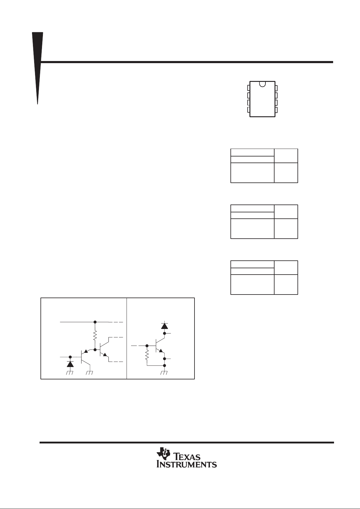
schematics of inputs and outputs
V
CC
Input
CLAMP
Output
GND
EQUIVALENT
OF EACH INPUT
TYPICAL
OF ALL OUTPUTS
1
2
3
4
8
7
6
5
S
1A
1Y
GND
V
CC
2A
2Y
CLAMP
D OR P PACKAGE
(TOP VIEW)
H = high level, L = low level
X = irrelevant
INPUTS
OUTPUT
Y
SN75476
(each AND driver)
AS
H
L
X
H
X
L
H
L
L
Function Tables
INPUTS
OUTPUT
Y
SN75477
(each NAND driver)
AS
H
L
X
H
X
L
L
H
H
INPUTS
OUTPUT
Y
SN75478
(each OR driver)
AS
H
X
L
X
H
L
H
H
L
PRODUCTION DATA information is current as of publication date.
Products conform to specifications per the terms of Texas Instruments
standard warranty. Production processing does not necessarily include
testing of all parameters.
SN75476 THRU SN75478
DUAL PERIPHERAL DRIVERS
SLRS025A – DECEMBER 1976 – REVISED NOVEMBER 1995
2
POST OFFICE BOX 655303 • DALLAS, TEXAS 75265
POST OFFICE BOX 1443
• HOUSTON, TEXAS 77251–1443
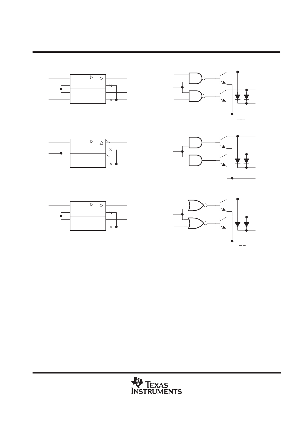
logic symbols
†
logic diagrams (positive logic)
†
These symbols are in accordance with ANSI/IEEE Std 91-1984
and IEC publication 617-12.
2A
S
1A
7
1
2
GND
CLAMP
2Y
1Y
4
5
6
3
CLAMP
CLAMP
2Y
1Y
7
1
2
2A
S
1A
5
6
3
3
6
5
1A
S
2A
2
1
7
1Y
2Y
CLAMP
CLAMP
3
6
5
4
1Y
2Y
CLAMP
GND
2
1
7
1A
S
2A
2A
S
1A
7
1
2
GND
CLAMP
2Y
1Y
4
5
6
3
CLAMP
CLAMP
2Y
1Y
7
1
2
2A
S
1A
5
6
3
&
&
≥1
SN75476
SN75476
Positive Logic: Y = AS or A
+S
SN75477
SN75477
Positive Logic: Y = AS
or A+S
SN75478
SN75478
Positive Logic: Y = A+S or A
S
SN75476 THRU SN75478
DUAL PERIPHERAL DRIVERS
SLRS025A – DECEMBER 1976 – REVISED NOVEMBER 1995
3
POST OFFICE BOX 655303 • DALLAS, TEXAS 75265
POST OFFICE BOX 1443
• HOUSTON, TEXAS 77251–1443
absolute maximum ratings over operating free-air temperature range (unless otherwise noted)
Supply voltage, VCC (see Note 1) 7 V. . . . . . . . . . . . . . . . . . . . . . . . . . . . . . . . . . . . . . . . . . . . . . . . . . . . . . . . . . . . .
Input voltage, VI 5.5 V. . . . . . . . . . . . . . . . . . . . . . . . . . . . . . . . . . . . . . . . . . . . . . . . . . . . . . . . . . . . . . . . . . . . . . . . . .
Continuous output current (see Note 2) 400 mA. . . . . . . . . . . . . . . . . . . . . . . . . . . . . . . . . . . . . . . . . . . . . . . . . . . .
Peak output current: tw ≤ 10 ms, duty cycle ≤ 50% 500 mA. . . . . . . . . . . . . . . . . . . . . . . . . . . . . . . . . . . . . . . . . .
tw ≤ 30 ns, duty cycle ≤ 0.002% 3 A. . . . . . . . . . . . . . . . . . . . . . . . . . . . . . . . . . . . . . . . . . .
Output clamp current, I
OK
400 mA. . . . . . . . . . . . . . . . . . . . . . . . . . . . . . . . . . . . . . . . . . . . . . . . . . . . . . . . . . . . . . . .
Continuous total power dissipation See Dissipation Rating Table. . . . . . . . . . . . . . . . . . . . . . . . . . . . . . . . . . . . .
Operating free-air temperature range, TA 0°C to 70°C. . . . . . . . . . . . . . . . . . . . . . . . . . . . . . . . . . . . . . . . . . . . . .
Storage temperature range, T
stg
–65°C to 150°C. . . . . . . . . . . . . . . . . . . . . . . . . . . . . . . . . . . . . . . . . . . . . . . . . .
Lead temperature 1,6 mm (1/16 inch) from case for 10 seconds 260°C. . . . . . . . . . . . . . . . . . . . . . . . . . . . . . .
NOTES: 1. Voltage values are with respect to network GND.
2. Both halves of this dual circuit may conduct rated current simultaneously; however, power dissipation averaged over a short time
interval must fall within the continuous power dissipation ratings.
DISSIPATION RATING TABLE
T
≤ 25°C DERATING FACTOR T
= 70°C
PACKAGE
A
POWER RATING ABOVE TA = 25°CAPOWER RATING
D 725 mW 5.8 mW/°C 464 mW
P 1000 mW 8.0 mW/°C 640 mW
recommended operating conditions
MIN NOM MAX UNIT
Supply voltage, V
CC
4.5 5 5.5 V
High-level input voltage, V
IH
2 V
Low-level input voltage, V
IL
0.8 V
Operating free-air temperature, T
A
0 70 °C

SN75476 THRU SN75478
DUAL PERIPHERAL DRIVERS
SLRS025A – DECEMBER 1976 – REVISED NOVEMBER 1995
4
POST OFFICE BOX 655303 • DALLAS, TEXAS 75265
POST OFFICE BOX 1443
• HOUSTON, TEXAS 77251–1443
electrical characteristics over recommended operating free-air temperature range
PARAMETER TEST CONDITIONS MIN TYP†MAX UNIT
V
IK
Input clamp voltage II = –12 mA –0.95 –1.5 V
=
IOL = 100 mA 0.16 0.3
V
OL
Low-level output voltage
V
CC
= 4.5 V,
VIH = 2 V,
IOL = 175 mA 0.22 0.5
V
VIL = 0.8 V
IOL = 300 mA 0.33 0.6
V
O(BR)
Output breakdown voltage VCC = 4.5 V, IOH = 100 µA 70 100 V
V
R(K)
Output clamp reverse voltage VCC = 4.5 V, IR = 100 µA 70 100 V
V
F(K)
Output clamp forward voltage VCC = 4.5 V, IF = 300 mA 0.8 1.15 1.6 V
p
V
= 4.5 V, V
= 2 V,
IOHHigh-level output current
CC
,
VIL = 0.8 V,
IH
,
VOH = 70 V
1
100µA
I
IH
High-level input current VCC = 5.5 V, VI = 5.5 V 0.01 10 µA
p
A input
–80 –110
IILLow-level input current
S input
V
CC
=
5.5 V
,
V
I
=
0.8 V
–160 –220
µ
A
SN75476 VI = 5 V 10 17
I
CCH
Supply current, outputs high
SN75477
VCC = 5.5 V
VI = 0 10 17
mA
SN75478 VI = 5 V 10 17
SN75476 VI = 0 54 75
I
CCL
Supply current, outputs low
SN75477
VCC = 5.5 V
VI = 5 V 54 75
mA
SN75478 VI = 0 54 75
†
All typical values are at VCC = 5 V, TA = 25°C.
switching characteristics, VCC = 5 V, TA = 25°C
PARAMETER TEST CONDITIONS MIN TYP MAX UNIT
t
PLH
Propagation delay time, low-to-high-level output 200 350 ns
t
PHL
Propagation delay time, high-to-low-level output
C
= 15 pF, R
= 100 Ω,
200 350 ns
t
TLH
Transition time, low-to-high-level output
L
,
See Figure 1
L
,
50 125 ns
t
THL
Transition time, high-to-low-level output 90 125 ns
p
V
= 55 V, I
≈ 300 mA,
VOHHigh-level output voltage after switching
S
,
See Figure 2
O
,
V
S
–
18
mV

SN75476 THRU SN75478
DUAL PERIPHERAL DRIVERS
SLRS025A – DECEMBER 1976 – REVISED NOVEMBER 1995
5
POST OFFICE BOX 655303 • DALLAS, TEXAS 75265
POST OFFICE BOX 1443
• HOUSTON, TEXAS 77251–1443
PARAMETER MEASUREMENT INFORMATION
30 V
2.4 V
0.4 V
TEST CIRCUIT
A/S
S/A
SN75478
SN75476
SN75477
RL = 100 Ω
CL = 15 pF
(see Note B)
V
CC
2.7 V 2.7 V
1.5 V 1.5 V
0.7 V 0.7 V
50%50%
t
PHL
≤ 10 ns≤ 5 ns
3 V
0 V
V
OH
V
OL
Output
VOLTAGE WAVEFORMS
0.7 V
2.7 V
Input
t
PLH
10% 10%
90% 90%
t
THL
t
TLH
3 V
0 V
≤ 10 ns
≤ 5 ns
0.7 V
1.5 V
2.7 V
1.5 V
5 µs
SN75446
SN75448
SN75447
Pulse
Generator
(see Note A)
Input
Circuit
Under
Test
Output
Open
Input
NOTES: A. The pulse generator has the following characteristics: PRR = 100 kHz, ZO = 50 Ω.
B. CL includes probe and jig capacitance.
Figure 1. Test Circuit and Voltage Waveforms, Switching Characteristics

SN75476 THRU SN75478
DUAL PERIPHERAL DRIVERS
SLRS025A – DECEMBER 1976 – REVISED NOVEMBER 1995
6
POST OFFICE BOX 655303 • DALLAS, TEXAS 75265
POST OFFICE BOX 1443
• HOUSTON, TEXAS 77251–1443
PARAMETER MEASUREMENT INFORMATION
2 mH
Input
2.4 V
Output
0.4 V
TEST CIRCUIT
S
SN75478
SN75476
SN75477
VS = 55 V
CL = 15 pF
(see Note B)
5 V
90% 90%
1.5 V 1.5 V
10%
10%
≤ 10 ns≤ 5 ns
3 V
0 V
V
OH
V
OL
Output
VOLTAGE WAVEFORMS
10%
90%
Input
3 V
0 V
≤ 10 ns
≤ 5 ns
10%
1.5 V
90%
1.5 V
40 µs
SN75476
SN75478
SN75477
A
GND
Pulse
Generator
(see Note A)
Circuit
Under
Test
180 Ω
Input
NOTES: A. The pulse generator has the following characteristics: PRR = 12.5 kHz, ZO = 50 Ω.
B. CL includes probe and jig capacitance.
Figure 2. Latch-Up Test Circuit and Voltage Waveforms

IMPORTANT NOTICE
T exas Instruments and its subsidiaries (TI) reserve the right to make changes to their products or to discontinue
any product or service without notice, and advise customers to obtain the latest version of relevant information
to verify, before placing orders, that information being relied on is current and complete. All products are sold
subject to the terms and conditions of sale supplied at the time of order acknowledgement, including those
pertaining to warranty, patent infringement, and limitation of liability.
TI warrants performance of its semiconductor products to the specifications applicable at the time of sale in
accordance with TI’s standard warranty. Testing and other quality control techniques are utilized to the extent
TI deems necessary to support this warranty. Specific testing of all parameters of each device is not necessarily
performed, except those mandated by government requirements.
CERT AIN APPLICATIONS USING SEMICONDUCTOR PRODUCTS MAY INVOLVE POTENTIAL RISKS OF
DEATH, PERSONAL INJURY, OR SEVERE PROPERTY OR ENVIRONMENTAL DAMAGE (“CRITICAL
APPLICATIONS”). TI SEMICONDUCTOR PRODUCTS ARE NOT DESIGNED, AUTHORIZED, OR
WARRANTED TO BE SUITABLE FOR USE IN LIFE-SUPPORT DEVICES OR SYSTEMS OR OTHER
CRITICAL APPLICATIONS. INCLUSION OF TI PRODUCTS IN SUCH APPLICA TIONS IS UNDERSTOOD T O
BE FULLY AT THE CUSTOMER’S RISK.
In order to minimize risks associated with the customer’s applications, adequate design and operating
safeguards must be provided by the customer to minimize inherent or procedural hazards.
TI assumes no liability for applications assistance or customer product design. TI does not warrant or represent
that any license, either express or implied, is granted under any patent right, copyright, mask work right, or other
intellectual property right of TI covering or relating to any combination, machine, or process in which such
semiconductor products or services might be or are used. TI’s publication of information regarding any third
party’s products or services does not constitute TI’s approval, warranty or endorsement thereof.
Copyright 1998, Texas Instruments Incorporated
 Loading...