

Page 1
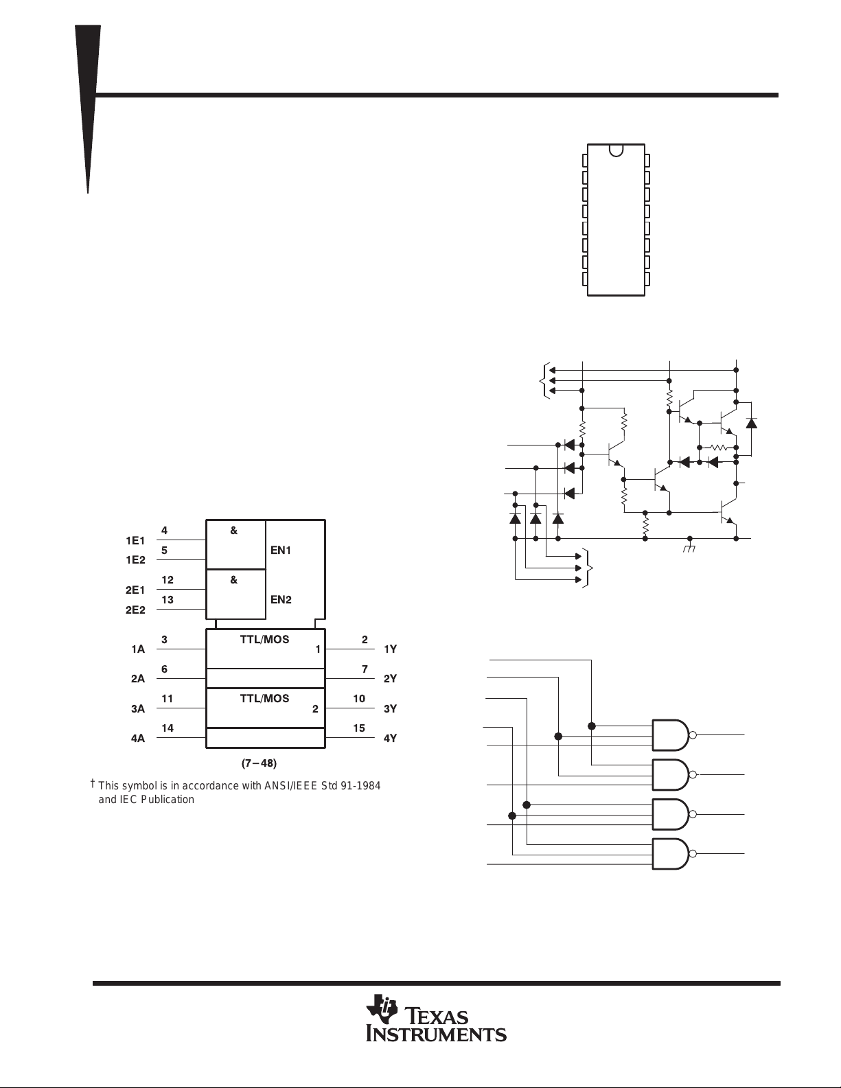
SN75374
QUADRUPLE MOSFET DRIVER
SLRS028 – SEPTEMBER 1988
• Quadruple Circuits Capable of Driving
High-Capacitance Loads at High Speeds
• Output Supply Voltage Range From 5 V
to 24 V
• Low Standby Power Dissipation
• V
description
logic symbol
Supply Maximizes Output Source
CC3
Voltage
The SN75374 is a quadruple NAND interface
circuit designed to drive power MOSFETs from
TTL inputs. It provides the high current and
voltage necessary to drive large capacitive loads
at high speeds.
The outputs can be switched very close to the
V
supply rail when V
CC2
than V
CC2
. V
can also be tied directly to V
CC3
is about 3 V higher
CC3
when the source voltage requirements are lower.
The SN75374 is characterized for operation from
0°C to 70°C.
†
CC2
D OR N PACKAGE
(TOP VIEW)
V
GND
CC2
1Y
1A
1E1
1E2
2A
2Y
1
2
3
4
5
6
7
8
schematic (each driver)
V
CC1
To Other
Drivers
Input A
Enable
E1
Enable
E2
16
15
14
13
12
11
10
V
CC1
4Y
4A
2E2
2E1
3A
3Y
9
V
CC3
V
CC3
V
CC2
Output
Y
4
1E1
5
1E2
12
2E1
13
2E2
3
1A
6
2A
11
3A
14
4A
†
This symbol is in accordance with ANSI/IEEE Std 91-1984
and IEC Publication 617-12
&
&
TTL/MOS
TTL/MOS
(7-48)
EN1
EN2
1
10
2
15
GND
To Other
Drivers
logic diagram (positive logic)
2
1Y
7
2Y
3Y
4Y
1E1
1E2
2E1
2E2
1A
2A
3A
4A
4
5
12
13
3
6
11
14
2
7
10
15
1Y
2Y
3Y
4Y
PRODUCTION DATA information is current as of publication date.
Products conform to specifications per the terms of Texas Instruments
standard warranty. Production processing does not necessarily include
testing of all parameters.
POST OFFICE BOX 655303 • DALLAS, TEXAS 75265
Copyright 1988, Texas Instruments Incorporated
3–1
Page 2
SN75374
PACKAGE
A
QUADRUPLE MOSFET DRIVER
SLRS028 – SEPTEMBER 1988
absolute maximum ratings over operating free-air temperature range (unless otherwise noted)
Supply voltage range of V
Supply voltage range of V
Supply voltage range of V
(see Note 1) –0.5 V to 7 V. . . . . . . . . . . . . . . . . . . . . . . . . . . . . . . . . . . . . . . . . . . .
CC1
–0.5 V to 25 V. . . . . . . . . . . . . . . . . . . . . . . . . . . . . . . . . . . . . . . . . . . . . . . . . . . . . .
CC2
–0.5 V to 30 V. . . . . . . . . . . . . . . . . . . . . . . . . . . . . . . . . . . . . . . . . . . . . . . . . . . . . .
CC3
Input voltage, VI 5.5 V. . . . . . . . . . . . . . . . . . . . . . . . . . . . . . . . . . . . . . . . . . . . . . . . . . . . . . . . . . . . . . . . . . . . . . . . . .
Peak output current, II (tw < 10 ms, duty cycle < 50%) 500 mA. . . . . . . . . . . . . . . . . . . . . . . . . . . . . . . . . . . . . . .
Continuous total power dissipation See Dissipation Rating Table. . . . . . . . . . . . . . . . . . . . . . . . . . . . . . . . . . . . .
Operating free-air temperature range, TA 0°C to 70°C. . . . . . . . . . . . . . . . . . . . . . . . . . . . . . . . . . . . . . . . . . . . . .
Storage temperature range, T
–65°C to 150°C. . . . . . . . . . . . . . . . . . . . . . . . . . . . . . . . . . . . . . . . . . . . . . . . . .
stg
Lead temperature 1,6 mm (1/16 inch) from case for 10 seconds 260°C. . . . . . . . . . . . . . . . . . . . . . . . . . . . . . .
NOTE 1: Voltage values are with respect to network ground terminal.
DISSIPATION RATING T ABLE
T
≤ 25°C DERATING FACTOR T
POWER RATING ABOVE TA = 25°CAPOWER RATING
D 950 mW 7.6 mW/°C 608 mW
N 1150 mW 9.2 mW/°C 736 mW
= 70° C
recommended operating conditions
MIN NOM MAX UNIT
Supply voltage, V
Supply voltage, V
Supply voltage, V
Voltage dif ference between supply voltages: V
High-level input voltage, V
Low-level input voltage, V
High-level output current, I
High-level output current, I
Operating free-air temperature, T
CC1
CC2
CC3
IH
IL
OH
OL
A
CC3
– V
CC2
4.75 5 5.25 V
4.75 20 24 V
V
CC2
0 4 10 V
2 V
0 70 °C
24 28 V
0.8 V
–10 mA
40 mA
3–2
POST OFFICE BOX 655303 • DALLAS, TEXAS 75265
Page 3
SN75374
VOHHigh-level output voltage
V
VOLLow-level output voltage
V
V
V
I
mA
1.5
V
I
V
V
1
mA
I
g
V
V
A
I
V
V
mA
I
y
4
8
I
y
CC1
,
CC2
,
CC3
,
2
0.25
mA
I
y
2.2
3.5
I
y
31
47
I
y
CC1
,
CC2
,
CC3
,
2
mA
I
y
16
27
I
y
,
,
0.25
V
CC1
5.25 V,
V
CC2
V, V
CC3
V,
A
0.5
I
y
0.25
CC1
CC2 CC3
mA
I
y
0.5
R
g
See Figure 1
QUADRUPLE MOSFET DRIVER
SLRS028 – SEPTEMBER 1988
electrical characteristics over recommended ranges of V
temperature (unless otherwise noted)
PARAMETER TEST CONDITIONS MIN TYP†MAX UNIT
V
IK
F
I
IH
IL
CC1(H)
CC2(H)
CC3(H)
CC1(L)
CC2(L)
CC3(L)
CC2(H)
I
CC3(H)
CC2(S)
CC3(S)
†
All typical values are at V
conditions.
Input clamp voltage II = –12 mA –1.5 V
V
p
p
Output clamp-diode
forward voltage
Input current at
maximum input voltage
CC1
Any A
Any E
Any A
Any E
= 5 V , V
CC2
High-level
input current
low-level
input current
Supply current from
V
, all outputs high
CC1
Supply current from V
V
, all outputs high
CC2
Supply current from
V
, all outputs high
CC3
Supply current from
V
, all outputs low
CC1
Supply current from V
V
, all outputs low
CC2
Supply current from
V
, all outputs low
CC1
Supply current from
V
, all outputs high
CC2
Supply current from
V
, all outputs high
CC3
Supply current from
V
, standby condition
CC2
Supply current from
V
, standby condition
CC3
= V
CC3
V
= V
CC3
V
= V
CC3
V
= V
CC3
VIH = 2 V, IOL = 10 mA 0.15 0.3
V
= 15 V to 28 V, VIH = 2 V, IOL = 40 mA 0.25 0.5
CC2
= 0,
I
= 5.5
I
= 2.4
I
= 0.4
I
= 5.25 V, V
All inputs at 0 V,
= 5.25 V, V
All inputs at 5 V,
= 5.25 V
V
All inputs at 0 V,
V
= 0,
CC1
All inputs at 0 V,
= 20 V , V
+ 3 V, VIL = 0.8 V, IOH = –100 µA V
CC2
+ 3 V, VIL = 0.8 V, IOH = –10 mA V
CC2
, VIL = 0.8 V, IOH = –50 µA V
CC2
, VIL = 0.8 V, IOH = –10 mA V
CC2
= 20
F
= 24 V, V
No load
= 24 V, V
No load
V
= 24 V,V
24
No load
V
= 24 V, V
CC2
No load
= 24 V , and TA = 25°C except for VOH for which V
CC3
CC3
CC1
= 28 V,
= 28 V,
= 24 V
24
= 24 V,
, V
CC2
, V
CC2
CC2
CC2
CC2
, and operating free-air
CC3
–
–0.3 V
–1.3 V
–1 V
–2.5 V
and V
CC2
0.1
CC2
–0.9
CC2
–0.7
CC2
–1.8
CC2
–1 –1.6
–2 –3.2
–2.
are as stated under test
CC3
40
80
µ
m
switching characteristics, V
t
DLH
t
DHL
t
PLH
t
PHL
t
TLH
t
THL
= 5 V, V
CC1
PARAMETER TEST CONDITIONS MIN TYP MAX UNIT
Delay time, low-to-high-level output 20 30 ns
Delay time, high-to-low-level output 10 20 ns
Propagation delay time, low-to-high-level output
Propagation delay time, high-to-low-level output
Transition time, low-to-high-level output
Transition time, high-to-low-level output 20 30 ns
POST OFFICE BOX 655303 • DALLAS, TEXAS 75265
CC2
= 20 V, V
= 24 V, TA = 25°C
CC3
CL = 200 pF
= 24 Ω,
D
See Fi
ure 1
10 40 60 ns
10 30 50 ns
20 30 ns
3–3
Page 4
SN75374
QUADRUPLE MOSFET DRIVER
SLRS028 – SEPTEMBER 1988
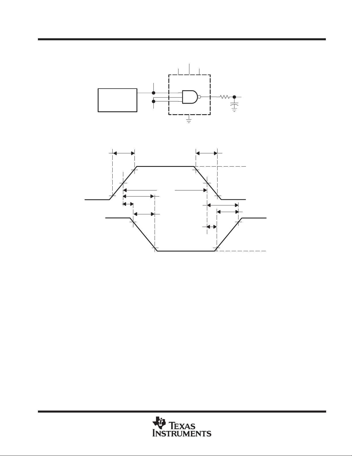
PARAMETER MEASUREMENT INFORMATION
5 V
24 V
20 V
Input
Output
Input
Pulse
Generator
(see Note A)
2.4 V
≤ 10 ns ≤ 10 ns
90% 90%
1.5 V 1.5 V
10%
t
DHL
V
–2 V
CC2
V
TEST CIRCUIT
0.5 µs
t
PHL
t
THL
CC1
V
CC3
GND
t
t
V
PLH
DLH
CC2
R
D
10%
Output
CL = 200 pF
(see Note B)
3 V
0 V
t
TLH
V
–2 V
CC2
V
OH
2 V
VOLTAGE WAVEFORMS
2 V
Figure 1. Test Circuit and Voltage Waveforms, Each Driver
NOTES: A. The pulse generator has the following characteristics: PRR = 1 MHz, ZO ≈ 50 Ω.
B. CL includes probe and jig capacitance.
V
OL
3–4
POST OFFICE BOX 655303 • DALLAS, TEXAS 75265
Page 5
TYPICAL CHARACTERISTICS
SN75374
QUADRUPLE MOSFET DRIVER
SLRS028 – SEPTEMBER 1988
V
CC2
– 0.5
–1
– 1.5
–2
OH
V
– 2.5
VOH – High-Level Output Voltage – V
–3
– 0.01
0.5
0.4
0.3
HIGH-LEVEL OUTPUT VOLTAGE
vs
HIGH-LEVEL OUTPUT CURRENT
V
= 5 V
CC1
V
= 20 V
CC2
V
= 24 V
CC3
VI = 0.8 V
– 0.1 – 10–1
IOH – High-Level Output Current – mA
Figure 2 Figure 3
LOW-LEVEL OUTPUT VOLTAGE
vs
LOW-LEVEL OUTPUT CURRENT
V
= 5 V
CC1
V
= 20 V
CC2
V
= 24 V
CC3
VI = 2 V
TA = 70°C
TA = 0°C
TA = 70°C
TA = 0°C
– 100
V
CC2
–0.5
–1
–1.5
–2
OH
V
–2.5
VOH – High-Level Output Voltage – V
–3
24
20
16
12
HIGH-LEVEL OUTPUT VOLTAGE
vs
HIGH-LEVEL OUTPUT CURRENT
V
= 5 V
CC1
V
= V
CC2
V1 = 0.8 V
TA = 25°C
TA = 0°C
–1 –10–0.1 –100–0.01
IOH – High-Level Output Current – mA
= 20 V
CC3
TA = 70°C
VOLTAGE TRANSFER CHARACTERISTICS
0.2
OL
0.1
V
VOL – Low-Level Output Voltage – V
0
0
20 40 60 80
IOL – Low-Level Output Current – mA
Figure 4 Figure 5
POST OFFICE BOX 655303 • DALLAS, TEXAS 75265
100
8
O
VO – Output Voltage – V
V
4
0
0
V
= 5 V
CC1
V
= 20 V
CC2
V
= 24 V
CC3
TA = 25°C
No Load
0.5 1 1.5 2
VI – Input Voltage – V
2.5
3–5
Page 6

SN75374
QUADRUPLE MOSFET DRIVER
SLRS028 – SEPTEMBER 1988
TYPICAL CHARACTERISTICS
PROPAGATION DELAY TIME
LOW-TO-HIGH-LEVEL OUTPUT
FREE-AIR TEMPERATURE
250
225
V
= 5 V
CC1
V
= 20 V
75
50
25
0
0
CC2
V
= 24 V
CC3
RD = 24 Ω
See Figure 1
10 20 30 40 50 60 70
TA – Free-Air Temperature – °C
200
175
150
125
100
PLH
tPLH – Propagation Delay Time,
Low-to-High-Level Output – ns
t
Figure 6 Figure 7
vs
CL = 4000 pF
CL = 2000 pF
CL = 1000 pF
CL = 200 pF
CL = 50 pF
80
PROPAGATION DELAY TIME
HIGH-TO-LOW-LEVEL OUTPUT
FREE-AIR TEMPERATURE
250
225
200
V
= 5V
75
50
25
0
CC1
V
= 20V
CC2
V
= 24V
CC3
RD = 24 Ω
See Figure 1
TA – Free-Air Temperature – °C
175
150
125
100
High-to-Low-Level Output – ns
PHL
tPLH – Propagation Delay Time,
t
vs
CL = 4000 pF
CL = 2000 pF
CL = 1000 pF
CL = 200 pF
CL = 50 pF
70605040302010 800
PROPAGATION DELAY TIME
LOW-TO-HIIGH-LEVEL OUTPUT
V
CC2
250
V
= 5 V
CC1
V
225
200
175
150
125
100
75
PLH
tPLH – Propagation Delay Time,
Low-to-High-Level Output – ns
t
50
25
0
02551015 20
= V
CC3
V
CC2
CC2
RD = 24 Ω
TA = 25°C
See Figure 1
CL = 50 pF
– Supply Voltage – V
Figure 8 Figure 9
vs
SUPPLY VOLTAGE
+ 4 V
CL = 4000 pF
CL = 2000 pF
CL = 1000 pF
CL = 200 pF
PROPAGATION DELAY TIME
HIGH-TO-LOW-LEVEL OUTPUT
V
CC2
250
V
= 5 V
75
50
25
0
CC1
V
= V
CC3
V
CC2
CC2
RD = 24 Ω
TA = 25°C
See Figure 1
CL = 50 pF
– Supply Voltage – V
225
200
175
150
125
100
High-to-Low-Level Output – ns
PHL
tPLH – Propagation Delay Time,
t
vs
SUPPLY VOLTAGE
+ 4 V
CL = 4000 pF
CL = 2000 pF
CL = 1000 pF
CL = 200 pF
2015105250
3–6
POST OFFICE BOX 655303 • DALLAS, TEXAS 75265
Page 7

TYPICAL CHARACTERISTICS
SN75374
QUADRUPLE MOSFET DRIVER
SLRS028 – SEPTEMBER 1988
PROPAGATION DELAY TIME
LOW-TO-HIGH-LEVEL OUTPUT
LOAD CAPACITANCE
250
V
= 5 V
0
RD = 0
0
CC1
V
= 20 V
CC2
V
= 24 V
CC3
TA = 25°C
See Figure 1
RD = 24 Ω
RD = 10 Ω
1000 2000 3000
CL – Load Capacitance – pF
225
200
175
150
125
100
75
PLH
50
tPLH – Propagation Delay Time,
Low-to-High-Level Output – ns
t
25
Figure 10 Figure 11
vs
4000
PROPAGATION DELAY TIME
HIGH-TO-LOW-LEVEL OUTPUT
LOAD CAPACITANCE
250
V
= 5 V
CC1
V
225
200
175
150
125
100
75
50
High-to-Low-Level Output – ns
PHL
tPLH – Propagation Delay Time,
t
25
0
= 20 V
CC2
V
= 24 V
CC3
TA = 25°C
See Figure 1
RD = 24 Ω
RD = 10 Ω
RD = 0
CL – Load Capacitance – pF
vs
300020001000 40000
POWER DISSIPATION (ALL DRIVERS)
vs
FREQUENCY
V
= 5 V
CC1
V
= 20 V
CC2
V
= 24 V
CC3
Input: 3-V Square Wave
2000
1800
1600
1400
1200
1000
800
600
D
P
PT – Power Dissipation – mW
400
200
0
10 1000
(50% duty cycle)
TA = 25°C
CL = 600 pF
CL = 1000 pF
CL = 2000 pF
CL = 4000 pF
CL = 400 pF
20 40 70 100 200 400
f – Frequency – khz
Figure 12
NOTE: For RD = 0, operation with CL > 2000 pF violates absolute maximum current rating.
POST OFFICE BOX 655303 • DALLAS, TEXAS 75265
3–7
Page 8

SN75374
QUADRUPLE MOSFET DRIVER
SLRS028 – SEPTEMBER 1988
THERMAL INFORMATION
power dissipation precautions
Significant power may be dissipated in the SN75374 driver when charging and discharging high-capacitance
loads over a wide voltage range at high frequencies. Figure 12 shows the power dissipated in a typical SN75374
as a function of frequency and load capacitance. Average power dissipated by this driver is derived from the
equation
P
T(AV)
= P
DC(A V)
+ P
C(A V)
+ P
S(A V)
where P
DC(A V)
charging or discharging of the load capacitance, and P
is the steady-state power dissipation with the output high or low, P
is the power dissipation during switching between
S(A V)
is the power level during
C(A V)
the low and high levels. None of these include energy transferred to the load and all are averaged over a full
cycle.
The power components per driver channel are
P
)
P
P
DC(AV)
P
C(AV)
P
S(AV)
+
[
CV
PLHtLH)
+
t
H
H
LtL
T
2
f
C
P
t
HL
HL
T
t
LH
t
H
T = 1/f
t
HL
t
L
Figure 13. Output Voltage Waveform
where the times are as defined in Figure 15.
3–8
POST OFFICE BOX 655303 • DALLAS, TEXAS 75265
Page 9

SN75374
QUADRUPLE MOSFET DRIVER
SLRS028 – SEPTEMBER 1988
THERMAL INFORMATION
PL, PH, PLH, and PHL are the respective instantaneous levels of power dissipation, C is the load capacitance.
VC is the voltage across the load capacitance during the charge cycle shown by the equation
= VOH – V
V
C
P
may be ignored for power calculations at low frequencies.
S(AV)
In the following power calculation, all four channels are operating under identical conditions: f = 0.2 MHz,
VOH = 19.9 V and VOL = 0.15 V with V
duty cycle = 60%. At 0.2 MHz for CL < 2000 pF , P
is low, I
On a per-channel basis using data sheet values,
is negligible and can be ignored.
CC2
OL
CC1
= 5 V , V
S(A V)
= 20 V , V
CC2
is negligible and can be ignored. When the output voltage
= 24 V , VC = 19.75 V , C = 1000 pF , and the
CC3
4mA
ǒ
P
DC(AV)
P
DC(AV)
Power during the charging time of the load capacitance is
P
Total power for each driver is
P
The total package power is
P
+ƪ(5 V)
ǒ
ƪ
(5 V)
= 58.2 mW per channel
= (1000 pF) (19.75 V)2 (0.2 MHz) = 78 mW per channel
C(AV)
= 58.2 mW + 78 mW = 136.2 mW
T(AV)
= (136.2) (4) = 544.8 mW
T(AV)
4
31 mA
4
Ǔ
)
(20 V)
Ǔ
)
(20 V)
*
ǒ
0mA
ǒ
2.2 mA
4
Ǔ
4
)
Ǔ
)
(24 V)
(24 V)
16 mA
ǒ
2.2 mA
ǒ
4
Ǔ
4
ƫ
(0.4)
Ǔ
ƫ
(0.6)
)
POST OFFICE BOX 655303 • DALLAS, TEXAS 75265
3–9
Page 10

SN75374
QUADRUPLE MOSFET DRIVER
SLRS028 – SEPTEMBER 1988
APPLICATION INFORMATION
driving power MOSFETs
The drive requirements of power MOSFETs are much lower than comparable bipolar power transistors. The
input impedance of a FET consists of a reverse biased PN junction that can be described as a large capacitance
in parallel with a very high resistance. For this reason, the commonly used open-collector driver with a pullup
resistor is not satisfactory for high-speed applications. In Figure 13(a), an IRF151 power MOSFET switching
an inductive load is driven by an open-collector transistor driver with a 470-Ω pullup resistor. The input
capacitance (C
product of input capacitance and the pullup resistor is shown in Figure 13(b).
) specification for an IRF151 is 4000 pF maximum. The resulting long turn-on time due to the
ISS
48 V
5 V
7
6
48
TLC555
21
470 Ω
3
5
1/2 SN75447
(a)
IRF151
M
4
3
2
OL
1
V
OH
V
VOH – VOl – Gate Voltage – V
0
0 0.5 1 1.5 2 2.5 3
t – Time – µs
(b)
Figure 14. Power MOSFET Drive Using SN75447
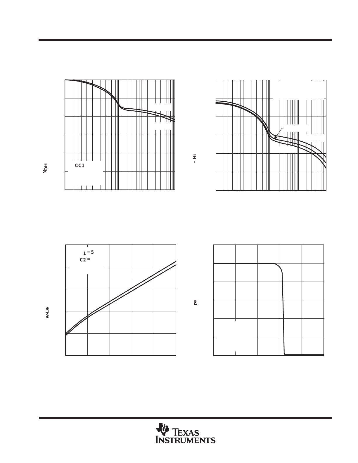
A faster, more ef ficient drive circuit uses an active pull-up as well as an active pull-down output configuration,
referred to as a totem-pole output. The SN75374 driver provides the high-speed totem-pole drive desired in an
application of this type, see Figure 14(a). The resulting faster switching speeds are shown in Figure 14(b).
48 V
5 V
M
4
3–10
7
6
48
TLC555
21
(a)
3
3
5
1/4 SN75374
IRF151
2
OL
1
V
OH
V
VOH – VOl – Gate Voltage – V
0
0 0.5 1 1.5 2 2.5 3
Figure 15. Power MOSFET Drive Using SN75374
POST OFFICE BOX 655303 • DALLAS, TEXAS 75265
t – Time – µs
(b)
Page 11

SN75374
QUADRUPLE MOSFET DRIVER
SLRS028 – SEPTEMBER 1988
APPLICATION INFORMATION
Power MOSFET drivers must be capable of supplying high peak currents to achieve fast switching speeds as
shown by the equation
IPK+
VC
t
r
where C is the capacitive load, and tr is the desired rise time. V is the voltage that the capacitance is charged
to. In the circuit shown in Figure 14(a), V is found by the equation
V = VOH – V
OL
Peak current required to maintain a rise time of 100 ns in the circuit of Figure 14(a) is
*
IPK+
(3*0)4(10
100(10
*
9
)
+
9
)
120 mA
Circuit capacitance can be ignored because it is very small compared to the input capacitance of the IRF151.
With a VCC of 5 V and assuming worst-case conditions, the gate drive voltage is 3 V.
For applications in which the full voltage of V
3 V higher than V
CC2
.
must be supplied to the MOSFET gate, V
CC2
should be at least
CC3
POST OFFICE BOX 655303 • DALLAS, TEXAS 75265
3–11
Page 12

3–12
POST OFFICE BOX 655303 • DALLAS, TEXAS 75265
Page 13

IMPORTANT NOTICE
T exas Instruments and its subsidiaries (TI) reserve the right to make changes to their products or to discontinue
any product or service without notice, and advise customers to obtain the latest version of relevant information
to verify, before placing orders, that information being relied on is current and complete. All products are sold
subject to the terms and conditions of sale supplied at the time of order acknowledgement, including those
pertaining to warranty, patent infringement, and limitation of liability.
TI warrants performance of its semiconductor products to the specifications applicable at the time of sale in
accordance with TI’s standard warranty. Testing and other quality control techniques are utilized to the extent
TI deems necessary to support this warranty . Specific testing of all parameters of each device is not necessarily
performed, except those mandated by government requirements.
CERTAIN APPLICA TIONS USING SEMICONDUCT OR PRODUCTS MAY INVOLVE POTENTIAL RISKS OF
DEATH, PERSONAL INJURY, OR SEVERE PROPERTY OR ENVIRONMENTAL DAMAGE (“CRITICAL
APPLICATIONS”). TI SEMICONDUCTOR PRODUCTS ARE NOT DESIGNED, AUTHORIZED, OR
WARRANTED TO BE SUITABLE FOR USE IN LIFE-SUPPORT DEVICES OR SYSTEMS OR OTHER
CRITICAL APPLICA TIONS. INCLUSION OF TI PRODUCTS IN SUCH APPLICATIONS IS UNDERST OOD TO
BE FULLY AT THE CUSTOMER’S RISK.
In order to minimize risks associated with the customer’s applications, adequate design and operating
safeguards must be provided by the customer to minimize inherent or procedural hazards.
TI assumes no liability for applications assistance or customer product design. TI does not warrant or represent
that any license, either express or implied, is granted under any patent right, copyright, mask work right, or other
intellectual property right of TI covering or relating to any combination, machine, or process in which such
semiconductor products or services might be or are used. TI’s publication of information regarding any third
party’s products or services does not constitute TI’s approval, warranty or endorsement thereof.
Copyright 1998, Texas Instruments Incorporated
 Loading...