

Page 1
SN75207B
DUAL SENSE AMPLIFIER FOR MOS MEMORIES
OR DUAL HIGH-SENSITIVITY LINE RECEIVERS
SLLS096C – JULY 1973 – REVISED MARCH 1997
1
POST OFFICE BOX 655303 • DALLAS, TEXAS 75265
D
Plug-In Replacement for SN75107A and
SN75107B With Improved Characteristics
D
±10-mV Input Sensitivity
D
TTL-Compatible Circuitry
D
Standard Supply Voltages . . . ±5 V
D
Differential Input Common-Mode Voltage
Range of ±3 V
D
Strobe Inputs for Channel Selection
D
Totem-Pole Outputs
D
SN75207B Has Diode-Protected Input Stage
for Power-Off Condition
D
Sense Amplifier for MOS Memories
D
Dual Comparator
D
High-Sensitivity Line Receiver
description
The SN75207B is a terminal-for-terminal replacement for the SN75107B. The improved input sensitivity makes
it more suitable for MOS memory sense amplifiers and can result in faster memory cycles. Improved sensitivity
also makes it more useful in line-receiver applications by allowing use of longer transmission line lengths. The
SN75207B features a TTL-compatible, active-pullup output.
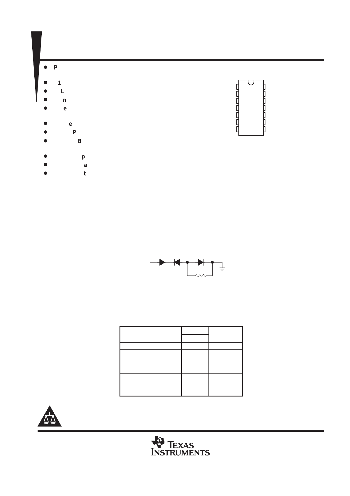
Input protection diodes are in series with the collectors of the differential-input transistors of the SN75207B.
These diodes are useful in certain party-line systems that may have multiple V
CC+
power supplies and may be
operated with some of the V
CC+
supplies turned off. In such a system, if a supply is turned off and allowed to
go to ground, the equivalent input circuit connected to that supply would be as follows:
Input
SN75207B
This would be a problem in specific systems that might have the transmission lines biased to some potential
greater than 1.4 V.
This device is characterized for operation from 0°C to 70°C.
FUNCTION TABLE
DIFFERENTIAL INPUTS
STROBES
OUTPUT
A–B
G S
Y
VID ≥ 10 mV X X H
X L H
–10 mV < VID < 10 mV
L XH
HH Indeterminate
X L H
VID ≤ –10 mV
L XH
HHL
H = high level, L = low level, X = irrelevant
Copyright 1997, Texas Instruments Incorporated
PRODUCTION DATA information is current as of publication date.
Products conform to specifications per the terms of Texas Instruments
standard warranty. Production processing does not necessarily include
testing of all parameters.
Please be aware that an important notice concerning availability, standard warranty, and use in critical applications of
Texas Instruments semiconductor products and disclaimers thereto appears at the end of this data sheet.
1
2
3
4
5
6
7
14
13
12
11
10
9
8
1A
1B
NC
1Y
1G
S
GND
V
CC+
V
CC–
2A
2B
NC
2Y
2G
N PACKAGE
(TOP VIEW)
NC – No internal connection
Page 2
SN75207B
DUAL SENSE AMPLIFIER FOR MOS MEMORIES
OR DUAL HIGH-SENSITIVITY LINE RECEIVERS
SLLS096C – JULY 1973 – REVISED MARCH 1997
2
POST OFFICE BOX 655303 • DALLAS, TEXAS 75265
logic symbol
†
2G
2B
2A
1G
1B
1A
S
8
11
12
5
2
1
6
EN
9
2Y
1Y
4
&
†
This symbol is in accordance with ANSI/IEEE Std 91-1984
and IEC Publication 617-12.
logic diagram (positive logic)
1Y
4
2Y
9
11
2B
12
2A
8
2G
5
1G
2
1B
1A
S
1
6
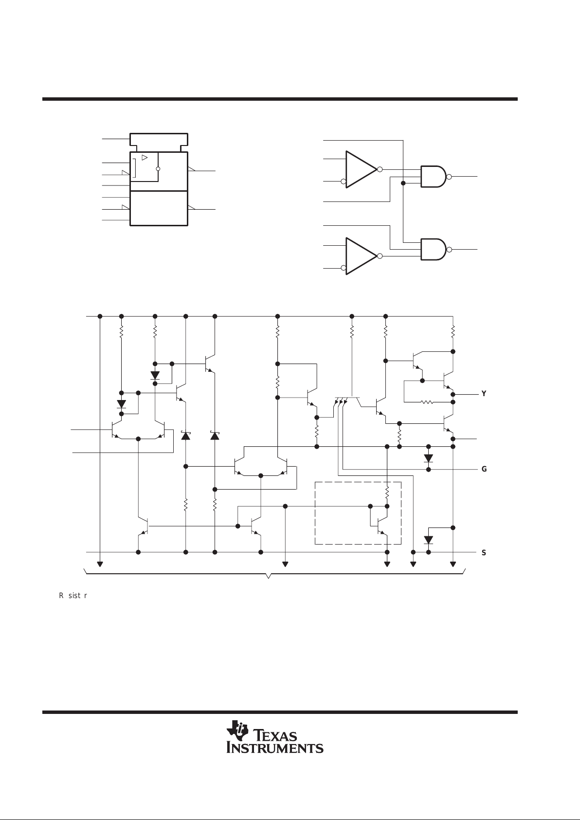
schematic (each receiver)
4 kΩ
4.25 kΩ
6
5, 8
GND
7
4, 9
3 kΩ3 kΩ
800 Ω
1 kΩ
760 Ω
4.8 kΩ
120 Ω
1.6 kΩ
400 Ω1 kΩ1 kΩ
13
V
CC–
2, 11
B
Inputs
A
1, 12
14
V
CC+
To Other Receiver
Y
G
S
Resistor values shown are nominal.
Common
To Both
Receivers
Page 3
SN75207B
DUAL SENSE AMPLIFIER FOR MOS MEMORIES
OR DUAL HIGH-SENSITIVITY LINE RECEIVERS
SLLS096C – JULY 1973 – REVISED MARCH 1997
3
POST OFFICE BOX 655303 • DALLAS, TEXAS 75265
design characteristics
The SN75207B line receivers/sense amplifiers are TTL-compatible, dual circuits intended for use in high-speed,
data-transmission systems or MOS memory systems. They are designed to detect low-level differential signals
in the presence of common-mode noise and variations of temperature and supplies. The dc specifications
reflect worst-case conditions of temperature, supply voltages, and input voltages.
The input common-mode voltage range is ±3 V. This is adequate for application in most systems. In systems
with requirements for greater common-mode voltage range, input attenuators may be used to decrease the
noise to an acceptable level at the receiver-input terminals.
The circuits feature individual strobe inputs for each channel and a strobe input common to both channels for
logic versatility . The strobe inputs are tested to ensure 400 mV of dc noise margin when interfaced with Series
54/74 TTL.
The circuits feature high input impedance and low input currents, which induce very little loading on the
transmission line. This makes these devices especially useful in party-line systems. The excellent input
sensitivity (3 mV typical) is particularly important when data is to be detected at the end of a long transmission
line and the amplitude of the data has deteriorated due to cable losses. The circuits are designed to detect input
signals of 10-mV (or greater) amplitude and convert the polarity of the signal into appropriate TTL-compatible
output logic levels.
absolute maximum ratings over operating free-air temperature range (unless otherwise noted)
†
Supply voltage, V
CC+
(see Note 1) 7 V. . . . . . . . . . . . . . . . . . . . . . . . . . . . . . . . . . . . . . . . . . . . . . . . . . . . . . . . . . . .
Supply voltage, V
CC–
(see Note 1) –7 V. . . . . . . . . . . . . . . . . . . . . . . . . . . . . . . . . . . . . . . . . . . . . . . . . . . . . . . . . . .
Differential input voltage, V
ID
(see Note 2) ±6 V. . . . . . . . . . . . . . . . . . . . . . . . . . . . . . . . . . . . . . . . . . . . . . . . . . . .
Common-mode input voltage, V
IC
(see Note 3) ±5 V. . . . . . . . . . . . . . . . . . . . . . . . . . . . . . . . . . . . . . . . . . . . . . . .
Strobe input voltage 5.5 V. . . . . . . . . . . . . . . . . . . . . . . . . . . . . . . . . . . . . . . . . . . . . . . . . . . . . . . . . . . . . . . . . . . . . . .
Continuous total dissipation See Dissipation Rating Table. . . . . . . . . . . . . . . . . . . . . . . . . . . . . . . . . . . . . . . . . . .
Operating free-air temperature range, T
A
0°C to 70°C. . . . . . . . . . . . . . . . . . . . . . . . . . . . . . . . . . . . . . . . . . . . . .
Storage temperature range, T
stg
–65°C to 150°C. . . . . . . . . . . . . . . . . . . . . . . . . . . . . . . . . . . . . . . . . . . . . . . . . . .
Lead temperature 1,6 mm (1/16 inch) from case for 10 seconds 260°C. . . . . . . . . . . . . . . . . . . . . . . . . . . . . . .
†
Stresses beyond those listed under “absolute maximum ratings” may cause permanent damage to the device. These are stress ratings only, and
functional operation of the device at these or any other conditions beyond those indicated under “recommended operating conditions” is not
implied. Exposure to absolute-maximum-rated conditions for extended periods may affect device reliability.
NOTES: A. All voltage values, except differential voltages, are with respect to GND terminal.
1. Differential input voltage values are at the noninverting (A) terminal with respect to the inverting (B) terminal.
2. Common-mode input voltage is the average of the voltages at the A and B inputs.
DISSIPATION RATING TABLE
PACKAGE
TA ≤ 25°C
POWER RATING
DERATING FACTOR
ABOVE TA = 25°C
TA = 70°C
POWER RATING
N 1050 mW 9.2 mW/°C 636 mW
Page 4

SN75207B
DUAL SENSE AMPLIFIER FOR MOS MEMORIES
OR DUAL HIGH-SENSITIVITY LINE RECEIVERS
SLLS096C – JULY 1973 – REVISED MARCH 1997
4
POST OFFICE BOX 655303 • DALLAS, TEXAS 75265
recommended operating conditions (see Note 4)
MIN NOM MAX UNIT
Supply voltage, V
CC+
4.75 5 5.25 V
Supply voltage, V
CC–
–4.75 –5 –5.25 V
High-level differential input voltage, V
ID(H)
(see Note 5) 0.01 5 V
Low-level differential input voltage, V
ID(L)
–5
†
–0.01 V
Common-mode input voltage, VIC (see Notes 5 and 6)
–3†
3 V
Input voltage, any differential input to ground (see Note 5)
–5†
3 V
High-level input voltage at strobe inputs, V
IH(S)
2 5.5 V
Low-level input voltage at strobe inputs, V
IL(S)
0 0.8 V
Low-level output current, I
OL
–16 mA
Operating free-air temperature, T
A
0 70 °C
†
The algebraic convention, in which the less positive (more negative) limit is designated as minimum, is used in this data sheet for logic voltage
levels only.
NOTES: B. When using only one channel of the line receiver, the strobe G of the unused channel should be grounded and at least one of the
differential inputs of the unused receiver should be terminated at some voltage between –3 V and 3 V.
3. The recommended combinations of input voltages fall within the shaded area of the figure shown.
4. The common-mode voltage may be as low as –4 V provided that the more positive of the two inputs is not more negative than –3 V .
321– 1– 2– 3– 4
3
2
1
0
– 1
– 2
– 3
– 4
– 5
Inputs – B-to-Ground Voltage – V
Inputs – A-to-Ground Voltage – V
– 5 0
Page 5

SN75207B
DUAL SENSE AMPLIFIER FOR MOS MEMORIES
OR DUAL HIGH-SENSITIVITY LINE RECEIVERS
SLLS096C – JULY 1973 – REVISED MARCH 1997
5
POST OFFICE BOX 655303 • DALLAS, TEXAS 75265
electrical characteristics over recommended free-air temperature range (unless otherwise noted)
PARAMETER TEST CONDITIONS MIN TYP†MAX UNIT
I
IH
High-level input current V
CC±
= ± 5.25 V VID = –5 V 30 75 µA
I
IL
Low-level input current V
CC±
= ± 5.25 V VID = 5 V –10 µA
High-level input current
V
CC±
= ± 5.25 V , V
IH(S)
= 2.4 V 40 µA
I
IH
g
into 1G or 2G
V
CC±
= ± 5.25 V ,
V
IH(S)
= ± 5.25 V 1 mA
Low-level input current
I
IL
into 1G or 2G
V
CC±
= ± 5.25 V,
V
IL(S)
= 0.4
V
–1.
6
mA
p
V
CC±
= ± 5.25 V , V
IH(S)
= 2.4 V 80 µA
IIHHigh-level input current into S
V
CC±
= ± 5.25 V , V
IH(S)
= ± 5.25 V 2 mA
I
IL
Low-level input current into S V
CC±
= ± 5.25 V , V
IL(S)
= 0.4 V –3.2 mA
p
V
= ± 4.75 V , V
= 0.8 V, V
= 10 mV,
VOHHigh-level output voltage
CC±
,
IOH = –400 µA,
IL(S)
,
VIC = –3 V to 3 V
ID(H)
,
2.4
V
p
V
= ± 4.75 V , V
= 2 V, V
= –10 mV ,
VOLLow-level output voltage
CC±
,
IOL = 16 mA,
IH(S)
,
VIC = –3 V to 3 V
ID(L)
,
0.4
V
I
OH
High-level output current V
CC±
= ± 4.75 V , VOH = ±5.25 V 400 µA
I
OS
Short-circuit output current
‡
V
CC±
= ± 5.25 V –18 –70 mA
I
CC+
Supply current from V
CC+
V
CC±
= ± 5.25 V , TA = 25°C, Outputs high 18 30 mA
I
CC–
Supply current from V
CC–
V
CC±
= ± 5.25 V , TA = 25°C, Outputs high –8.4 –15 mA
†
All typical values are at V
CC+
= 5 V, V
CC–
= –5 V, TA = 25°C.
‡
Not more than one output should be shorted at a time.
switching characteristics, V
CC+
= 5 V, V
CC–
= –5 V, TA = 25°C
PARAMETER
TEST
CONDITIONS
MIN MAX UNIT
t
PLH(D)
Propagation delay time, low- to high-level output, from differential inputs A and B
35 ns
t
PHL(D)
Propagation delay time, high- to low-level output, from differential inputs A and B
RL = 470 Ω, CL = 50 pF,
20 ns
t
PLH(S)
Propagation delay time, low- to high-level output, from strobe
input G or S
L
See Figure 1
L
17 ns
t
PHL(S)
Propagation delay time, high- to low-level output, from strobe
input G or S
17 ns
Page 6

SN75207B
DUAL SENSE AMPLIFIER FOR MOS MEMORIES
OR DUAL HIGH-SENSITIVITY LINE RECEIVERS
SLLS096C – JULY 1973 – REVISED MARCH 1997
6
POST OFFICE BOX 655303 • DALLAS, TEXAS 75265
PARAMETER MEASUREMENT INFORMATION
t
w1
50 Ω
VOLTAGE WAVEFORMS
V
OL
V
OH
0 V
3 V
1.5 V1.5 V
t
w2
1.5 V1.5 V
t
PHL(S)
t
PLH(S)
1.5 V
t
PLH(D)
1.5 V
t
PHL(D)
Y
V
OL
V
OH
G or S
3 V
40 mV
B
10 mV10 mV
0 V
40 mV
TEST CIRCUIT
Pulse
Generator
(see Note A)
Strobe
Input
(see Note B)
50 Ω
V
CC+
2GS1G
See Note D
470 Ω
Output
1Y
2Y
V
CC–
2B
2A
1B
1A
100 mV
V
ref
Differential
Input
CL = 50 pF
(see Note C)
Pulse
Generator
(see Note A)
NOTES: A. The pulse generators have the following characteristics: ZO = 50 Ω, tr ≤ 5 ns, tf ≤ 5 ns, tw1 = 500 ns with PRR = 1 MHz, tw2 = 1 µs
with PRR = 500 kHz.
B. Strobe input pulse is applied to Strobe 1G when inputs 1A–1B are being tested, to Strobe S when inputs 1A–1B or 2A–2B are being
tested, and to Strobe 2G when inputs 2A–2B are being tested.
C. CL includes probe and jig capacitance.
D. All diodes are 1N916.
Figure 1. Test Circuit and Voltage Waveforms
Page 7

SN75207B
DUAL SENSE AMPLIFIER FOR MOS MEMORIES
OR DUAL HIGH-SENSITIVITY LINE RECEIVERS
SLLS096C – JULY 1973 – REVISED MARCH 1997
7
POST OFFICE BOX 655303 • DALLAS, TEXAS 75265
APPLICATION INFORMATION
Input
From
TTL
SN75361A
or
SN75452B
MOS Memory
V
ref
Adjustment
100 Ω
100 Ω
’207B
Drive Memory Sense
Output
to TTL
Strobes
To
Dummy
Line
Figure 2. MOS Memory Sense Amplifier
Y
Receiver 4
Transmission Line Having
Characteristics Impedance Z
O
Receiver 2
YY
Strobes
Receiver 1
R
T
R
T
Location 2
Location 4
Driver 4
D
C
B
A
Location 3
Driver 3
A
B
C
D
Location 1
Inhibit
Data Input
D
C
B
A
Driver 1
R
T
R
T
Strobes
Strobes
Receivers are SN75207B; drivers are SN55109A, SN55110A, SN75110A, or SN75112.
Figure 3. Data-Bus or Parity-Line System
PRECAUTIONS: When only one receiver in a package is being used, at least one of the differential inputs of the
unused receiver should be terminated at some voltage between –3 V and 3 V, preferably at GND. Failure to do so
will cause improper operation of the unit being used because of common bias circuitry for the current sources of the
two receivers. Strobe G of the unused channel should be grounded.
Page 8

IMPORTANT NOTICE
T exas Instruments and its subsidiaries (TI) reserve the right to make changes to their products or to discontinue
any product or service without notice, and advise customers to obtain the latest version of relevant information
to verify, before placing orders, that information being relied on is current and complete. All products are sold
subject to the terms and conditions of sale supplied at the time of order acknowledgement, including those
pertaining to warranty, patent infringement, and limitation of liability.
TI warrants performance of its semiconductor products to the specifications applicable at the time of sale in
accordance with TI’s standard warranty. Testing and other quality control techniques are utilized to the extent
TI deems necessary to support this warranty. Specific testing of all parameters of each device is not necessarily
performed, except those mandated by government requirements.
CERT AIN APPLICATIONS USING SEMICONDUCTOR PRODUCTS MAY INVOLVE POTENTIAL RISKS OF
DEATH, PERSONAL INJURY, OR SEVERE PROPERTY OR ENVIRONMENTAL DAMAGE (“CRITICAL
APPLICATIONS”). TI SEMICONDUCTOR PRODUCTS ARE NOT DESIGNED, AUTHORIZED, OR
WARRANTED TO BE SUITABLE FOR USE IN LIFE-SUPPORT DEVICES OR SYSTEMS OR OTHER
CRITICAL APPLICATIONS. INCLUSION OF TI PRODUCTS IN SUCH APPLICA TIONS IS UNDERST OOD TO
BE FULLY AT THE CUSTOMER’S RISK.
In order to minimize risks associated with the customer’s applications, adequate design and operating
safeguards must be provided by the customer to minimize inherent or procedural hazards.
TI assumes no liability for applications assistance or customer product design. TI does not warrant or represent
that any license, either express or implied, is granted under any patent right, copyright, mask work right, or other
intellectual property right of TI covering or relating to any combination, machine, or process in which such
semiconductor products or services might be or are used. TI’s publication of information regarding any third
party’s products or services does not constitute TI’s approval, warranty or endorsement thereof.
Copyright 1998, Texas Instruments Incorporated
 Loading...