

SN75196
MULTIPLE RS-232 DRIVERS AND RECEIVERS
SLLS188B – MAY 1995 – REVISED APRIL 1998
1
POST OFFICE BOX 655303 • DALLAS, TEXAS 75265
D
Single Chip With Easy Interface Between
UART and Serial-Port Connector of an
External Modem or Other Computer
Peripheral
D
Five Drivers and Three Receivers Meet or
Exceed the Requirements of TIA/EIA-232-F
and ITU Recommendation V.28
D
Designed to Support Data Rates up to
120 kbit/s
D
ESD Protection Meets Or Exceeds 10 kV on
RS-232 Pins and 5 kV on All Other Pins
(Human-Body Model)
D
Complement to the SN75185
D
Pin-to-Pin Replacement for the Goldstar
GD75323
D
Functional Replacement for the MC145405
description
The SN75196 combines five drivers and three receivers from the trade-standard SN75188 and SN75189
bipolar quadruple drivers and receivers, respectively . The flow-through design of the SN75196 decreases the
part count, reduces the board space required, and allows easy interconnection of the UART and serial-port
connector. The all-bipolar circuits and processing of the SN75196 provide a rugged, low-cost solution for this
function.
The SN75196 complies with the requirements of TIA/EIA-232-F and ITU (formerly CCITT) V.28 standards.
These standards are for data interchange between a host computer and peripheral at signal rates of up to
20 kbit/s. The switching speeds of the SN75196 are fast enough to support rates of up to 120 kbit/s with lower
capacitive loads (shorter cables). Interoperability at the higher signaling rates cannot be assured unless the
designer has design control of the cable and the interface circuits at both ends. For interoperability at signaling
rates of up to 120 kbit/s, use of TIA/EIA-423-B (ITU V.10) and TIA/EIA-422-B (ITU V.11) standards are
recommended.
The SN75196 is characterized for operation over a temperature range of 0°C to 70°C.
Copyright 1998, Texas Instruments Incorporated
PRODUCTION DATA information is current as of publication date.
Products conform to specifications per the terms of Texas Instruments
standard warranty. Production processing does not necessarily include
testing of all parameters.
Please be aware that an important notice concerning availability, standard warranty, and use in critical applications of
Texas Instruments semiconductor products and disclaimers thereto appears at the end of this data sheet.
1
2
3
4
5
6
7
8
9
10
20
19
18
17
16
15
14
13
12
11
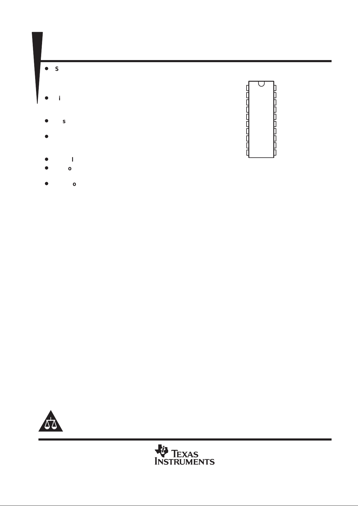
V
CC
1DA
2DA
3DA
1RY
2RY
4DA
3RY
5DA
GND
V
DD
1DY
2DY
3DY
1RA
2RA
4DY
3RA
5DY
V
SS
DW OR N PACKAGE
(TOP VIEW)
SN75196
MULTIPLE RS-232 DRIVERS AND RECEIVERS
SLLS188B – MAY 1995 – REVISED APRIL 1998
2
POST OFFICE BOX 655303 • DALLAS, TEXAS 75265
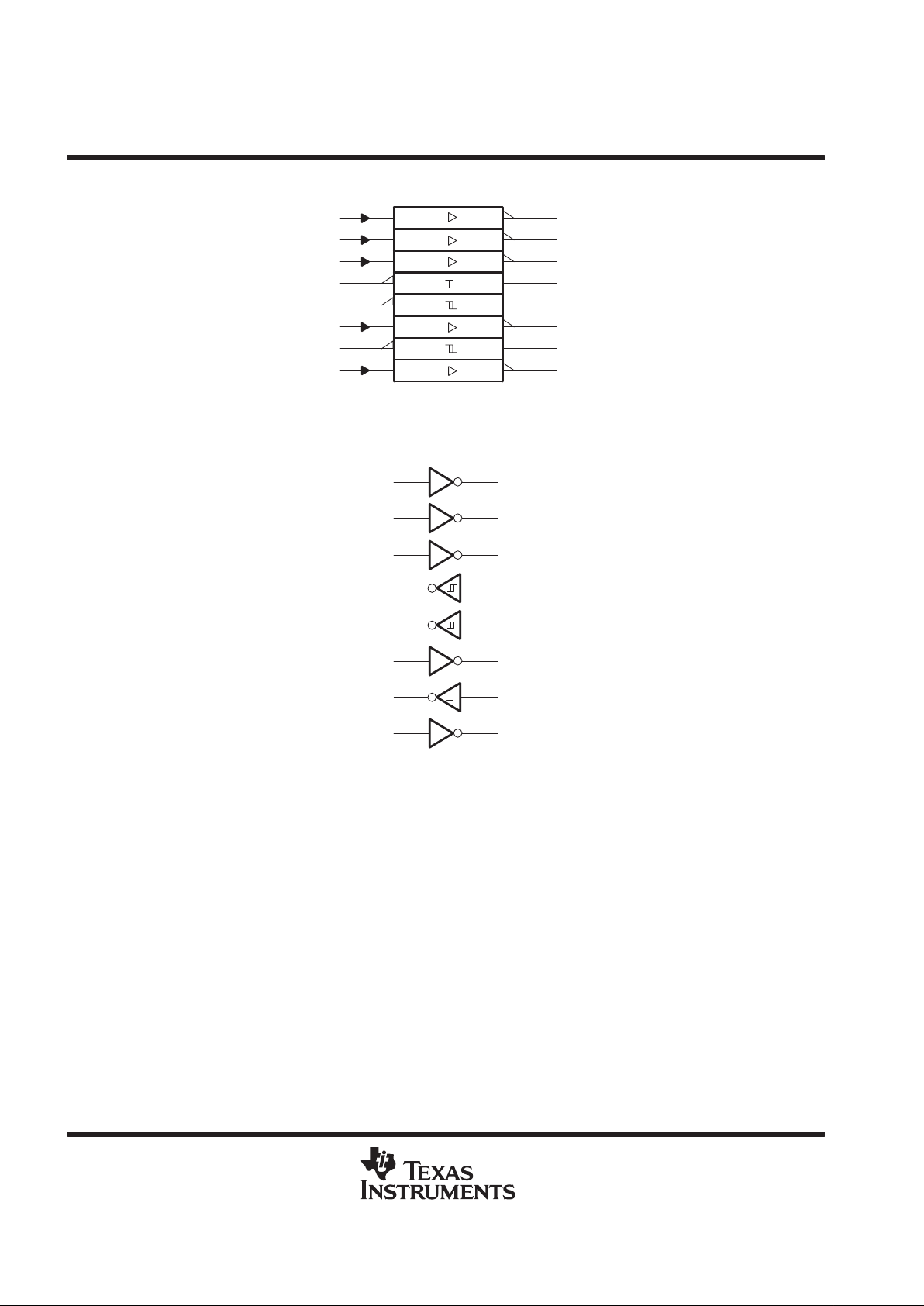
logic symbol
†
†
This symbol is in accordance with ANSI/IEEE Std 91-1984 and IEC Publication 617-12.
9
8
7
6
5
4
3
2
5DY
3RA
4DY
2RA
1RA
3DY
2DY
1DY
5DA
3RY
4DA
2RY
1RY
3DA
2DA
1DA
12
13
14
15
16
17
18
19
logic diagram (positive logic)
1DY1DA
2DY2DA
3DY3DA
1RA1RY
2RA2RY
4DY4DA
3RA3RY
5DY5DA
2
3
4
5
6
7
8
9
19
18
12
13
14
15
16
17
SN75196
MULTIPLE RS-232 DRIVERS AND RECEIVERS
SLLS188B – MAY 1995 – REVISED APRIL 1998
3
POST OFFICE BOX 655303 • DALLAS, TEXAS 75265
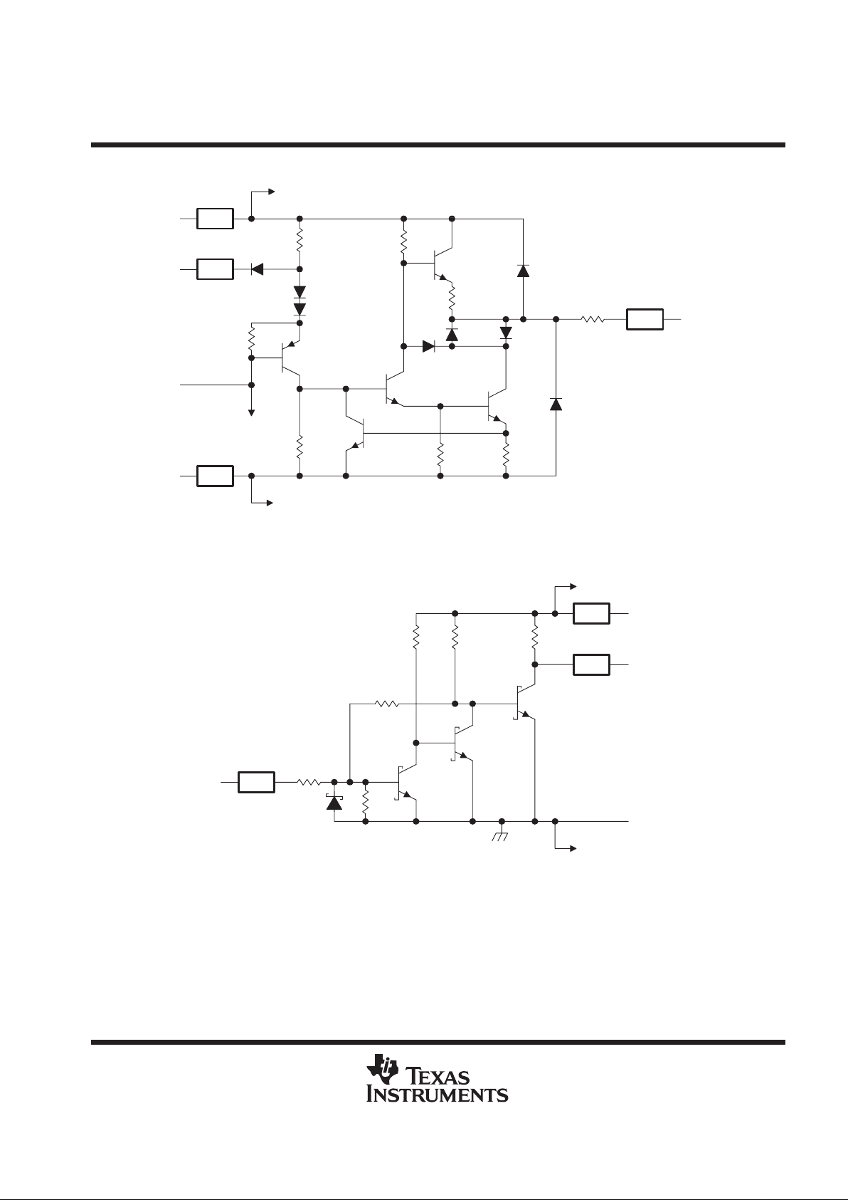
schematic of each driver
DYx Output
320 Ω
68.5 Ω3.3 kΩ
10.4 kΩ
To Other Drivers
V
SS
To Other
Drivers
GND
4.2 kΩ
Input DAx
V
DD
75.8 Ω
9.4 kΩ11.6 kΩ
To Other Drivers
Resistor values shown are nominal.
ESD
ESD
ESD
ESD
schematic of each receiver
Input RAx
10 kΩ
3.8 kΩ
9 kΩ 5 kΩ
1.66 kΩ
GND
RYx Output
V
CC
ESD
To Other Receivers
Resistor values shown are nominal.
2 kΩ
ESD
To Other Receivers
ESD
SN75196
MULTIPLE RS-232 DRIVERS AND RECEIVERS
SLLS188B – MAY 1995 – REVISED APRIL 1998
4
POST OFFICE BOX 655303 • DALLAS, TEXAS 75265
absolute maximum ratings over operating free-air temperature (unless otherwise noted)
†
Supply voltage, V
CC
(see Note 1) 10 V. . . . . . . . . . . . . . . . . . . . . . . . . . . . . . . . . . . . . . . . . . . . . . . . . . . . . . . . . . . .
Supply voltage, V
DD
(see Note 1) 15 V. . . . . . . . . . . . . . . . . . . . . . . . . . . . . . . . . . . . . . . . . . . . . . . . . . . . . . . . . . . .
Supply voltage, V
SS
(see Note 1) –15 V. . . . . . . . . . . . . . . . . . . . . . . . . . . . . . . . . . . . . . . . . . . . . . . . . . . . . . . . . . .
Input voltage range, V
I
: Driver –15 V to 7 V. . . . . . . . . . . . . . . . . . . . . . . . . . . . . . . . . . . . . . . . . . . . . . . . . . . . . . . .
Receiver –30 V to 30 V. . . . . . . . . . . . . . . . . . . . . . . . . . . . . . . . . . . . . . . . . . . . . . . . . . .
Output voltage range, V
O
(Driver) – 15 V to 15 V. . . . . . . . . . . . . . . . . . . . . . . . . . . . . . . . . . . . . . . . . . . . . . . . . . .
Low-level output current, I
OL
(Receiver) 20 mA. . . . . . . . . . . . . . . . . . . . . . . . . . . . . . . . . . . . . . . . . . . . . . . . . . . .
Continuous total power dissipation See Dissipation Rating Table. . . . . . . . . . . . . . . . . . . . . . . . . . . . . . . . . . . . .
Electrostatic discharge: DY and RA to GND (see Note 2) Class 3, A: 10 kV, B: 500 V. . . . . . . . . . . . . . . . . .
All pins (see Note 2) Class 3, A: 5 kV, B: 300 V. . . . . . . . . . . . . . . . . . . . . . . . . . . . . . .
Storage temperature range, T
stg
–65°C to 150°C. . . . . . . . . . . . . . . . . . . . . . . . . . . . . . . . . . . . . . . . . . . . . . . . . .
Lead temperature 1,6 mm (1/16 inch) from case for 10 seconds 260°C. . . . . . . . . . . . . . . . . . . . . . . . . . . . . . .
†
Stresses beyond those listed under “absolute maximum ratings” may cause permanent damage to the device. These are stress ratings only, and
functional operation of the device at these or any other conditions beyond those indicated under “recommended operating conditions” is not
implied. Exposure to absolute-maximum-rated conditions for extended periods may affect device reliability.
NOTES: 1. All voltages are with respect to the network ground terminal.
2. Per MIL-PRF-38535, Method 3015.7
DISSIPATION RATING TABLE
PACKAGE
TA ≤ 25°C
POWER RATING
DERATING FACTOR
‡
ABOVE TA = 25°C
TA = 70°C
POWER RATING
DW 1 125 mW 9.0 mW/°C 720 mW
N 1150 mW 9.2 mW/°C 736 mW
‡
This is the inverse of the traditional junction-to-case thermal resistance (R
θJA
).
recommended operating conditions
MIN NOM MAX UNIT
Supply voltage, V
DD
7.5 9 13.5 V
Supply voltage, V
SS
–7.5 –9 –13.5 V
Supply voltage, V
CC
4.5 5 5.5 V
High-level input voltage, V
IH
Driver 1.9 V
Low-level input voltage, V
IL
Driver 0.8 V
p
Driver –6
High-level output current, I
OH
Receiver –0.5
mA
p
Driver 6
High-level output current, I
OL
Receiver 16
mA
Operating free-air temperature,T
A
0 70 °C

SN75196
MULTIPLE RS-232 DRIVERS AND RECEIVERS
SLLS188B – MAY 1995 – REVISED APRIL 1998
5
POST OFFICE BOX 655303 • DALLAS, TEXAS 75265
supply currents over operating free-air temperature range
PARAMETER TEST CONDITIONS MIN MAX UNIT
p
VDD = 9 V, VSS = –9 V 25
pp
All inputs at 1.9 V
,
No load
VDD = 12 V, VSS = –12 V 32
IDDSupply current from V
DD
p
VDD = 9 V, VSS = –9 V 7.5
mA
All inputs at 0.8 V
,
No load
VDD = 12 V, VSS = –12 V 9.5
p
VDD = 9 V, VSS = –9 V –25
pp
All inputs at 1.9 V
,
No load
VDD = 12 V, VSS = –12 V –32
ISSSupply current from V
SS
p
VDD = 9 V, VSS = –9 V –5.3
mA
All inputs at 0.8 V
,
No load
VDD = 12 V, VSS = –12 V –5.3
I
CC
Supply current from V
CC
VCC = 5 V, All inputs at 5 V, No load 20 mA
DRIVER SECTION
electrical characteristics over operating free-air temperature range, V
DD
= 9 V , VSS = –9 V , VCC= 5 V,
(unless otherwise noted)
PARAMETER TEST CONDITIONS MIN TYP MAX UNIT
V
OH
High-level output voltage VIL = 0.8 V, RL = 3 kΩ, See Figure 1 6 7.5 V
V
OL
Low-level output voltage (see Note 3) VIH = 1.9 V, RL = 3 kΩ, See Figure 1 –7.5 –6 V
I
IH
High-level input current VI = 5 V, See Figure 2 10 µA
I
IL
Low-level input current VI = 0, See Figure 2 –1.6 mA
I
OS(H)
High-level short-circuit output current
(see Note 4)
VIL = 0.8 V, VO = 0, See Figure 1 –4.5 –9 –19.5 mA
I
OS(L)
Low-level short-circuit output current
(see Note 4)
VIH = 2 V, VO = 0, See Figure 1 4.5 9 19.5 mA
r
o
Output resistance (see Note 5) VCC = VDD = VSS = 0, VO = –2 V to 2 V 300 Ω
NOTES: 3. The algebraic convention, where the more positive (less negative) limit is designated as maximum, is used in this data sheet for logic
levels only, e.g., if –10 V is a maximum, the typical value is a more negative voltage.
4. Output short-circuit conditions must maintain the total power dissipation below absolute maximum ratings.
5. Test conditions are those specified by TIA/EIA-232-F and as listed above.
switching characteristics, VDD = 12 V, VSS = –12 V, VCC = 5 V ±10%, TA = 25°C
PARAMETER TEST CONDITIONS MIN TYP MAX UNIT
t
PLH
Propagation delay time,
low- to high-level output
RL = 3 kΩ to 7 kΩ, CL = 15 pF, See Figure 3 315 500 ns
t
PHL
Propagation delay time,
high- to low-level output
RL = 3 kΩ to 7 kΩ, CL = 15 pF, See Figure 3 75 175 ns
Transition time,
p
CL = 15 pF, See Figure 3 60 100 ns
t
TLH
l
ow- to high-level outpu
t
(see Note 6)
R
L
= 3 kΩ to 7
kΩ
CL = 2500 pF, See Figure 3 and Note 6 1.7 2.5 µs
Transition time,
p
CL = 15 pF, See Figure 3 40 75 ns
t
THL
high- to low-level out ut
(see Note 7)
R
L
= 3 kΩ to 7
kΩ
CL = 2500 pF, See Figure 3 and Note 7 1.5 2.5 µs
NOTES: 6. Measured between –3-V and 3-V points of the output waveform (TIA/EIA-232-F conditions), all unused inputs are tied either high
or low.
7. Measured between 3-V and –3-V points of the output waveform (TIA/EIA-232-F conditions), all unused inputs are tied either high
or low.

SN75196
MULTIPLE RS-232 DRIVERS AND RECEIVERS
SLLS188B – MAY 1995 – REVISED APRIL 1998
6
POST OFFICE BOX 655303 • DALLAS, TEXAS 75265
RECEIVER SECTION
electrical characteristics over recommended operating conditions (unless otherwise noted)
PARAMETER TEST CONDITIONS MIN
TYP
Ĕ
MAX UNIT
p
TA = 25°C 1.75 1.9 2.3
V
IT+
Positive-going input threshold voltage
See Figure 5
TA = 0°C to 70 °C 1.55 2.3
V
V
IT–
Negative-going input threshold voltage See Figure 5 0.75 0.97 1.25 V
V
hys
Input hysteresis (V
IT+
– V
IT–
) See Figure 5 0.5 V
p
VIH = 0.75 V 2.6 4 5
VOHHigh-level output voltage
I
OH
= –
0.5 mA
,
See Figure 5
Inputs open 2.6
V
V
OL
Low-level input voltage IOL = 10 mA, VI = 3 V, See Figure 5 0.2 0.45 V
p
VI = 25 V 3.6 8.3
IIHHigh-level input current
VI = 3 V 0.43
mA
p
VI = –25 V –3.6 –8.3
IILLow-level input current
VI = –3 V –0.43
mA
I
OS
Short-circuit output current See Figure 4 –3.4 –12 mA
†
All typical values are at TA = 25°C, VCC = 5 V, VDD = 9 V, and VSS = –9 V .
switching characteristics, VCC = 5 V, VDD = 12 V, VSS = –12 V, TA = 25°C
PARAMETER TEST CONDITIONS MIN TYP MAX UNIT
t
PLH
Propagation delay time, low- to high-level output CL = 50 pF, RL = 5 kΩ, See Figure 6 107 500 ns
t
PHL
Propagation delay time, high- to low-level output CL = 50 pF, RL = 5 kΩ, See Figure 6 42 150 ns
t
TLH
Transition time, low- to high-level output CL = 50 pF, RL = 5 kΩ, See Figure 6 175 525 ns
t
THL
Transition time, high- to low-level output CL = 50 pF, RL = 5 kΩ, See Figure 6 16 60 ns

SN75196
MULTIPLE RS-232 DRIVERS AND RECEIVERS
SLLS188B – MAY 1995 – REVISED APRIL 1998
7
POST OFFICE BOX 655303 • DALLAS, TEXAS 75265
PARAMETER MEASUREMENT INFORMATION
I
OS(L)
–I
OS(H)
V
SS
V
DD
V
CC
V
I
V
O
VDD or GND
VSS or GND
RL = 3 kΩ
Figure 1. Driver Test Circuit for VOH, VOL, I
OS(H)
, and I
OS(L)
–I
IL
I
IH
V
SS
V
DD
V
CC
V
I
V
I
Figure 2. Driver Test Circuit for IIH and I
IL
Pulse
Generator
See Note A
C
L
(see Note B)
R
L
3 V
0 V
1.5 V
1.5 V
Input
t
PHL
t
PLH
90%
50%
10%
50%
10%
90%
t
THL
t
TLH
V
OH
V
OL
TEST CIRCUIT VOLTAGE W AVEFORMS
Input
Output
V
SS
V
CC
V
DD
V
O
NOTES: A. The pulse generator has the following characteristics: tw = 25 µs, PRR = 20 kHz, ZO = 50 Ω, tr = tf < 50 ns.
B. CL includes probe and jig capacitance.
Figure 3. Driver Test Circuit and Voltage Waveforms

SN75196
MULTIPLE RS-232 DRIVERS AND RECEIVERS
SLLS188B – MAY 1995 – REVISED APRIL 1998
8
POST OFFICE BOX 655303 • DALLAS, TEXAS 75265
PARAMETER MEASUREMENT INFORMATION
V
I
V
DD
V
CC
V
SS
–I
OS
Figure 4. Receiver Test Circuit for I
OS
VIT, V
I
V
DD
V
CC
V
SS
I
OL
V
OH
–I
OH
V
OL
Figure 5. Receiver Test Circuit for VIT, VOH, and V
OL
5 V
–5
V
50%
50%
Input
t
PHL
t
PLH
90%
50%
10%
50%
10%
90%
t
THL
t
TLH
V
O
H
V
O
L
VOLTAGE WAVEFORMS
Output
NOTES: A. The pulse generator has the following characteristics: tw = 25 µs, PRR = 20 kHz, ZO = 50 Ω, tr = tf < 50 ns.
B. CL includes probe and jig capacitance.
Pulse
Generator
See Note A
C
L
(see Note B)
R
L
TEST CIRCUIT
Input
V
SS
V
CC
V
DD
V
O
Figure 6. Receiver Propagation and Transition Times

SN75196
MULTIPLE RS-232 DRIVERS AND RECEIVERS
SLLS188B – MAY 1995 – REVISED APRIL 1998
9
POST OFFICE BOX 655303 • DALLAS, TEXAS 75265
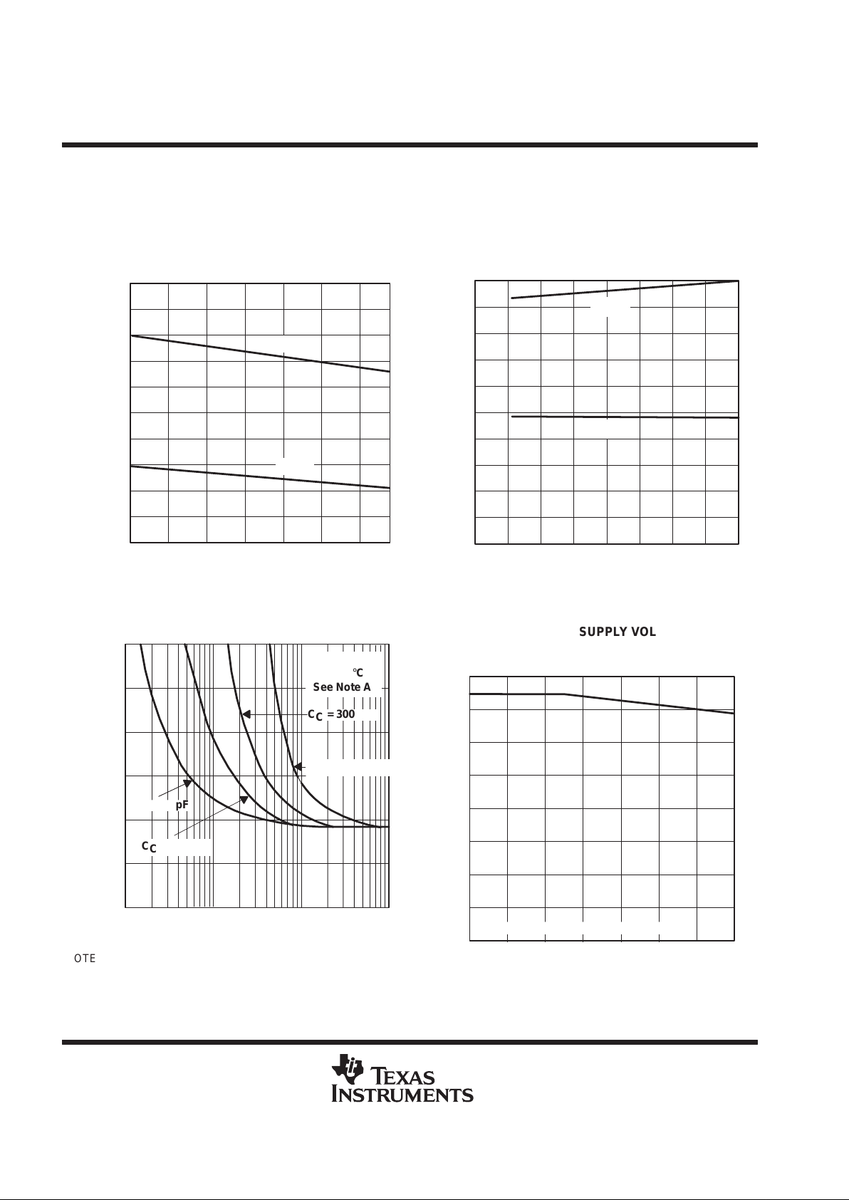
TYPICAL CHARACTERISTICS
DRIVER SECTION
1.81.61.41.20.60.40.2
Figure 7
V
VOLTAGE TRANSFER CHARACTERISTICS
VDD = 6 V, VSS = –6 V
9
6
3
0
–3
–6
–9
0.8
–12
12
VI – Input Voltage – V
0
VDD = 12 V, VSS = –12 V
VDD = 9 V, VSS = –9 V
RL = 3 kΩ
TA = 25°C
12
O
– Output Voltage – V
Figure 8
OUTPUT CURRENT
vs
OUTPUT VOLTAGE
16
12
8
4
0
–4
–8
–12
–16
12840–4–8–12
–20
16
20
VO – Output Voltage – V
–16
VOL(VI = 1.9 V)
3-kΩ
Load Line
VDD = 9 V
VSS = –9 V
TA = 25°C
I
O
– Output Current – mA
VOH(VI = 0.8 V)
Figure 9
SHORT-CIRCUIT OUTPUT CURRENT
vs
FREE-AIR TEMPERATURE
70605040302010
9
6
3
0
–3
–6
–9
–12
12
TA – Free-Air Temperature – °C
0
VDD = 9 V
VSS = –9 V
VO = 0
I
OS(H)
(VI = 0.8 V)
I
OS(L)
(VI = 1.9 V)
I
OS
– Short-Circuit Output Current – mA
Figure 10
SLEW RATE
vs
LOAD CAPACITANCE
VDD = 9 V
VSS = –9 V
RL = 3 kΩ
TA = 25°C
100
10
1000100
1
10000
1000
CL – Load Capacitance – pF
10
SR – Slew Rate – V/µ s
SN75196
MULTIPLE RS-232 DRIVERS AND RECEIVERS
SLLS188B – MAY 1995 – REVISED APRIL 1998
10
POST OFFICE BOX 655303 • DALLAS, TEXAS 75265
TYPICAL CHARACTERISTICS
RECEIVER SECTION
Figure 11
INPUT THRESHOLD VOLTAGE
vs
FREE-AIR TEMPERATURE
2.2
2
1.8
1.6
1.4
1.2
0.8
0.6
0.4
2.4
TA – Free-Air Temperature – °C
V
IT–
V
IT+
706050403020100
1
– Input Threshold Voltage – VV
IT
Figure 12
INPUT THRESHOLD VOLTAGE
vs
SUPPLY VOLTAGE
1.8
1.6
1.4
1.2
1
0.8
0.6
0.4
0.2
9876543
0
10
2
VCC – Supply Voltage – V
2
V
IT–
V
IT+
– Input Threshold Voltage – VV
IT
Figure 13
Amplitude – V
NOISE REJECTION
CC = 300 pF
10
tw – Pulse Duration – ns
6
10000
0
1
2
3
4
5
100 400 1000 4000
CC = 12 pF
CC = 100 pF
NOTE A: This figure shows the maximum amplitude of a
positive-going pulse that, starting from 0 V, does not cause
a change of the output level.
VCC = 5 V
TA = 25°C
See Note A
CC = 500 pF
Figure 14
MAXIMUM SUPPLY VOLTAGE
vs
FREE-AIR TEMPERATURE
14
12
10
8
6
4
2
70605040302010
0
16
TA – Free-Air Temperature – °C
0
– Maximum Supply Voltage – VV
DD
RL ≥ 3 kΩ (from each output to GND)
SN75196
MULTIPLE RS-232 DRIVERS AND RECEIVERS
SLLS188B – MAY 1995 – REVISED APRIL 1998
11
POST OFFICE BOX 655303 • DALLAS, TEXAS 75265
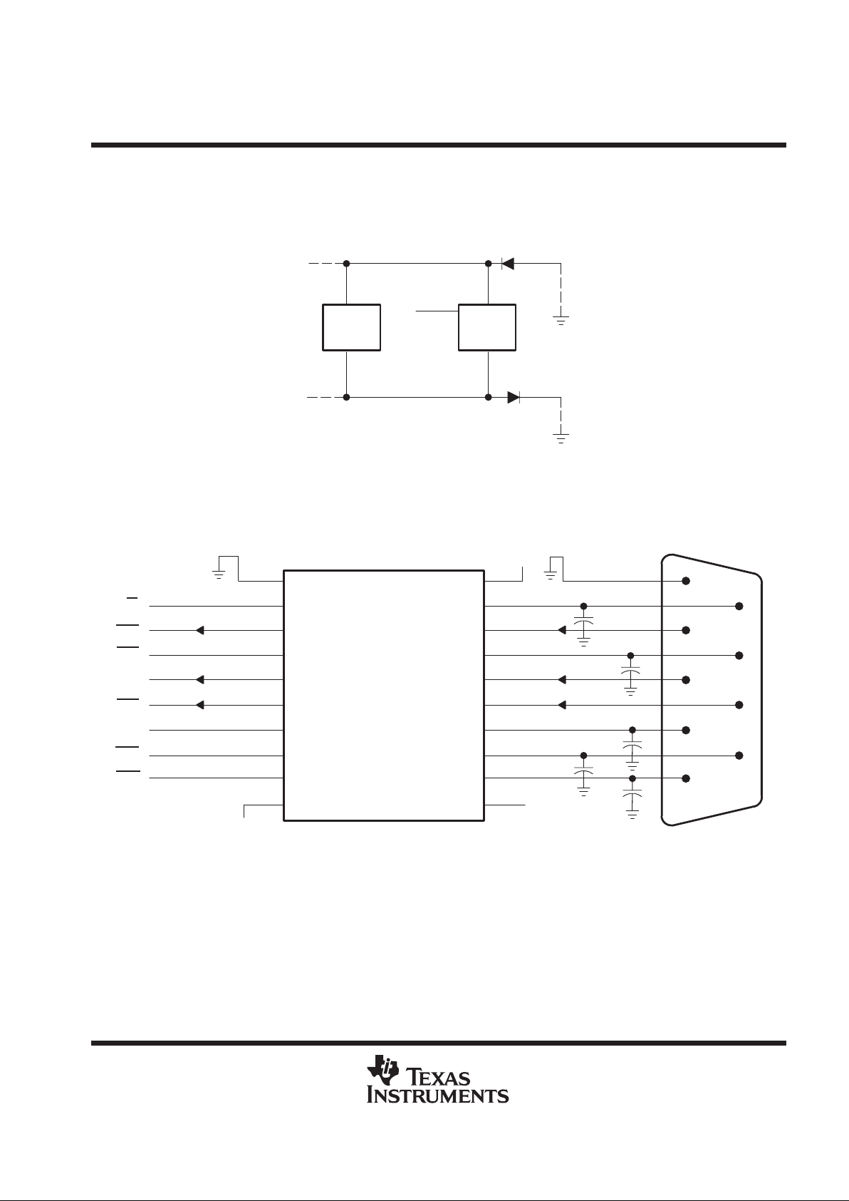
APPLICATION INFORMATION
Diodes placed in series with the V
DD
and VSS terminals protect the SN75196 in the fault condition when the device
outputs are shorted to V
DD
or VSS and the power supplies are at low and provide low-impedance paths to ground
(see Figure 15).
V
DD
V
SS
±15 V
Output
V
DD
V
SS
SN75196 SN75196
Figure 15. Power-Supply Protection to Meet Power-Off Fault Conditions of TIA/EIA-232-F
SN75196
5 V
TL16C450
ACE
1
5
6
9
12 V
–12 V
TIA/EIA-232-F
DB9S
Connector
C2
†
C5
†
†
See Figure 10 to select the correct values for the loading capacitors (C1, C2, C3, C4, and C5), which may be required to meet the RS-232
maximum slew-rate requirement of 30 V/µs. The value of the loading capacitors required depends upon the line length and desired slew rate,
but is typically 330 pF.
NOTE A: To use the receivers only, VDD and VSS must both be powered or tied to ground.
C4
†
C3
†
C1
†
RI
DTR
CTS
SO
RTS
SI
DSR
DCD
43
37
40
13
36
11
41
42
10
9
8
7
6
5
4
3
2
1
GND
5DA
3RY
4DA
2RY
1RY
2DA
1DA
V
CC
3DA
V
SS
5DY
3RA
4DY
2RA
1RA
2DY
1DY
V
DD
3DY
11
12
13
14
15
16
17
18
19
20
RI
DTR
CTS
TX
RTS
RX
DSR
DCD
Figure 16. Typical TIA/EIA-232-F Connection

IMPORTANT NOTICE
T exas Instruments and its subsidiaries (TI) reserve the right to make changes to their products or to discontinue
any product or service without notice, and advise customers to obtain the latest version of relevant information
to verify, before placing orders, that information being relied on is current and complete. All products are sold
subject to the terms and conditions of sale supplied at the time of order acknowledgement, including those
pertaining to warranty, patent infringement, and limitation of liability.
TI warrants performance of its semiconductor products to the specifications applicable at the time of sale in
accordance with TI’s standard warranty. Testing and other quality control techniques are utilized to the extent
TI deems necessary to support this warranty. Specific testing of all parameters of each device is not necessarily
performed, except those mandated by government requirements.
CERT AIN APPLICATIONS USING SEMICONDUCTOR PRODUCTS MAY INVOLVE POTENTIAL RISKS OF
DEATH, PERSONAL INJURY, OR SEVERE PROPERTY OR ENVIRONMENTAL DAMAGE (“CRITICAL
APPLICATIONS”). TI SEMICONDUCTOR PRODUCTS ARE NOT DESIGNED, AUTHORIZED, OR
WARRANTED TO BE SUITABLE FOR USE IN LIFE-SUPPORT DEVICES OR SYSTEMS OR OTHER
CRITICAL APPLICATIONS. INCLUSION OF TI PRODUCTS IN SUCH APPLICA TIONS IS UNDERST OOD TO
BE FULLY AT THE CUSTOMER’S RISK.
In order to minimize risks associated with the customer’s applications, adequate design and operating
safeguards must be provided by the customer to minimize inherent or procedural hazards.
TI assumes no liability for applications assistance or customer product design. TI does not warrant or represent
that any license, either express or implied, is granted under any patent right, copyright, mask work right, or other
intellectual property right of TI covering or relating to any combination, machine, or process in which such
semiconductor products or services might be or are used. TI’s publication of information regarding any third
party’s products or services does not constitute TI’s approval, warranty or endorsement thereof.
Copyright 1998, Texas Instruments Incorporated
 Loading...